

Page 1
AN1605
APPLICATION NOTE
USING AN ACTIVE RC TO WAKEUP THE ST7LITE0 FROM
POWER SAVING MODE
by Microcontroller Division Applications
1 INTRODUCTION
This application note investigates the power consumption during the operation of a typical application which puts the MCU (ST7Lite0) in HALT mode and wakes it up at regular intervals by
an external interrupt generated by an active RC circuit.
It also lists the typical consumption values and the parameters on which this consumption depends. The internal Pull up (Rpu) of an I/O port is used for the active RC to minimise the
number of exter nal com ponents. The value of the Rpu varie s with the supp ly voltag e of the
MCU and with temperature. Externally, only one capacitor is used.
The ST7LITE0 clock source is configured by option byte to be internal RC with PLL*8. All
measurements are taken at ambient temperature.
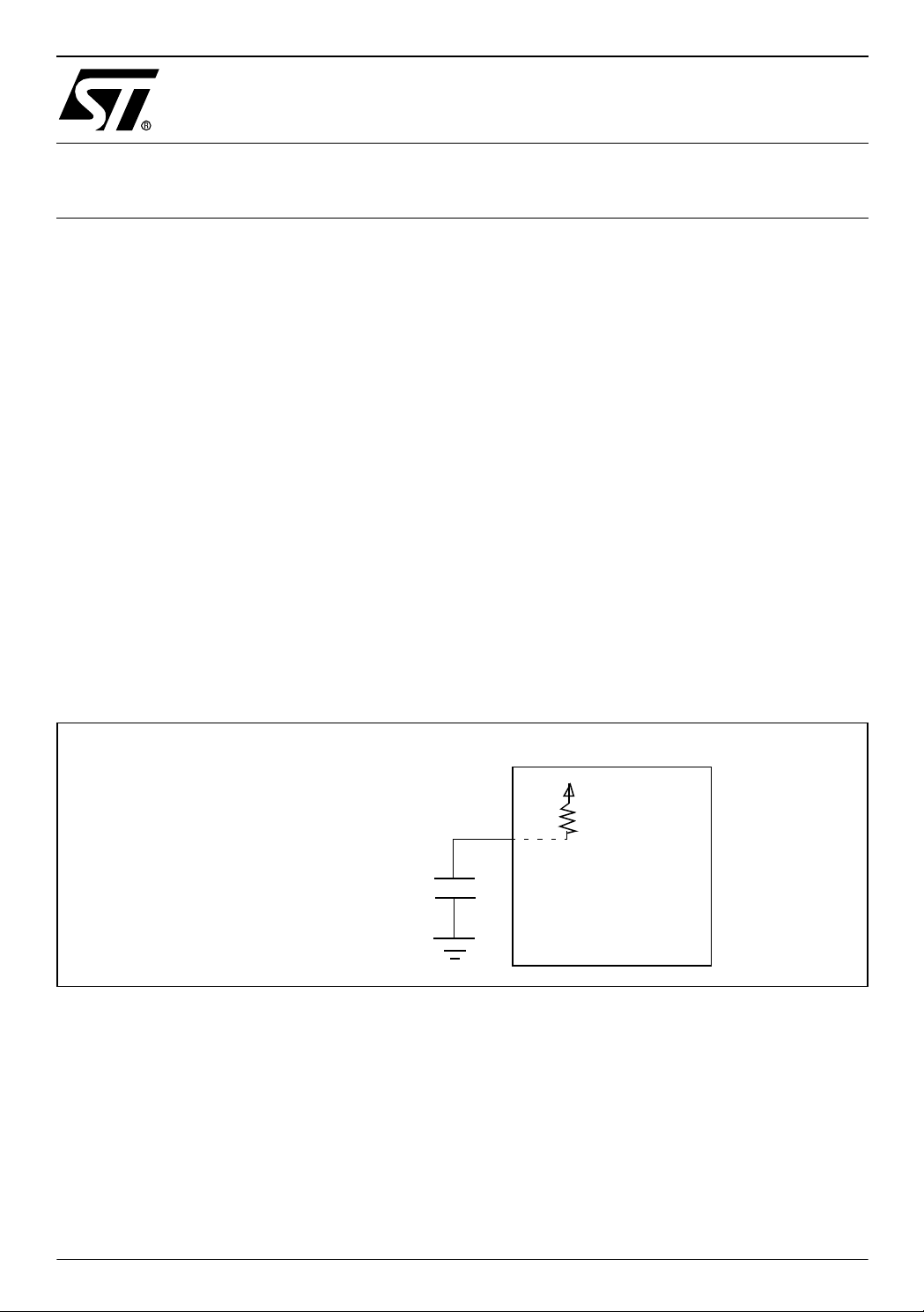
1.1 HARDWARE SOLUTION
Figure 1 shows the Hardware setup used to measure the consumption (I
supply voltages.
Figure 1. Hardware Setup
V
DD
R
EI0
PA0
C
EXT
1.2 POWER CONSUMPTION
The power consumption depends mainly on the time period between each wakeup from HALT
(external interrupt interval). The wakeup time period i s controlled by the RC time constant. The
value of the C
voltage and with temperature.
is fixed but the internal pull-up value varies with the MCU power supply
ext
PU
) at different power
DD
AN1605/0403 1/7
1
Page 2
The typical values of the Rpu at different power supply voltages is given in Table 1.
Table 1. Rpu values for different power supply conditions
Setup No. Conditions Rpu (Minimum) Rpu (Typical) Rpu (Maximum)
1V
2V
= 5.0 V 50 kΩ 120 kΩ 250 kΩ
DD
= 3.0 V - 160 kΩ -
DD
The consumption is measured for two different values of C
Table 2. Consumption for C
Average I
Setup No. V
(Volts)
DD
Consumption in
= 1 µF
ext
(mA )
DD
Run mode
Average I
DD
(µA)
Consum pt i on i n
Power saving
mode
, given in Table 2 and Table 3.
ext
Ext Interrupt
Interval (ms)
1 2.4 1.44 15.6 154.0
2 2.6 1.73 20.6 131.2
3 2.8 2.0 26.6 114.0
4 3.0 2.28 35.2 101.2
5 3.2 2.59 41.8 90.8
6 3.4 2.95 48.6 80.8
7 3.6 3.34 56.6 72.4
8 3.8 3.55 66.2 67.2
9 4.0 3.73 75.3 62.6
10 4.2 3.93 83.4 59.2
11 4.4 4.12 95.4 55.2
12 4.6 4.31 105.2 53.0
13 4.8 4.54 117.4 50.6
14 5.0 4.75 129.4 48.0
I
(µA)
DD
Consumption
when MCU is in
HALT
0.1
2/7
2
Page 3
Table 3. Consumption for C
Setup No. VDD (Volts)
= 0.47 µF
ext
Average I
DD
(mA)
Consumption
in Run mode
Average IDD (µA)
Consumption in
Power saving
mode
Ext Interrupt
Interval (ms)
1 2.4 1.45 19.6 69.8
2 2.6 1.74 25.1 60.0
3 2.8 2.01 32.1 52.2
4 3.0 2.29 39.0 46.6
5 3.2 2.60 46.2 42.1
6 3.4 2.95 54.2 38.0
7 3.6 3.34 62.5 35.2
8 3.8 3.54 71.7 32.8
9 4.0 3.75 81.2 30.8
10 4.2 3.91 91.8 29.2
11 4.4 4.12 101.9 27.7
12 4.6 4.31 112.6 26.5
13 4.8 4.51 124.0 25.4
14 5.0 4.73 135.4 24.3
The parameters on which the consumption depends are as follows:
I
(µA)
DD
Consumption
when MCU is in
HALT
0.1
■ The MCU inserts a delay of 256 C PU cycles to stabilize the internal RC, d uring this time it
consumes some current.
For example at 3.6V, the details of the duration of different modes are as follows:
– MCU in Halt mode: 72.00 ms
– MCU in Run mode (delay period + capacitor discharge time) : 211.2 µs
3/7
Page 4

Figure 2. Overview of the Consumption Parameters
mA
I
DD
3.5
Halt mode
0.0002
Run mode
72ms
TEMPO
Run modeHalt mode T
211µs
t
The exact calculation of the delay period is given as follows:
When the PLLx4x8 is selected, it delivers the clock after 60 cycles of the clock source (for a 1
MHz clock source, the delay due to the PLL is 60µs).
The total delay at oscillator start up with PLLx4x8 is given by the formula:
Ttempo = [(60*Tclock_source) + (256*Tcpu_clock)]
where,
Tclock_source represents the time period for one clock cycle of the clock source, and
Tcpu_clock represents the time for one cpu clock cycle.
■ To discharge the capacitor, a software delay of 294 cycles has to be inserted before putting
the MCU in Halt again, so that the capacitor is fully discharged before recharging it. This i s
the optimum delay at which minimum consumption is achieved.
■ For minimum consumption in Halt mode: all the port pins should be configured as push pull
output at low level (normally the consumption in this configuration is approx. 0.1 ~ 0.2 uA),
but the pin to which the external interrupt is connected (PA0), has to be configured as pull up
interrupt. Hence, while the MCU is in Halt mode with this configuration, it consumes mor e
than 0.2 µA.
■ The MCU cannot be kept in Halt for longer than the time it takes the capacitor to charge up
to Vdd level. This is because as soon as the capacitor charges to approximately 0.7Vdd, the
MCU detects it as external interrupt (the interrupt sensitivity is configured for rising edge)
and comes out of Halt mode.
4/7
Page 5

■ The charging time is mainly controlled through the capacitor value. But if the capacitor value
is increased beyond 1uF, although the interval between external interrupts (in ms) is
increased, the capacitor itself c onsumes more current while charging. Hence, the average
consumption is high in this case. A summary of the consumption and the external interrupt
interval for C
= 2.2uF and 4.7uF i s shown in Table 4 . It can be seen from this table that
ext
even though the external interrupt interval is longer than in Tables 2 & 3, the consumption is
higher.
Table 4. Power Consumption and Ext. Interrupt Interval for C
C= 2.2µF C= 4.7µF
Setup
No.
1 3.0 35.6 171.6 48.9 200.0
2 4.0 86.4 107.6 114.5 124.2
3 5.0 146.6 83.6 189.6 97.2
V
DD
(Volts)
Aver age I
Consumption in
power saving
mode
DD
(µA)
Ext Interrupt
Interval (ms)
Average I
Consumption in
= 2.2 µF and C
ext
(µA)
DD
Power saving
mode
= 4.7 µF
ext
Ext Interrupt
Interval. (ms)
If a different hardware setup is used, where an external series R (to generate the external interrupt through an external RC combination) is connected, the capacitor charging time decreases drastica lly. Fo r exam ple, whe n a serie s R of 49 0K is adde d, the chargin g time de creases to 6.7µs. Hence, the period the MCU stays in Halt mode is very small, causing more
consumption.
As a conclusion, the best result (minimum consumption) is achieved with a 1µF capacitor
value and using an internal pullup. This is illustrated in Figure 3.
Figure 3 shows th e aver age I
consumption in Halt mode and Run mode respe ctively with
DD
the two different capacitor values (Cext = 1.0 uF and 0.47uF) used for the active RC.
5/7
Page 6

Figure 3. Average IDD Consumption Run and Halt Mode
A
5
4.5
4
3.5
3
2.5
2
1.5
1
0.5
Average Consumption IDD (m
0
2.4 3 3.6 4.2 4.8 5
Run mode (Cext= 1. 0uF)
Run mode (Cext= 0. 47uF)
Vdd (Volts)
0.16
0.14
0.12
0.1
0.08
0.06
0.04
0.02
Average Consumpt i on IDD (uA)
0
Halt m ode (Cext=1.0uF)
Halt m ode (Cext=0.47 uF )
2.4 3 3.6 4. 2 4.8 5
Vdd ( Volt s)
1.3 SOFTWARE SOLUTION
The software is written in assembly.
First the PA0 port (through which the external interrupt is taken to the MCU) is configured as
pull-up interrupt.
The sensitivity of the interrupt is configured as rising edge.
Then the capacitor is charged through software and immediately the MCU is put into HALT.
As soon as the capacitor charges to nearly 0.7Vdd, the MCU detects it as an external interrupt
and comes out of Halt mode.
The capacitor is discharged through software. And a small software delay of 294 cycles is then
provided to let the capacitor discharge fully before it recharges and wakes up the MC U from
Halt mode with another external interrupt.
The MCU is again put into Halt and the same process is repeated.
All the source files in assembly code is given in the zip file with this application note.
The source files are for guidance only. STMicroelectronics shall not be held liable for any di-
rect, indirect or consequential damages with respect to any claims arising from use of this s oftware.
6/7
Page 7

THE PRESENT NOTE WHICH IS FOR GUIDANCE ONLY AIMS AT PROVIDING CUSTOMERS WITH INFORMATION
REGARDING THE IR PRO DUCT S IN OR DER FO R THEM TO SAV E TIME . AS A RES ULT, STMIC ROEL ECTR ONI CS
SHALL NOT BE HELD LIABLE FOR ANY DIRECT, INDIRECT OR CONSEQUENTIAL DAMAGES WITH RESPECT TO
ANY CL AIM S AR IS IN G FR OM T HE CO N TENT OF S UC H A NO TE A ND /O R T HE U SE M AD E BY C US TO ME RS O F
THE INFORMATION CONTAINED HEREIN IN CONNECTION WITH THEIR PRODUCTS.”
Information furnished is believed to be accurate and reliable. However, STMicroelectronics assumes no responsibility for the consequences
of use of such information nor for any infringement of patents or other rights of third parties which may result from its use. No license is granted
by implic ation or otherwise under any patent or patent ri ghts of STM i croelectr oni cs. Spec i fications mentioned i n this publication are subje ct
to change without notice. This publication supersedes and replaces all information previously supplied. STMicroelectronics products are not
authorized for use as cri tical comp onents in life support dev i ces or systems wi thout the express written approv al of STMicroel ectronics.
The ST logo is a registered trademark of STMicroelectronics
2003 STMicroelectronics - All Rights Reserved.
STMicroelectronics Group of Compan i es
http://www.s t. com
Purchase of I
2
C Components by STMicroelectronics conveys a license under the Philips I2C Patent. Rights to use the se components in an
2
I
C system i s granted pro vi ded that the sy stem conforms to the I2C Standard Specification as defined by Philips.
Australi a - B razil - Canada - China - Finl and - France - Germany - Hong Kong - Ind ia - Israel - Italy - Japan
Malaysi a - M al ta - Morocco - Singapore - Spain - Sw eden - Switz erland - United Kingdom - U.S.A.
7/7
 Loading...