

Page 1

AN1602
APPLICATION NOTE
16-BIT TI MIN G OP ER ATIONS US ING ST 72 62 O R S T 7263 B
MCUs
Microcontroller Division Applications
INTRODUCTION
This Application Note describes how to us e the ST7262 or ST 7263B for 1 6-bit timin g operations. The intention of this document is to show how to perform pulse measurement and PWM
generation using the different timers available on each microcontroller type.
1 16-BIT TIMING MEASUREMEN TS
1.1 USING ST7262
The aim of this section is to describe how to use the ST7262 8-bit timer to perform pulse and
frequency measurements with 16-bit accuracy.
1.1.1 16-Bit Capture
1.1.1.1 Principle
The ST7262 architecture allows you to cascade the 8-bit Auto Reload Timer (ART) with the 8bit Time Base Unit (TBU) to obtain a 16-bit counter (The carry bit of the ART acts as the clock
for the TBU). Using t his configuration, the ARTCAR register represents the Least S ignificant
Byte and the TBUCV register represents the Most Significant Byte (see Figure 1).
Figure 1. TBU+ART 16-Bit Counter Value
TBU (MSB)
16 Bit Counter Value
On each valid input capture, the 16-bit counter value is obtained by:
– The ARTCAR register which is automatically latched.
– The TBUCV register which is saved by software in the Input Capture Interrupt routine.
This method ensures a “real-time” capture of the low bits, while the software delay needed to
save the TBUCV can be compensated.
ART (LSB)
AN1602/0503 1/21
1
Page 2
16-BIT TIMING OPERAT IONS USING ST7262 OR ST7263B MCUs
1.1.1.2 Delay Compensation method
The software delay introduced by the interrupt routine should be taken into account otherwise
the measurement value can be corrupted. This happens if the ART counter rolls over from FFh
to 00h while soft ware is s toring the TB UCV v alue afte r a v alid input cap ture interrup t. In this
case, the TB UCV is in cremen ted and a wr ong value oc curs in the 8th bit of th e 16-b it input
capture value.
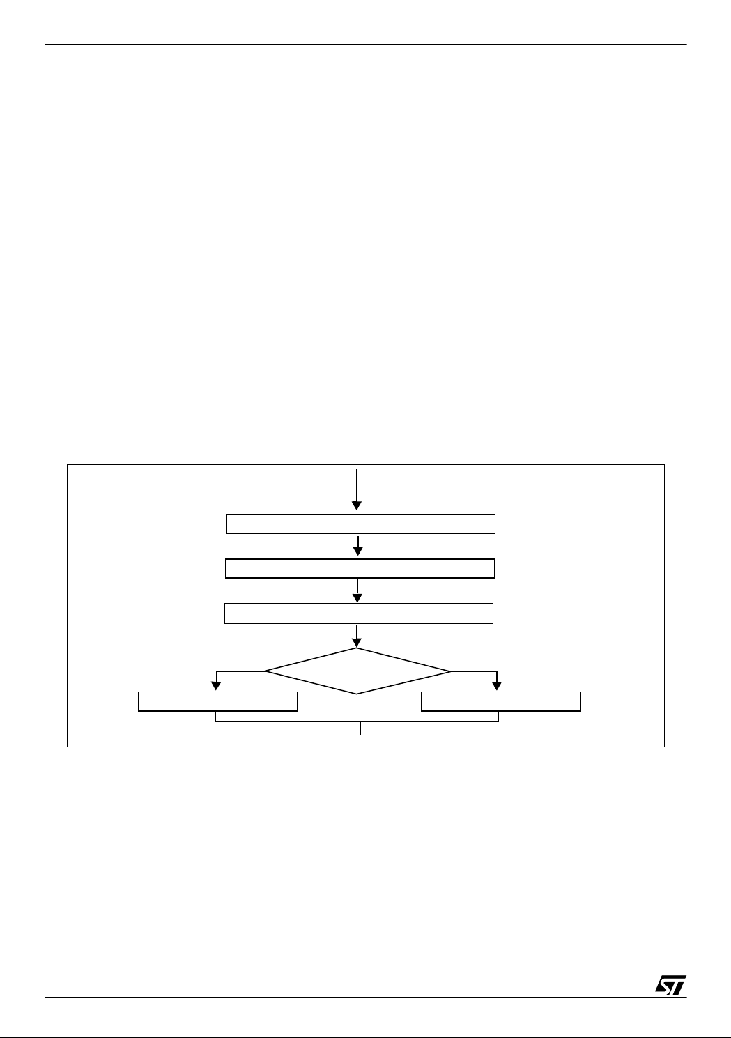
The delay compensation method is described in the following flowchart (Figure 2).
The first step consists of transferring both TBU and ART values into temporary variables
(TmpTBU1, TmpAR T, Tmp TBU 2) to be used later on. Then in t he s econd s tep we com pare
TmpART and ICxR. There are two cases to be considered:
– TmpART >= ICRx: This means that the ART counter value was incremented by a few cycles
but has not yet reached the maximum value (FFh). In this case we use TmpT BU1.
– TmpART < ICRx:This means that the ART counter was incremented beyond the maximum
value and has been reset. This means we should decrement TmpTBU2 once to get the right
value of TBUCV.
Figure 2. TBU Delay Compensation flowchar t
Interrupt From ICAP1 or ICAP2
Read & Store the TBUCV in TmpTBU1
Read & Store the ARTCAR inTmpART
Read & Store the TBUCV in TmpTBU2
Yes
TmpART >= ICxR
TBUok= TmpTBU1 TBUok= TmpT BU2 - 1
No
1.1.1.3 Example of an interrupt capture routine
The input capture inte rrupt rou tine given below ca n be us ed to get t he prec ise va lue of t he
input capture interrupt instant on ICAP1 pin. It can be used to detect a ri sing or falling edge depending on the configured edge in ARTICSR.
.Inp_Cap_Routine
;----------------------------------------;
Ld A , TBUCV ;Load the TBU counter value
2/21
2
Page 3
16-BIT TIMING OPERAT IONS USING ST7262 OR ST7263B MCUs
Ld TmpTBU1 , A ;into TmpTBU1
Ld A , ARTCAR ; Load the ART counter Value
Ld TmpART1 , A ;into TmpART1
Ld A , TBUCV ; Load the TBU counter value into
Ld TmpTBU2 , A ;TmpTBU2
;----------------------------------------;
Ld A , TmpART1 ; Compare ART & ICR
Cp A , ARTICR2 ; If ART > ICR then Case 2
jrpl Case2 ;
Ld A , TmpTBU2 ; Case 1 : TBU = TBU2 - 1
Dec A ;
jra Next2 ;
.Case2 Ld A , TmpTBU1 ; Case TBU = TBU1
.Next2 Ld PulseEndHR , A ;load TBUCV into PulseEndHR
Ld A , ARTICR2 ;Load The ART Inp Capt 2 register
Ld PulseEndLR , A ;Value into PulseEndLR
Ld A , ARTICCSR ;Clear The input capture interrupt
Iret ;Exit From Interrupt
1.1.2 Pulse Length measurement
1.1.2.1 Measurement Principles
As first example in this application note, we will try to measure the pulse length of an external
signal applied to the input capture pins.
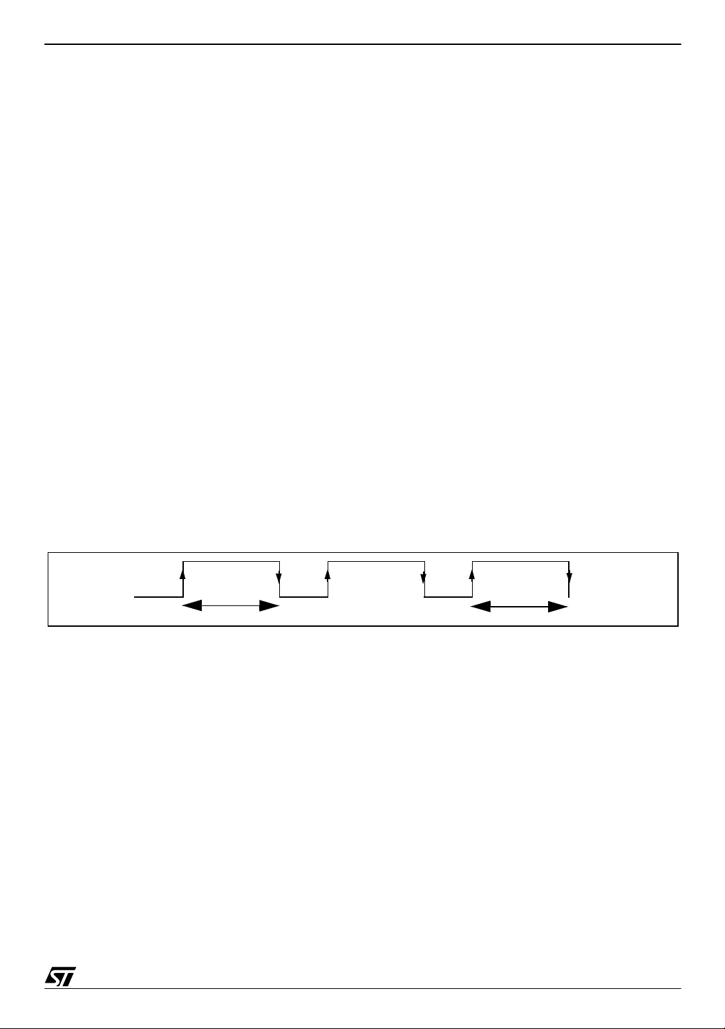
Figure 3. Pulse Length Measurement
Pulse Length
To perform this operation, two input captures are used together and they are configured as fol lows:
– Input capture1 pin (ARTIC1) configured to detect rising edges
– The input capture2 pin (ARTIC2) configured to detect falling edges
The ARTIC1 & ARTIC2 are connected together (Figure 4).
Two 16-b its vari ables ar e used t o hold th e 16-bi ts time r values on ea ch vali d input capture
edge (PulseStart for the rising edge and PulseEnd for the edge).The pulse length value can be
deduced later using a 16-bits substruction between PulseStart and PulseEnd
3/21
Page 4
16-BIT TIMING OPERAT IONS USING ST7262 OR ST7263B MCUs
Figure 4. Input Capture Configuration
ST7262
ARTIC1
External Signal
ARTIC2
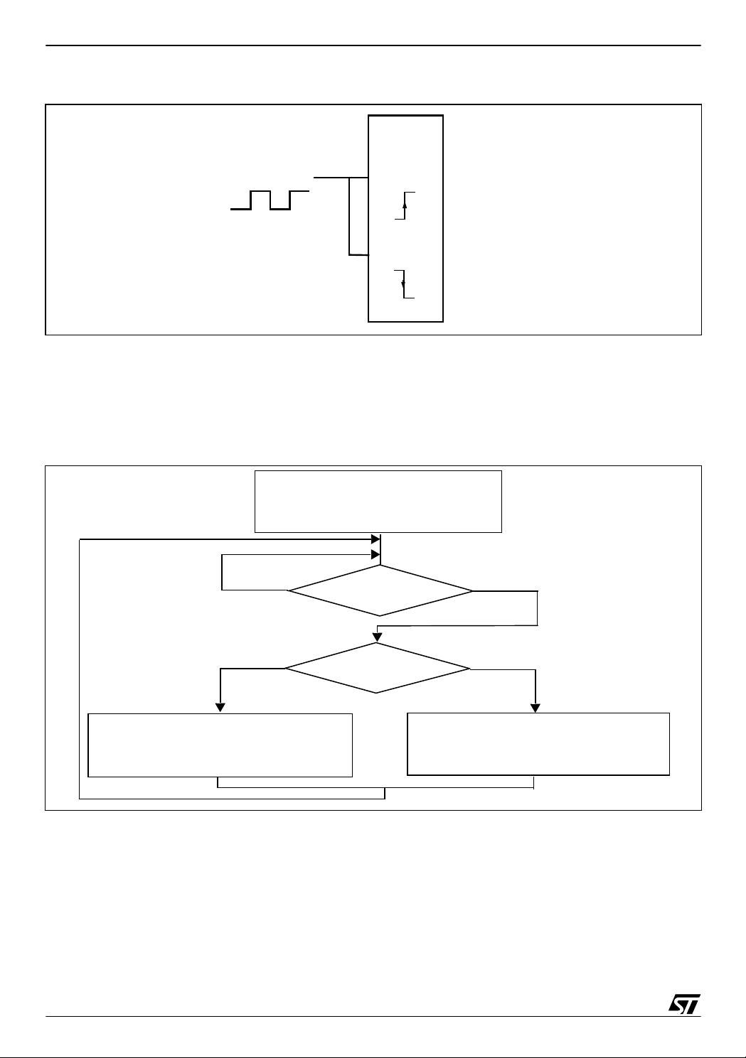
Figure 5 shows the steps that have to be followed to successfully measure the length of a
pulse in 16-bit accuracy.
Figure 5. Input Capture Sequence
- Configure Time clock frequency
- Select edge sensitivity on ICAP pins
- Cascade PWMART & TBU
No
Input capture interrupt
ICAP1
- Store the TBU counter Value
(Compensated value) in PulseStartHR
- Store the ICRx Value in PulseStartLR
ICAP1 Or ICAP2
- Store the TBU counter Value
(Compensated value) in PulseEndHR
- Store the ICRx Value in PulseEndLR
YES
ICAP2
1.1.2.2 Example of input capture interrupt rout ine
.Inp_Cap_Routine ;
Btjt ARTICCSR,#0,Flag1 ; Test If is ICAP(1 Or 2)
.Flag2 Ld A , ARTICR2 ; Latch the Input Cap Reg into
Ld IcapReg2 , A; IcapReg2
Ld A , ARTICCSR ; Clear Interrupt
4/21
1
Page 5

16-BIT TIMING OPERAT IONS USING ST7262 OR ST7263B MCUs
Ld A , TBUCV ; Load the TBU counter value
Ld TmpTBU1 , A; into TmpTBU1
Ld A , ARTCAR ; Load the ART counter Value
Ld TmpART1 , A ; into TmpART1
Ld A , TBUCV ; Load the TBU counter value into
Ld TmpTBU2 , A; TmpTBU2
Ld A , TmpART1 ; Compare ART & ICR
Cp A , IcapReg2 ; If ART > ICR then Case 2
jrpl Case2 ;
Ld A ,TmpTBU2; Case 1 : TBU = TBU2 - 1
Dec A ;
jra Next2 ;
.Case2 Ld A , TmpTBU1 ; Case TBU = TBU1
.Next2 Ld PulseEndHR , A; load TBUCV into PulseEndHR
Ld A , IcapReg2 ; Load The ART Inp Capt 2 register
Ld PulseEndLR , A; Value into PulseEndLR
Iret ; Exit from Interrupt
.Flag1 Ld A , ARTICR1 ; Latch the Input Cap Reg into
Ld IcapReg1 , A; IcapReg1
Ld A , ARTICCSR ; Clear Interrupt
Ld A , TBUCV ; Load the TBU counter value
Ld TmpTBU1 , A; into TmpTBU1
Ld A , ARTCAR ; Load the ART counter Value
Ld TmpART1 , A ; into TmpART1
Ld A , TBUCV ; Load the TBU counter value into
Ld TmpTBU2 , A; TmpTBU2
Ld A , TmpART1 ; Compare ART & ICR
Cp A , IcapReg1 ;
jrpl Case1 ;
Ld A , TmpTBU2; Case : TBU = TBU2 - 1
Dec A ;
jra Next1 ;
.Case1 Ld A , TmpTBU1 ; Case TBU = TBU1
.Next1 Ld PulseStartHR , A; load TBUCV into PulseEndHR
Ld A , IcapReg1 ; Load The ART Inp Capt 2 register
Ld PulseStartLR , A; Value into PulseEndLR
Iret ; Exit from Interrupt
1.1.3 Frequency Measurement
1.1.3.1 Measurement Principles
Frequency measurement is a little bit different from pulse length measurement. To get the frequency, we measure the full signal period which can be defined by the time interval between
two consecutive rising edges (Figure 6)
5/21
Page 6
16-BIT TIMING OPERAT IONS USING ST7262 OR ST7263B MCUs
Figure 6. Frequency Measurement
Frequency= 1 / Period
In this example w e will al so use two 16 -bit variables to h old the 1 6-bit timer v alue eac h tim e
an input c aptur e oc c urs ( Sta r tPer iod: for the f irst ri sing e dge and E nd Peri od f or the s e cond
falling edge). In addition to thes e two variables, we will nee d an extra variable (FirstEdge)
which is used to indicate the first rising edge or the second edge.
– FisrtEdge =0: First Rising edge (PeriodStart)
– FisrtEdge =1: Second Rising edge (PeriodEnd)
In this case we will need only one input capture pin (ARTIC1) c onfigured to detect only rising
edge.
The capture steps are shown in Figure 7. After selecting the timer frequency and the input
capture edge we wait for an input capture interrupt. Depending on the FirstEdge value the
input capture parameters (ICxR and the TBU) are transferred into PeriodStart or PeriodEnd.
Figure 7. Input Capture Sequence
- Configure Time clock frequency
- Select sensitive edge on ICAP pins
- Cascade PWMART & TBU, FirstEdge = 0
No
0
- Store the TBU (compensated value)
in PeriodStartHR
- Store the ICxR in PeriodStartLR
input capture
First Edge =?
- Store the TBU (compensated value)
in PeriodEndHR
- Store the ICxR Value in PeriodEndLR
YES
1
6/21
Page 7

16-BIT TIMING OPERAT IONS USING ST7262 OR ST7263B MCUs
1.1.3.2 Example of input capture interrupt rout ine
.Inp_Cap_Routine ;
Ld A , ARTICR1 ;
Ld CurrentICAP , A ;
;------------------------------------------;
Ld A, ARTICCSR ;
;------------------------------------------;
Ld A , TBUCV ;Load the TBU counter value
Ld TmpTBU1 , A ;into TmpTBU1
Ld A , ARTCAR ;Load the ART counter Value
Ld TmpART1 , A ;into TmpART1
Ld A , TBUCV ;Load the TBU counter value into
Ld TmpTBU2 , A ;
;------------------------------------------;
Btjf FirstEdge,#0,FirstRisingEdge ;TmpTBU2
;------------------------------------------;
;.SecondRisingEdge ;
Ld A , TmpART1 ;Compare ART & ICR
Cp A , CurrentICAP ;If ART > ICR then Case 2
jrpl Case2 ;
Ld A , TmpTBU2 ;Case 1 : TBU = TBU2 - 1
Dec A ;
jra Next2 ;
.Case2 Ld A , TmpTBU1 ;Case TBU = TBU1
.Next2 Ld PeriodEndHR , A ;load TBUCV into PeriodEndHR
Ld A , CurrentICAP ;Load The ART Inp Capt 1 register
Ld PeriodEndLR , A ;Value into PeriodEndLR
Clr FirstEdge ;
Iret ;
.FirstRisingEdge ;
Ld A , TmpART1 ;Compare ART & ICR
Cp A , CurrentICAP ;
jrpl Case1 ;
Ld A , TmpTBU2 ;Case : TBU = TBU2 - 1
Dec A ;
jra Next1 ;
.Case1 Ld A , TmpTBU1 ; Case TBU = TBU1
.Next1 Ld PeriodStartHR , A ;load TBUCV into PulseEndHR
Ld A , CurrentICAP ;Load The ART Inp Capt 1 register
Ld PeriodStartLR , A ;Value into PulseEndLR
Inc FirstEdge ;
Iret ;
7/21
Page 8

16-BIT TIMING OPERAT IONS USING ST7262 OR ST7263B MCUs
1.2 USING ST7263B
This section describe how to use the ST7263B 16-bit timer to perform 16-bit timing
operations such as period and pulse length measurement.
1.2.1 The Input Capture operation
In the case of the ST 7263B both ICA P1 and ICAP2 are as sociated with 16 -bit registers
(TIC1HR, TIC1LR, TIC2HR and TIC2LR). These registers are used to hold the corresponding
16-bit timer value at each valid input capture (see Figure 8).
Figure 8. Input Capture Registers
TIC1LR (LSB)
TIC2LR (LSB)
ARTIC1(16-bit Register)TIC1HR (MSB)
ARTIC2(16-bit Register)TIC2HR (MSB)
1.2.2 Pulse Length measurement
1.2.2.1 Measurement principles
To measu re p ulse len gth , two input captu res a re us ed tog ether. The input captu re1 pin
(ICAP1) is configured to detect rising edge and the input capture2 pin (ICAP2) is configured to
detect falling edge. The ICAP1 & ICAP2 pins are connected together and on each input capture: rising edge or falling edge two 16-bit variables are used to hold the 16-bit timer value.
Figure 9. Input Capture sequence
- Configure Time clock frequency
- Select edge sensitivity edge on ICAP
No
ICAP1
- Store the TIC1HR in PulseStartHR
- Store the TIC1LR in PulseStartLR
input capture
ICAP1 or ICAP2
YES
ICAP2
- Store the TIC2HR in PulseEndHR
- Store the TIC2LR in PulseEndLR
Whenever a valid rising edge is captured, the timer counter value is automatically stored in the
TIC1HR & TIC1LR registers. These two registers act together as one 16-bit register that holds
the counter value to be transferred into PulseStart (PulseStartHR & PulseStartLR).Whenever
a valid falling edge is captured, the timer counter value is automatically stored in the TIC2HR
8/21
Page 9

16-BIT TIMING OPERAT IONS USING ST7262 OR ST7263B MCUs
& TIC2LR registers. These two register s act together as one 16-bit register that holds the
counter value to be stored in PulseEnd (PulseEndHR & PulseEndLR).
1.2.2.2 Example of input capture interrupt rout ine
.Input_Capt_Rt
Btjt TSR , #7 , Flag1 ; Test Rising or falling edge ?
.Flag2 ; Falling Edge
Ld A , TSR ; Clear Interrupt Flag
Ld A , TIC2HR ; Load TIC2R ( HR & LR ) into
Ld PulseEndHR , A; PulseEnd ( HR & LR )
Ld A , TIC2LR ;
Ld PulseEndLR , A;
Iret ;
.Flag1 ; Rising Edge
Ld A , TSR ;Load TIC1R ( HR & LR ) into
Ld A , TIC1HR ; PulseStart ( HR & LR )
Ld PulseStartHR , A;
Ld A , TIC1LR ;
Ld PulseStartLR , A;
Iret ;
1.2.3 Frequency Measurement
1.2.3.1 Measurement principles
To measure frequency we will us e the same technique we us ed for the ST7262 (see Sec tion
1.1.3). We need only one input capture pin configur ed to detect rising edg es and two 16-bit
variables to hold the 16-bit timer value at each input capture occurrence (StartPeriod) and
(EndPeriod). We w ill n eed a lso Fi rstEdge w hich indicate s the first r ising edg e or the s econd
edge.
9/21
Page 10

16-BIT TIMING OPERAT IONS USING ST7262 OR ST7263B MCUs
Figure 10. Input Capture Sequence
- Configure Time clock frequency
- Select sensitive edge on ICAP pin
- FirstEdge = 0
No
0
- Store the IC1HR Value in PeriodStartHR
- Store the IC1LR Value in PeriodStartLR
- Increment FirstEdge
Input capture interrupt
First Edge =?
- Store the ICP2HR Value in PeriodEndHR
- Store the ICP2LR Value in PeriodEndLR
-Decrement FirstEdge
1.2.3.2 Example of input capture interrupt rout ine
.Input_Capt_Rt
Ld A , TIC1HR ; Lock The TICR
Btjf FirstEdge ,#0, FirstRisingEdge ; Test First Or Second Edge
.SecondRisingEdge ;
Ld PeriodEndHR , A; Load PriodEnd Values
Ld A , TIC1LR ;
Ld PeriodEndLR , A;
Ld A , TSR ;Clear ICAP interrupt Flag
Ld A , TIC1LR ;
Clr FirstEdge ;
Iret ;
.FirstRisingEdge ;
Ld PeriodStartHR , A ; Load PriodStart Values
Ld A , TIC1LR ;
Ld PeriodStartLR , A ;
Ld A , TSR ;Clear ICAP interrupt Flag
Ld A , TIC1LR ;
Inc FirstEdge ;
Iret ;
YES
1
10/21
Page 11

16-BIT TIMING OPERAT IONS USING ST7262 OR ST7263B MCUs
1.3 PERIOD MEASUREMENT CAPABILITY
This section describes a comparison based on period measurement capability (rising edge to
rising edge measurement) between the ST7262 16-bit timer (ART + TBU) and ST7263B 16-bit
timer. All comparisons and measurement range values are calculated using the software provided with this application note and at f
= 8 MHz.
CPU
1.3.1 Using the ST7262 ART & TBU in cascading mode
Analyzing the ST7262 period measurement capability in the cascading mode can be done by
focusing o n tw o imp ortan t p oints : t he m axim um period and th e m inimu m p erio d t hat c an be
measured using this mode.
1.3.1.1 Maximum period
In cascading mode, the timer acts as a 16-bit free running counter. At f
imum period can reach t
max
t
= FFFFh * Timer
max
= 65535 Timer
clk
clk
= 8 MHz, the max-
CPU
Table 2 shows the time measurement range covered by the ST7262 ART & TBU timer.
Table 1. Time M easurement Range using ART & TBU
Prescaler Timer Frequency Maximum Period Resolution
1
2
4
8
16
32
64
8 MHz 8,192 ms 0.125 µs
4 MHz 16,384 ms 0.250 µs
2 MHz 32,767 ms 0.500 µs
1 MHz 65,535 ms 1 µs
500 kHz 131,07 ms 2 µs
250 kHz 262,14ms 4 µs
125 kHz 524,28 ms 8 µs
128
62.5 kHz 1048,56 ms 16 µs
1.3.1.2 Minimum period
The minimum period that can be meas ured using the ST7262 16-bit timer depends on several
parameters such as the software delay introduced by interrupt routine execution time and the
hardware delay required to enter and exit the interrupt subroutine.
11/21
Page 12

16-BIT TIMING OPERAT IONS USING ST7262 OR ST7263B MCUs
Figure 1 1 sho ws the nor m al be havio ur of t he in put ca ptur e r out ine: e ach r isi ng e dg e is d etected and the inp ut captur e interr upt routine is ex ecuted aft er the T0 del ay. In t his c ase the
period measurement operation can be easily done.
Figure 11. Case 1: Interrupt routine execution sh orter than period to be measured
T
T
1
T
0
T: Period of the external signal to be measured
T
: Interrupt routine execution time
1
T
: Delay needed to activate the interrupt routine
0
T
T
1
T
0
T
0
The minimum period that can measured depends strongl y on the number of rising edges
during the interrupt routine execution.
A single rising ed ge d uring the ex ecution of the in terrupt r outine does n ot c orrupt the meas urement value and the period measure ment o peration ca n be achieved s uccessfully (F igure
12).
Figure 12. Case 2: Interrupt routine execution lo ng er than period to be measured
T
T
T
1
T
0
T: Period of the external signal to be measured
T
: Interrupt routine execution time
1
T
: Delay needed to activate the interrupt routine
0
T
: Delay needed to exit from interrupt routine
2
T
1
T
2
However, any addi tional r ising edg e leads to a corr upted measur ement. As s hown in Figur e
12, the second rising edge is ignored, in fact before executing the input capture interrupt triggered by the second rising edge, a third one occurs and overwrites the previous ICxR value.
For this reason the period measurement operation result is corrupted
(result = 2 * T).
12/21
Page 13

16-BIT TIMING OPERAT IONS USING ST7262 OR ST7263B MCUs
So the minimum period (the maximum frequency) that can be measured using the ST7262 16bits cascaded timer can be calculated using the following formula.
Figure 13. Minimum measurable period (max. frequency)
123123
T
T
1
T
0
T0: Time needed to activate the interrupt routine (10 t
ternal clock rising edge (about 2 t
: Time needed to execute the interrupt routine. Using the example software supplied in this
T
1
application note, the input capture interrupt routine needs about 62 t
: The time needed to exit from the interrupt routine (9 t
T
2
: This represents the period of time from the start of the interrupt routine until the ICxR reg-
T
3
ister is read (about 3 t
in the example software).
CPU
T
2T > T
CPU
T
T
0
0+T1+T0+T2+T3
).
T
3
2
T
1
), and the time need to wait for the in-
CPU
.
CPU
).
CPU
Using the above values based on the software example:
= 10, T1 = 62 t
T
0
CPU
, T2 = 9 t
CPU
, T3 = 3 t
CPU
2 T > T
2 T > (12 + 62 + 12 + 9 + 3) * t
0+T1+T0+T2+T3
CPU
> 98 * 0.125 µs
> 12.25
So we can calculate the minimum period Tmin = 6.125 µs.
1.3.2 Using the ST7263B 16-bit timer
1.3.2.1 Maximum Period
Using the ST7263B 16-bit timer, the ma ximum meas urable period t
can be expressed as
max
follows:
= FFFFh * Timer
t
max
= 65535 Timer
clk
clk
So the maximum period that can meas ured using the S T7263B 16- bit timer and the ST7262
cascaded timer is the same, however the minimum period is different.
13/21
Page 14

16-BIT TIMING OPERAT IONS USING ST7262 OR ST7263B MCUs
Table 2. Time measurement range using ST7263B
Prescalers Timer Frequency Maxi Period Resolution = 1 t
2 4 MHz 16,384 ms 0.250 µs
4
8
2 MHz 32,767 ms 0.500 µs
1 MHz 65,535 ms 1 µs
CLK
1.3.2.2 Minimum Period
In the case of ST7263B, on each valid input capture, the 16-bit counter value is latched automatically into the 16-bit input capture registers ( TICxHR & TICxLR) without any additional software routin e. So co mpared to th e ST7 262 , th e ST 7 26 3B need s les s tim e to st ore the i np ut
capture parameters into temporary variables.
Using the same method as for the ST7262 (see Figure 13):
2T > T
0+T1+T0+T2+T3
And with the following parameters:
T
0
= 12 t
CPU
(10 t
for the interrupt activation and 2 t
CPU
the maximum time needed to syn-
CPU
chronise the interrupt flag with the internal CPU frequency).
T
1
= 26 t
CPU
=9 t
T
2
CPU
T3 = 23 t
(from the start of the interrupt routine until the interrupt flag is cleared).
CPU
Using the above values based on the software example:
= 12, T1 = 26 t
T
0
CPU
, T2 = 9 t
2 T > T
, T3 = 23 t
CPU
0+T1+T0+T2+T3
2 T > (12 + 26 + 12 + 9 + 23) * t
CPU
CPU
> 82 * 0.125 µs
> 10.25 µs
So we can calculate the minimum period Tmin = 5.125 µs.
1.3.2.3 Period Measurement Comparison Chart
The follo win g tabl e can be u sed to sel e ct t he b es t presc aler v alue f or a preci se tim e or fre quency measurement with the appropriate resolution.
14/21
Page 15

16-BIT TIMING OPERAT IONS USING ST7262 OR ST7263B MCUs
Table 3. Period Measurement Capability Com parison Chart
Max.
ms
16-Bit Timer
ART & TBU
(ST7262)
Re-
solution
16 µs 0.953 Hz
Freq.
8-Bit Timer
ART
(ST7262)
Max.
Measure
Pre-
scaler
1 31,875 µs 0.125 µs
2 63,750 µs 0.25 µs
4 127,5 µs 0.5 µ s
8 255 µs 1 µs
16 510 µs 2 µs
32 1.02 ms 4 µs 998 Hz 262, 14 ms 4 µs 3,815 Hz
64 2.04 ms 8 µs 499 Hz 524, 28 ms 8 µs 1.907 Hz
128 4.08 ms 16 µs 249,5 Hz
ment
Period
Re-
solution
Freq.
31,372
kHz
15,686
kHz
7,843
kHz
3,921
kHz
1,996
kHz
Measure
ment
Period
8,192 ms 0.125 µs 122,1 Hz
16,384 ms 0.250 µs 61.05 Hz 16 ,384 ms 0.25 µs 61.05 Hz
32,767 ms 0.5 µs 30.52 Hz 32 ,767 ms 0.5 µs 30.52 Hz
65,535 ms 1 µs 15.26 Hz 65,535 ms 1 µs 15.26 Hz
131,07 ms 2 µs 7.63 Hz
1048,56
Max.
Measure
ment
Period
16-Bit Timer
(ST7263B)
Re-
solution
Freq.
For example, to measure an external signal pulse with a period not exceeding 50 ms, we have
to choose a prescaler greater than or equal to 8 (8,16, 32, 64,128) with the ART and TBU in
cascad ing mod e. How eve r, usin g a presc aler of 8 give s a mo re preci se me asurem ent ( the
error is about 1 µs)
2 PWM MODE
Definition of terms
– PWM Period: The PWM period is the time interval needed by the PWM patter n to repeat it-
self.
– PWM Frequency: The PWM frequency is 1/PWM period.
– PWM Resolution: The PWM resolution is the step with which the duty cycle is modulated
– High Level period: period of time when the PWM signal is at high Level
– Low Level period: period of time when the PWM signal is at Low Level
15/21
Page 16

16-BIT TIMING OPERAT IONS USING ST7262 OR ST7263B MCUs
Figure 14. PWM Level definition
Low Level
Period
High Level
Period
2.1 USING ST7262
2.1.1 16-Bit PWM generation
2.1.1.1 Principles
The ST7262 can be used to generate of PWM signals through the PWMx pins. This func tion
can be selected using the OEx bit in the PWM Control register (PWMCR). All the PWM signals
have the same frequency which is controlled by the counter period and the A RTAR R register
value.
f
PWM
= f
COUNTER
/ (256 - ARTARR)
The registers used to perform the PWM signal generation are all 8-bit wide registers, so they
cannot generate 16-bit PWM signals. To by-pass this hardware limitation the following method
can be used.
The main idea of the method is to split all the 16-bit PWM parameters (Duty Cycle, Low level
period, full signal period) into 8-bit parts .
For example if we consider that we have to generate a PWM signal with the following characteristics:
– PWM Full period = 700 µs
– PWM Duty Cycle = 5/7 ( PWM high level = 500 µ s )
Timer
= 0.5 µs
with T
The High level period will be divided into 8-bit parts as described below .
High Level period = 500 µs
= 1000 * T
= 3E8h * T
Timer
Or 3E8h = (3 * FFh + EBh)
Timer
So to generate the high level part of the PWM signal we have to:
– Generate three elementary PWM waves all at high level , each wave has a period length of
FFh .
– Then generate an additional wave at high level but with a period length of EBh
16/21
Page 17

16-BIT TIMING OPERAT IONS USING ST7262 OR ST7263B MCUs
Once the high level of the wave is split up we will use the same technique to generate the low
level.
Low Level period = 200 µs
= 400 * T
= 190h * T
Timer
Timer
= 1* FFh + 91h
So to generate the low level part of the PWM signal we have to:
– Generate an elementary PWM wave at low level
– Then generate the last wave at low level with a period of 91h
These different waves are computed and then cascaded by soft ware using the Interrupt routine.
For this reason, a minimum PWM period has to be respected to allow enough ti me to complete
the interrupt routine task. In the software provided with this application note the minimum time
to be respected is the following :
The minimum DutyCycle = 55 Tcpu with LowLevel period >= 85 Tcpu.
with Ttimer = 0.125 µs we were able to generate a PWM signal with high level period=10.6 µs
and Lowlevel period = 16.63 µs .
This limitation applies only when working with values lower than FFh.
2.1.1.2 Generation Sequence
In general cases, the following variables are used to define the PWM signal in 16-bit mode:
– DutyCycleHR: 8-bit variable that defines the PWM signal duty cycle High register
– DutyCycleLR: 8-bit variable that defines the PWM signal duty cycle low register
– LowLevelHR: 8-bit variable that defines the PWM signal low level period High Register
– LowLevelLR: 8-bit variable that defines the PWM signal low level period Low Register
The pair of 8 -bit variables (Duty Cyc leHR, D utyC ycleLR ) are us ed to h old the 16-bit value of
the PWM high level. The second pair of registers used to hold the low level period are LowlevelHR and LowLevelLR.
Figure 15. PWM Paramet e rs
Duty Cycle
Low Level
DutyCycleHR (MSB)
LowLevelHR (MSB)
DutyCycleLR (LSB)
LowLevelLR (LSB)
To generate a PWM signal with 16-bit resolution, perform the steps shown in Figure 16.
17/21
Page 18

16-BIT TIMING OPERAT IONS USING ST7262 OR ST7263B MCUs
Figure 16. 16-bit PWM generation
- Configure Time clock frequency
- Enable PWM pin & Select Polarity
NO
Timer Interrup t
YES
- Generate High Level (Period = FFh)
- Decrement DutyCycleHR
YES
- Generate High Level ( The wave period depends on ARTARR value )
- Clear DutyCycleLR
YES
- Generate Low Level (Period = FFh)
- Decrement LowLevelHR
YES
- Generate Low Level ( The wave period depends on ARTARR value )
- Clear Low LevelLR
YES
DutyCycleHR #0
DutyCycleLR #0
LowLevelHR#0
LowLevelHR#0
NO
NO
NO
NO
Reload All values: DutyCycleHR,DutyCycleLR, LowLevelHR, LowLevelLR.
2.1.1.3 Optimization method
To get ar oun d the l imita tion impos ed by t he mi nimum PW M per iod, an op timiza tion m ethod
has been implemented in the software.
To generate a PWM signal with a duty cycle of 0504h , we have to generate 05 waves at high
level (period = FFh) then the last wave with a period of 04 (see Figure 17) which is impossible
( generation of a signal with a period equal to 04 ) due to the time needed by the interrupt routine .
18/21
Page 19

16-BIT TIMING OPERAT IONS USING ST7262 OR ST7263B MCUs
Figure 17. Without Optimization
1
23
45
5 PWM waves with a period of FFh
The last PWM wave perio d is too sm all (04 Ttim er )
to be generated
Using the optimization method we will generate only 04 waves (period = FFh) then two
additional waves with a period of 82h (Figure 18) which provide the necessary delay for the
interrupt routine.
Figure 18. With Optimization
1
4 PWM waves with a period of FFh
23
1
4
2
Two PWM waves with period (82h *Ttimer )
2.2 USING ST7263B
2.2.1 Principles
The Pulse Width Modulation (PWM) mode in the ST7263B, enables the generation of a PWM
signal with a frequency and pulse length controlled by the value of the OC1R and OC2R registers. To use Pulse Width Modulation mode we have to follow the steps described below:
Step 1. Load the OC2R register with the value corresponding to the period of the signal using
the following formula
OCiR t Fcpu
×()
Prescale r
()⁄
5–=
With:
t = Signal or pulse period (in seconds)
= CPU clock frequency (in hertz)
F
CPU
Prescaler = Timer prescaler factor
Step 2. Load the OC1R register with the value corresponding to the period of the pulse using
the same formula as above.
Step 3. Configure CR1 register:
– Using the OLVL1 bit, select the level to be applied to the OCMP1 pin after a successful com-
parison with OC1R register.
19/21
Page 20

16-BIT TIMING OPERAT IONS USING ST7262 OR ST7263B MCUs
– Using the OLVL2 bit, select the level to be applied to the OCMP1 pin after a successful comparison with OC2R register.
Step 4. Configure the CR2 register:
– Set the PWM bit.
– Select the timer clock (CC[1:0]).
2.2.2 Example
For example, to generate a PWM signal with the same characteristics as the example for the
ST7262 (see Section 2.1.1):
= 8 Mhz, So T
F
cpu
Timer
= 0.5 µs
High Level period = 500 µs
= 1000 * T
= (3E8h) * T
Timer
Timer
Low Level period = 200 µs
= 400 * T
= (190h) * T
Timer
Timer
PWM signal full period = 700 µs
= (578h) * T
Timer
So we can calculate the following values:
OC2R = 578h - 5h = 573h
OC1R = 3E8h - 5h = 3E3h
OLVL1 = 1 & OLVL2 = 0
20/21
Page 21

16-BIT TIMING OPERAT IONS USING ST7262 OR ST7263B MCUs
“THE PRESENT NOTE WHICH IS FOR GUIDANCE ONLY AIMS AT PROVIDING CUSTOMERS WITH INFORMATION
REGARDING THE IR PRO DUCT S IN OR DER FO R THEM TO SAV E TIME . AS A RES ULT, STMIC ROEL ECTR ONI CS
SHALL NOT BE HELD LIABLE FOR ANY DIRECT, INDIRECT OR CONSEQUENTIAL DAMAGES WITH RESPECT TO
ANY CL AIM S AR IS IN G FR OM T HE CO N TENT OF S UC H A NO TE A ND /O R T HE U SE M AD E BY C US TO ME RS O F
THE INFORMATION CONTAINED HEREIN IN CONNECTION WITH THEIR PRODUCTS.”
Information furnished is believed to be accurate and reliable. However, STMicroelectronics assumes no responsibility for the consequences
of use of such information nor for any infringement of patents or other rights of third parties which may result from its use. No license is granted
by implic ation or otherwise under any patent or patent ri ghts of STM i croelectr oni cs. Spec i fications mentioned i n this publication are subje ct
to change without notice. This publication supersedes and replaces all information previously supplied. STMicroelectronics products are not
authorized for use as cri tical comp onents in life support dev i ces or systems wi thout the express written approv al of STMicroel ectronics.
The ST logo is a registered trademark of STMicroelectronics
2003 STMicroelectronics - All Rights Reserved.
STMicroelectronics Group of Compan i es
Purchase of I
2
C Components by STMicroelectronics conveys a license under the Philips I2C Patent. Rights to use the se components in an
2
I
C system i s granted pro vi ded that the sy stem conforms to the I2C Standard Specification as defined by Philips.
Australi a - B razil - Canada - China - Finl and - France - Germany - Hong Kong - Ind ia - Israel - Italy - Japan
Malaysi a - M al ta - Morocco - Singapore - Spain - Sw eden - Switz erland - United Kingdom - U.S.A.
http://www.st.com
21/21
 Loading...