


AN1597
Obsolete Product(s) - Obsolete Product(s) Obsolete Product(s) - Obsolete Product(s)
APPLICATION NOTE
HIGH CURRENT POWER MODULES FOR AUTOMOTIVE
USING Max247™ PACKAGE WITH IMS SUBSTRATE
M. Melito
1. ABSTRACT
Hybrid Electric Vehicles (HEVs) combine the internal com bustion engine of a conventional vehicle w ith
the battery and electric mot or of an electric one. This c ombination offers the extended range and rapid
refuelling that consumers expect from a conventional vehicle, together with a significant portion of the
energy and environmental benefits of an electric vehicle.
The practical benefits of HEVs include improved fuel economy and lower emissions compared to
conventional vehicles. HEVs are safety critical systems and demand high standards of safety and
reliability . A t the same time high power cost-effective power switches are required. But until now, the high
power switch portfolio has not be en well suited for automotive applications: cost is high and reliability
characteristics are not the desired ones.
An innovative techniqu e is proposed to design and m anufacture power electronic modules, using high
performances cost-effective IGBTs assembled in plastic package. This techniq ue allows optimizing both
the power switching devices and the converter, in terms of power handling, reliability and cost. This
design is well adapted to mass production required by automotive applications.
2. Introd uct i on
The serious deterioration of urban air requires cleaner cars. HEVs will reduce sm og-forming pollutants
over the current average. However, hybrids will never be true zero-emission vehicles because of their
internal combustion engine. But the first hybrids on the market will cut emissions of global-warming
pollutants by a third to a half, and later models may c ut emi ssions by even more. Mo re efficient cars can
make a big difference to society in terms of environmental benefits.
The ecological objectives include fuel economy improvement, green house effect reduction, polluting
gases emission reduct ion and pure electric mode within town centers. Addi tional targets for improved
driving comfort are: stopping and starting the motor at traffic lights, increasing the electric power when
the vehicle starts or changes gear, and applying continuous torque to the wheels.
November 2002
1/8
Obsolete Product(s) - Obsolete Product(s) Obsolete Product(s) - Obsolete Product(s)
AN1597 - APPLICATION NOTE
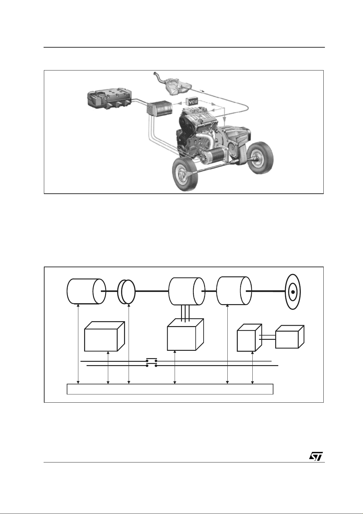
Figure 1: Basic Architecture of a Parallel HEV
Fig.1 depicts the basic arc hitecture of a parallel HEV. Parallel means that the mechanical p ower of ICE
and that of the e lectric mo tor are added in parallel to prov ide torque t o the wheels. For a s hort distance,
pure electric mode is possible. For a long distance, ICE provides the necessary autonomy. When a peak
transient torque is required to boost the vehicle, the two torques are added.
Fig. 2 reports the functional schematic.
Figure 2: Functional Schematic of a Parallel HEV
Internal
Combustion
Engine (ICE)
HV Battery
Clutch
Electric
Machine
CONTROL
Inverter
HV BUS
Gearbox
DC/DC
Converter
Wheels
LV
Battery
The suggested imp rovement has been o btained in the inverter block which houses the active s witches
required to drive the electric motor.
Main goals for power electronic equipment in electric vehicles are: low cost, high reliability and low total
volume. It is a true cha llenge. In terms of cost and reliability, there is a huge gap bet ween low-cost and
2/8

Obsolete Product(s) - Obsolete Product(s) Obsolete Product(s) - Obsolete Product(s)
AN1597 - APPLICATION NOTE
highly reliable standard discrete plastic packages for power transist ors and costly high power modules.
These modules usually exhibit lower reliability due to complex assembly and low volume production.
For surface mount devices, this gap is even larger. Particularly for low-cost applications, module
techniques are not suitable. On the other hand high-volume automotive applications require an AQL
(Average Quality Level) of < 1 ppm and extremely low-cost devices.
A new surface mount plastic package, using m ass -production t ooling able to house l arge dies (c a. 300 x
400 mils
cost reduction by lowering the labor cost for assembly and will increase reliability by improving the
process control. This assembly technique is modular and gives more independence from module
suppliers.
In this paper we show a new module using surface mount technology. The module has been realized
thanks to a new specially designed IGBT housed, toge ther with a high-speed diode, in a high-power
plastic package. This solution realizes a complete bi-directional current switch component with high
reliability and low cost mass production. The c omplete m odul e, rea lized with IM S technol ogy us ing 2 x 8
Max247 in parallel,it is a 400A, 600V power arm bridge unit for automotive applications.
This work has been developed within the INMOVE (Integrated Modular electric propulsion system for
parallel hybrid Vehicles) project founded by EC BRITE EURAM.
2
), will dramatically r educe the package cost. In addit ion, surface mounting will bring addit ional
3. Overview of the Device Technology
The elemental devices are punch-thro ugh IGBTs (PT-IGBTs) with a breakdown v oltage of 600V (50 A
rated current). The devices belong to the last IGBT generation which are manufactured in the mesh overlay technology, i.e. a strip-based concept realized from a p-doped mesh st ructure (the body of th e IGBT )
where directly diffused n+ doped strips substitute the cells, and represent the emitter of the IGBTs.
This particular technological solution allows the IGBTs to be easily made with a reduced on-state voltage
drop through a reduct ion of the on-s tate resistance (up t o 20 % ). Moreov er, the presence of a deep body
p+ avoids the trouble of static latch-up, as the resistance of the bo dy extending under the n+ source is
reduced.
An improved ruggedness, useful fo r paralleling connections, has been reached by mean s of the ballast
resistance technique, by using an "H" type layout structure. The cross section of the manufactured
device with the ballast resistance is shown in Fig. 3.
The extension of the p+ layer over the metallic contact increases the path of the electron current, thus
creating a ballast resistance Rb. During conduction condition, the current through the source of
the MOSFET causes, through Rb, a negative feedback on the gate-source voltage, and the gain is consequently reduced.
3/8

Obsolete Product(s) - Obsolete Product(s) Obsolete Product(s) - Obsolete Product(s)
AN1597 - APPLICATION NOTE
Figure 3: Cross-section of a robust IGBT with ballast resistors.
Table 1 summarize s the typical static and dynamic performance of the complete switch (IGBT + Diode)
measured at room temperature.
Table 1: STGY50NB60HD typical values
BVdss @ 250µA 650V
Vth @ 250µA 3.5V
Vcesat @ 50A 2.1V
Vfec @ 50A 1.55V
rise time @ 480V , 50A 50ns
fall time @ 480V,50A 150ns
Eoff @ 480V,50A 1.1mJ
Irm 7A
trr 60ns
4. 400A Module Design
During the INMOVE project a 600V, 400A power module was designed and built for th e conv erter of the
electric propulsion unit according to the guidelines suggested by the investigation carried out on efficiency, reliability, total volume, cooling requirements and cost.
The topology of t he inverter is a conventional ha rd switching B6-configuration cons isting of three halfbridges with an internal free wheeling diode. E ach half-bridge must be capable of ha ndling up to 600V
and 400A.
4/8

Obsolete Product(s) - Obsolete Product(s) Obsolete Product(s) - Obsolete Product(s)
AN1597 - APPLICATION NOTE
A viable way to obtain high current switches is to connect in parallel several rather small devices. The
design of a power switch able to handl e 400A pea k current needs the paralleling techniques to be used
at different levels: devices, connections (electric, thermal and mechanical), driving circuit. The pract ical
manufacture of such a switch needs various problems to be solved in terms of active switches characteristics, stray inductance equalization, power terminal connections and heat transfer.
The design of a power switch module for 400A, using paralleled devices, needs to determine:
- Selection criteria of devices working together in the same module to obtain a good current and
losses share between each component and this for the whole range of the functional area.
- Module structure (switch, bridge-arm, full-bridge) to minim ize the parasitic effects due to the paralleling
topology.
- Technological elemen ts (electrical isolation, thermal requirements, mechanical ruggedness).
A detailed analysis of all these aspects is reported in Reference 5. The module has been realized according to the obtained results and using STGY50NB60HD devices connected in parallel and assembled on a
low cost support like IMS (Insulated Metallic Substrate). Refer to Fig.4 for the electrical scheme.
The main characteristics of the final module are summarized hereafter:
- Size 150 x 83 x 18 mm
- Assembly on IMS substrate BERQUIST THERMALCLAD whose characteristics are:
- Base layer 3.2mm Aluminium 6061 T6;
- Dielec tr i c l a y e r 75µm
- Circuit layer ED copper 140µm
- Thermal Resistance 0.65 °C cm
- Capacitance 70 pF/cm
2
2
/Wat t
- The active switch is the STGY50NB60HD. It is a 600V, 50A fast IGBT assembled with an antiparallel
diode in a new Max247 plastic packag e. The devices are selected, at room temperature, according to
∆Vcesat @ 50A < 150mV; ∆Vf @ 50A<100mV; Idss @ 600V < 20µA.
- Power connections with screw terminals for each 100A arm, control connections with plug terminals
- An individual 10Ω series resistance is present for o scillation dumping, w hile a 10KΩ resistor with two
18V zeners, connected back to back, form the gate protection. An individual Kelvin path is required on
the emitter for fast driving, while a desaturation sensing connection is used for devi ce over-current protection.
5/8

Obsolete Product(s) - Obsolete Product(s) Obsolete Product(s) - Obsolete Product(s)
AN1597 - APPLICATION NOTE
Figure 4: Schematic of 600V, 400A IGBT Module
Tr1..Tr16 =STGY50NB60HD
R1..R16=10
R17..R18=10KΩ
Dz1..Dz4=18V
Ω
HT+
GATE
DRAIN
SOURCE
GATE
DRAIN
SOURCE
C2
3
2
1
C1
3
2
R17
R18
Dz2
Dz1
Dz3
Dz41
TR1
R1 R2 R3 R4 R5 R6 R7 R8
TR9 TR10 TR11 TR12 TR13 TR14 TR15 TR16
R9 R10 R11 R12 R13 R14 R15 R16
TR2
TR3 TR4 TR5 TR6 TR7 TR8
0
HT-
Fig. 5 shows the final assembly: the four 600V, 100A arms will be connected in parallel by a bus bar fixed
by screw.
The power modul e has been electrically characterized at different case temperatures. Table 2 summarizes the values of relevant parameters measured on typical devices. Table 3 reports the thermal resistance.
The application of these new 400A half-bridge power modules has been performed within a power
inverter. This inverter controls and supplies a permanent magnet synchronous motor of 30 kW, which
serves as additional traction drive for a hybrid vehicle.
Besides the reliability requirement of the automotive application, a cost optimization is also needed.
Therefore, it is important to take advantage of the peak voltage ratings of a power modul e t o achieve an
economic utilization of device voltage curren t ratings.
In order to utilize the voltage ratings up to the limit, minus a certain safety margin, a low inductive design
of the DC link is required to reduce voltage transients, caused by the IGBT switching, to a minimum. This
has been performed by a compact design with short electrical interconnections and a plane busbar (parallel arrangement of two isolated c opper layers), that di stributes both poten tials (+ and -) of supply v oltage between buffer capacitors and all IGBT power modules. The inverter has been prototyped within an
aluminium housing with int egrated water-cooling system in the bottom pa rt.
6/8

Obsolete Product(s) - Obsolete Product(s) Obsolete Product(s) - Obsolete Product(s)
Figure 5: Photo of the 600V, 400A Power Module Prototype
Table 2: Power Modules Relevan t Parameters
AN1597 - APPLICATION NOTE
25°C 125°C
Vcesat@400A 2.2V 1.9V
Vfec@400A 1.6V 1.5V
Eon@300V,400A 9.8mJ 11.0mJ
Eoff@300V,400A 7.3mJ 14.4mJ
Table 3: Thermal Resistances
Rth up down
IGBT 0.107°C/W 0.111°C/W
Diode 0.137°C/W 0.127°C/W
5. Conclusions
In this paper we present a new possibility to realise power m odules using standard plastic packaging
devices associated in parallel with IMS technology. The main advantages of this new power module
design can be summarized especially focusing on the automotive appl ication:
- Low profile design.
- Increased reliability regarding automotive temperature levels (thermal fatigue)
- Vibration and shock requirements
- Flexibility in current ratings without significant tooling costs, (scaleable design: 50A, 100A, 150A,..)
- Cost reduction on custom specific redesigns
7/8

Obsolete Product(s) - Obsolete Product(s) Obsolete Product(s) - Obsolete Product(s)
AN1597 - APPLICATION NOTE
A first production cost estimation for quantities of ten thousand parts/year has not yet resulted in a
competitive pric e level, if compared to conventional power mod ules. Improved relia bility may result in
slightly increased costs, but subsequent investigations should show cost reduction, especially if
production processes for high quantities will be investigated in detail.
REFERENCES
[1] R.Letor, "Static and dynamic behaviour of Paralleled IGBTs". IEEE Transactions on Industrial
Applications vol.28, NO2, MARCH/APRIL 1992, p.395-402.
[2] D.Medaule, Y.Yu: "Parallel operation of high power IGBTs". IEE Colloquium, London 25th April 1995.
[3] P. Hofer-N Oser, N. Karrer: "Monitoring of paralleled IGBT/Diode Modules: IEEE Transactions on
Power Electronics, Vol.14, NO.3, MAY 1999, p438-444.
[4] PO.Jeannin, M.Akhbari, JL.Schanen: " Influence of stray inductances on current sharing during
switching transition in paralleled semiconductors". EPE’99, Lausanne.
[5] D.Lafore, J.Legeleux, M.Melito, L.Fragapane, A.Ruethlein: "New Design for High Current Power
Modules Using Max247TM Package with IMS Substrate:Automotive Aplication". PCIMUSA2001,
Rosemont (IL).
Information furnished is b elieved to be accurate a nd reliable. Howe ver, ST Microelectronics a ssumes no resp onsibility
for the consequences of use of such information nor for any infringement of patents or other rights of third parties
which may result from its use. No license is granted by implication or otherwise under any patent or patent rights of
STMicroelectronics. Specification ment ioned in this p ublication are subject to change without notice. This pub lication
supersedes and repla ces a ll information pre viously su pplied. STM icr oelectro nics pr oducts are not authorized for use
as critical components in life support devices or systems without express written approval of STMicroelectronics.
The ST logo is a registered trademark of STMicroelectronics
© 2002 STMicroelectronics - Printed in Italy - All rights reserved
STMicroelectronics GROUP OF COMPANIES
Australia - Brazil - China - Finland - France - Germany - Hong Kong - India - Italy - Japan - Malaysia - Malta - Morocco -
8/8
Singapore - Spain - Sweden - Switzerland - United Kingdom - U.S.A.
http://www.st.com/pmos
 Loading...