

Page 1
AN1596
®
- APPLICATION NOTE
VIPower: HIG H SIDE DRIVERS FO R AUTOMOTIVE
V. Graziano - L. Guarrasi - A. Pavlin
INTRODUCTION
Today’s automotive market requires a continuous increasing of complexity and reliability in the electronic
systems. To achieve this, the concept of the automotive systems is more and more based on micro
controllers architec ture driving integrated monolith ic circuits that include a power stage, control , driving
and protection circuits on the same chip. Vertical Intelligent Power, a STMicroelectronics patented
technology, est ablished over 13 ye ars ago, uses a f abrication pr ocess which allows the integration of
complete dig ital an d/or ana log co ntrol ci rcuits driving a vertic al pow er trans istor on the s ame ch ip. The
VIPower M0 technol ogy used for makin g High Side Driv ers (HSDs) prod uces a monolithic silicon chip,
which combines control and protectio n circuitry with a standard powe r MOSFET structure where the
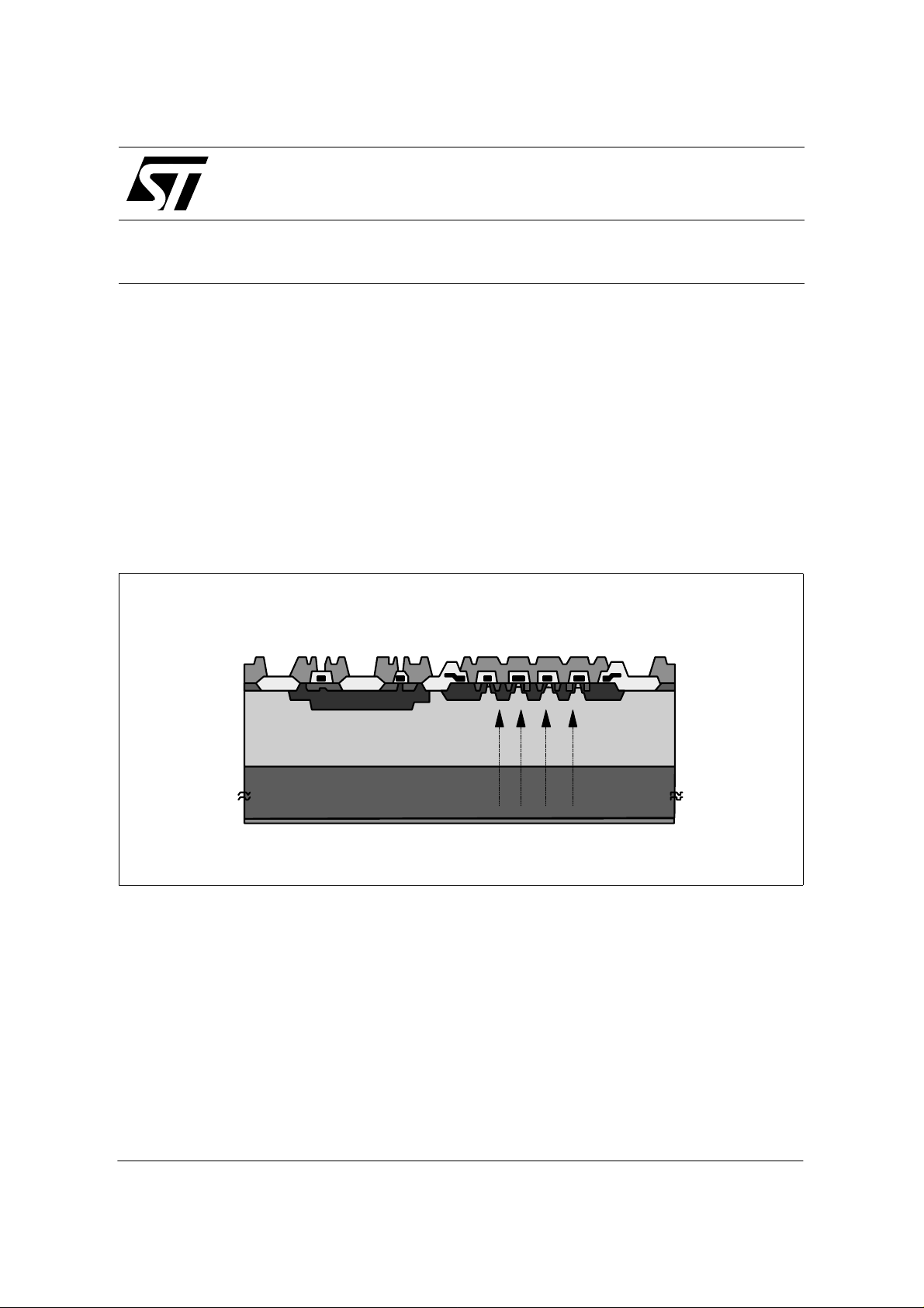
power stage current flows vertically through the silicon (see figure 1).
Figure 1: M0 chip structure
Drivin g ci r cu itr y
Enhancement and depletion NMOS
Power stage
VDMOS
p - well
n - type epilayer
n + substrate
Power st a ge out put
The evolution of M0 tech nology made the drastic reductio n of die si ze and o f the res istanc e of devic es
possible during conduction as well; each generation has seen a significant (from 40% to over 50%)
decrease in specific on-resistance and this translates into die size reduction, smaller packages, reduced
power dissipatio n and hence cost effecti ve solutions. The third ge neration - the M0- 3 - is in production
while STMicroelectronics is now developing the M0-4 and M0-5 technologies which will allow to achieve
less than 5mΩ R
are power switches that can manage hi gh curr ents an d work up to about 36V su pply voltage. They only
require a sim ple TTL logic input a nd incorporate a diagnostic output to th e micro-controll er. They can
drive an inductiv e load without th e need for a freewhee ling diode. For complete prot ection the devic es
have an over-temperature sensing circuit that will shut the chip down under over-temperature conditions.
Due to the aggre ssive automoti ve environment , High Side D rivers are de signed to w ork from -40 °C to
+150°C. They also have an under-voltage shutdown feature. Each application exerts an external
November 2002 1/24
in a PowerSO-10 package. High Side Drivers, with their integrated extra features
DS(on)
Page 2
AN1596 - APPLICATION NOTE
influence over the switch. A filament lamp or DC motor, for example, has in-rush currents that any switch
needs to h andle. So lenoids and moto rs h ave an ind uctive e ffect a nd must lose th e resi dual magne tism
when the curr ent is turned of f. Extern al fault condition s can also str ess the dri vers and their associat ed
circuitry. Th e M0-3 High Side Dr iver can be di vi de d in An alog and di gital . This c lass ific ation is do ne wi th
regard to diagnostic pin, which can be a two level signal pin or an analogue current sense pin. Diagnostic
information outp ut helps the on Board mi crocontroller to qui ckly identify and isolate faults saving repai r
time and often improving safety. High Side Drivers can reduce the size and weight of switch modules, and
where multiplexed systems are used, they dramatically reduce the size of the wiring harness.
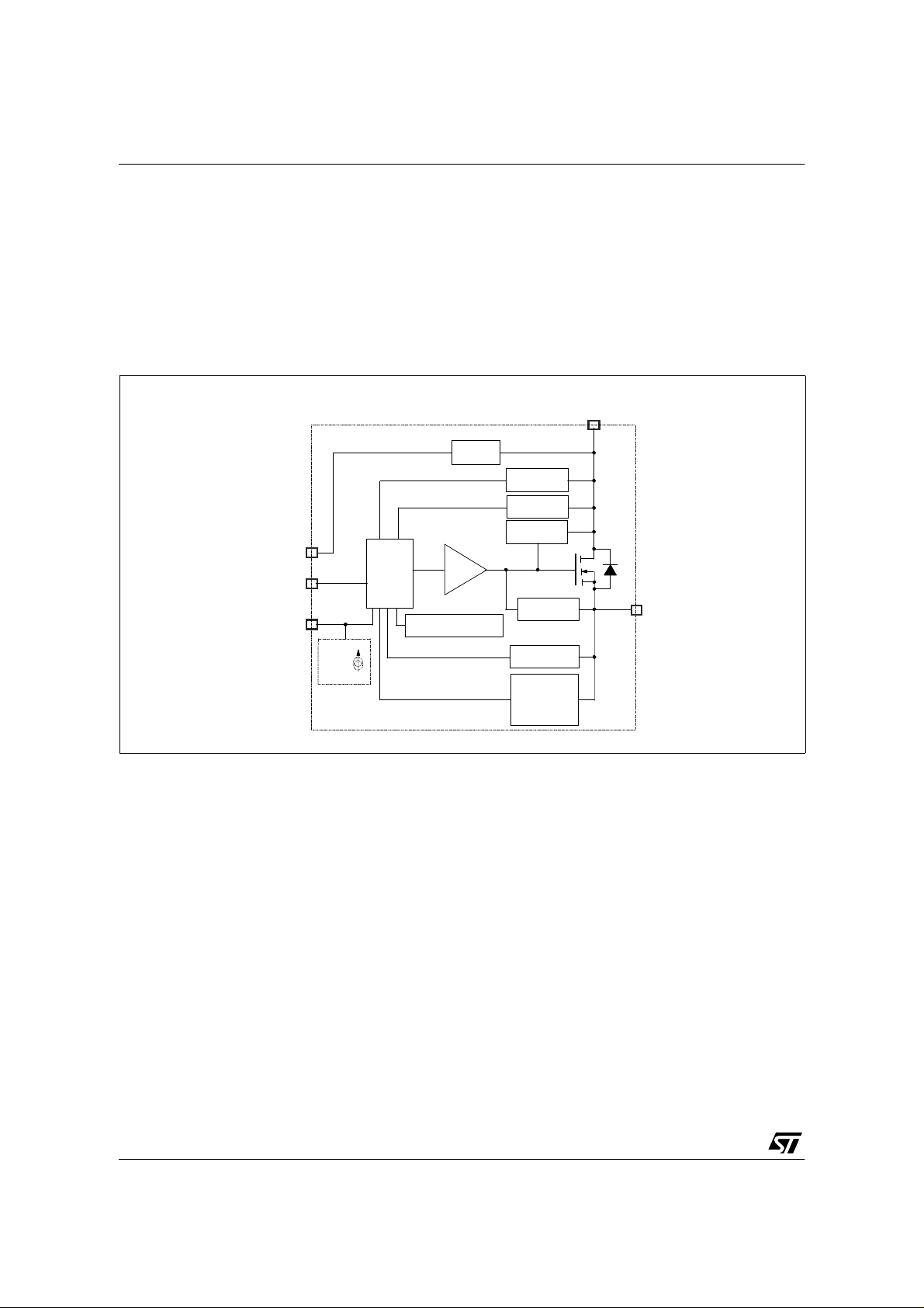
Figur e 2: Generic HSD Internal Block Diagram
Vcc
Vcc
clamp
OVERVOLTAGE
UNDERVOLTAGE
Power
CLAMP
GND
GND
Input
Status or
Current
sense
Isense =
OUT/K
I
Logic
DRIVER
OVERTEMPERATURE
Current
LIMITER
OPENLOAD
ON STATE
OPENLOAD
OFF STATE
&
Vcc/OUT
SHORTED
OUT
STMicroelectronics HSDs are designed to provide the user with simple, self protected, remotely controlled
power switches. They have the general structure as shown in figure 2.
THE GENERAL FEATURES OF HIGH SIDE DRIVERS
Input
The 5V TTL input to the se High Side Drivers i s protected agai nst elec trostati c discharg e (V
control pins an d 5kV for P ower pins ) . Gener al rules conc e rning T TL log ic sho ul d be app lie d to the inp ut.
The input volta ge is clam ped inter nal ly at V
a higher input voltage using an external resistor calculated to give a current not exceeding IIN=10mA (see
=6.8V as typical value. It is possible to drive the input with
ICL
ESD
=4kV for
datasheets absolute maximum ratings section).
Internal power Supply
To accommoda te the wide supply voltage ra nge experienced by the l ogic and control functi ons, these
devices have an internal power supply. Some parts of the chip are only active when the input is high, the
charge pum p for e xample. Therefo re it i s poss ible to conserve p ower when the device i s idl e. The new
M0-3 generat ion High Side Drivers supply cur rent in the ON state is 5mA/channel. Th e internal power
consumption for the basic functions of the chip under any circumstances - even when the input is 0V - is
very low. The supply quiescent current IS, guaranteed at junction temperature of 25°C, a ba ttery volta ge
2/24
Page 3
AN1596 - APPLICATION NOTE
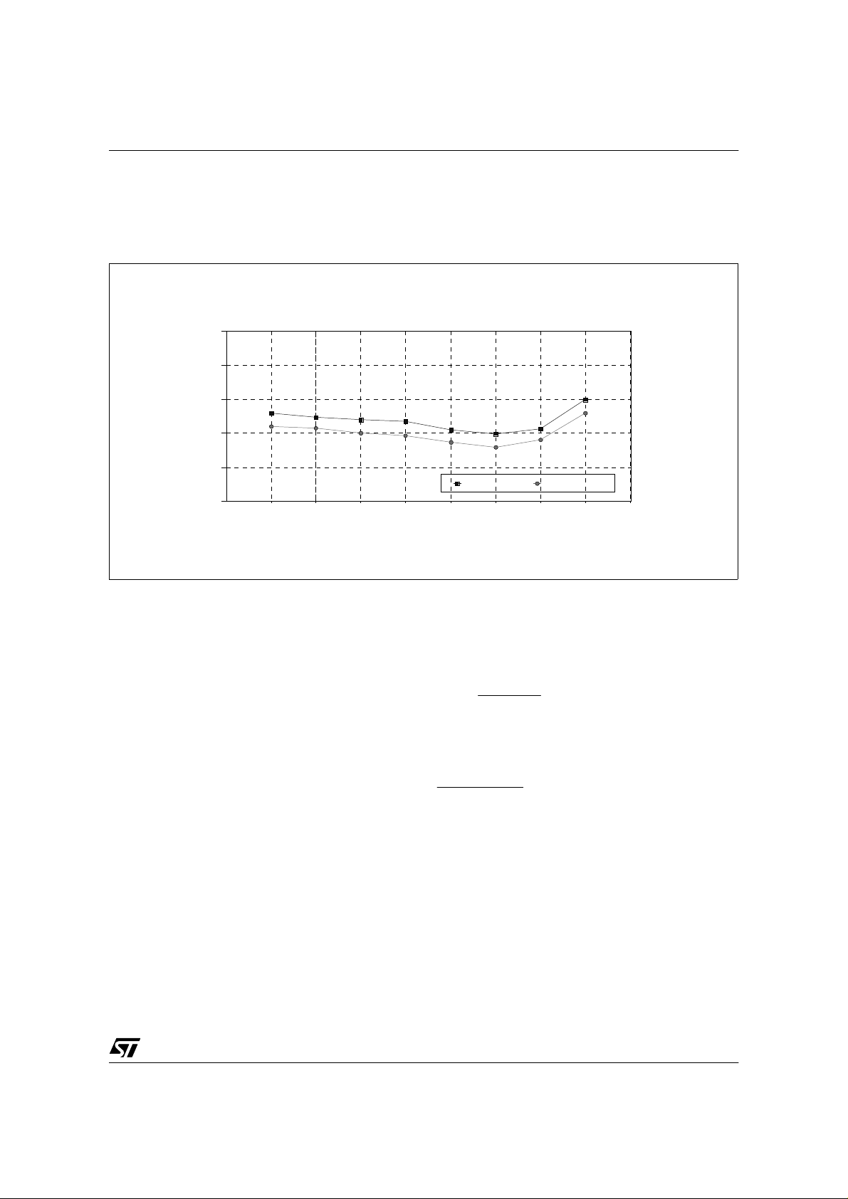
of 13V and the output pin grounded, is limited to a typical value of 10µA for a one channel HSD. In figure
3 a plot of typical IS values versus Tj is shown for single channel and double channel monolithic HSDs.
Figur e 3: Stand-by current for single and double channel single chip HSDs Vs. junction temperature
Is(uA)
25
20
15
10
5
Double channel Single Channel
0
-50 0 50 100 150
Tcase(ºC)
Thermal considerations
In order to choose the s uitable HSD for a given load s ome impo rtant po ints mu st be hi ghlight ed. In t he
worst-case operation (Tj=150ºC), for a single channel HSD and in steady state conditions, the Joule effect
power developed by the device equals the Power dissipated according to the following equation:
TT
2
)(
IVIR
SCCOUTonDS
Assuming that the second term can be neglected, for a given load current I
sink and a given ambient temperature (fixed at 85°C in automotive environment) the result is:
()
150
CR
)(
onDS
This is the maximum value of R
function of the junction temperature and in the datasheet its value is given at 25°C and this is
which can be chosen. The steady state on-resistance of HSDs is a
DS(on)
=°
2
approximately doubled at 150°C. In some cases it may be convenient to use an HSD with a bigger R
in the same package. To still comply with the above equation we must reduce R
heatsink. The trend from through-hole packages to low-cost SMD applications has led to think of the PCB
−
=⋅+⋅
−
RI
⋅
ambJ
R
ambthj
−
a given package and heat
OUT
TT
ambJ
ambthjOUT
−
and have a better
thi-amb
DS(on)
as a heatsink itself. In earlier packages (like PENTAWATT) a solid heatsink was either screwed or
clamped to the po we r packa ge and it was easy to calcul a te the th erm al resis tan ce from the ge ometr y of
the heatsink. In SMDs the heat path must be evaluated: chip (junction) - leadframe - case or pin - footprint
- PCB materials - PCB volume - surroundings. To evaluate static thermal properties of an SMD an
associated stati c equ iva lent ci rcuit (s ee figur e 4) can be c onsider ed. The power dissipation of the chip is
symbolized by a c urrent source whi lst the ambient temperature is represented by a vol tage source. By
estimating the PCB heatsink area in a real applica tion, the user can easily determin e R
thj-amb
in still air,
3/24
Page 4
AN1596 - APPLICATION NOTE
which is the worst case; in re al applications the values for the heat resistance are much lower. T he
following equation applies:
TTR−
ambj
P
V
Figur e 4: Static thermal equivalent circuit
=
−
ambthj
Rthj-amb
Die
d
P
In the above equation, the power loss PV and the ambient temperature T
a temperatur e chamber. The chip temperatur e Tj can be derived dur ing the operation, meas uring the
device’s R
Figur e 5: PowerSO-10 recommended layout for high power dissipation capability
DS(on)
j
T
= (VCC - V
OUT
Die Bond
R
thj-case
)/I
OUT
Lead-frame
Solder
R
Tcase
.
Heatsink
thcase-amb
amb
Tamb
can be easily determined in
Rthjamb = 50 C/W Rthjamb = 35 C/W
recomended pad layout pad layout + 6 cm2 on board heat sink
4/24
R
thjamb
= 20 C/W R
thjamb
= 15 C/W
pad layout + ground layers pad layout + ground layers + 16 via holes
Page 5
AN1596 - APPLICATION NOTE
Having the characteristic R
different PCB layout for PowerSO-10 package. The thermal resistance R
50°C/W to 15°C/W by holes linking different copper layers.
versus Tj, the relevant chip temperature can be derived. Figure 5 shows
DS(on)
can be reduced fro m
thj-amb
In the VIPower H SDs dat asheet s there are two section s concer ning th e thermal ma nagement. The fi rst
one shows the thermal calculation in order to find out the junction temperature in static conditions together
with a plot of thermal resistance junction to ambient versus PCB heatsink area. The second one shows a
plot of thermal impedance junction ambient in single pulse and the thermal model is shown with relevant
thermal resi stances and cap acitors values ( easy simu lations ca n be per formed bo th in st atic cond itions
and during transi en ts as , for exam ple, s wit ching on a l oad wi th high i n rush curren ts or PWM operation).
In figure 6 an example of a double channel HSD thermal model is shown.
Figur e 6: VND830 (SO16L package) thermal model
Area/island (cm2) Footprint 6
R1 (°C/W) 0.15
R2 (°C/W) 0.8
R3 (°C/W) 2.2
R4 (°C/W) 12
R5 (°C/W) 15
R6 (°C/W) 37 22
C1 (W.s/° C) 0.0006
C2 (W.s/°C) 2.10E-03
C3 (W.s/°C) 1.50E-02
C4 (W.s/°C) 0.14
C5 (W.s/°C) 1
C6 (W.s/°C) 3 5
Tj_1
Pd1
Tj_2
C1
C1 C2
R1
Pd2
C3 C4
R3R1 R6R5R2
R2
R4
T_amb
C5 C6C2
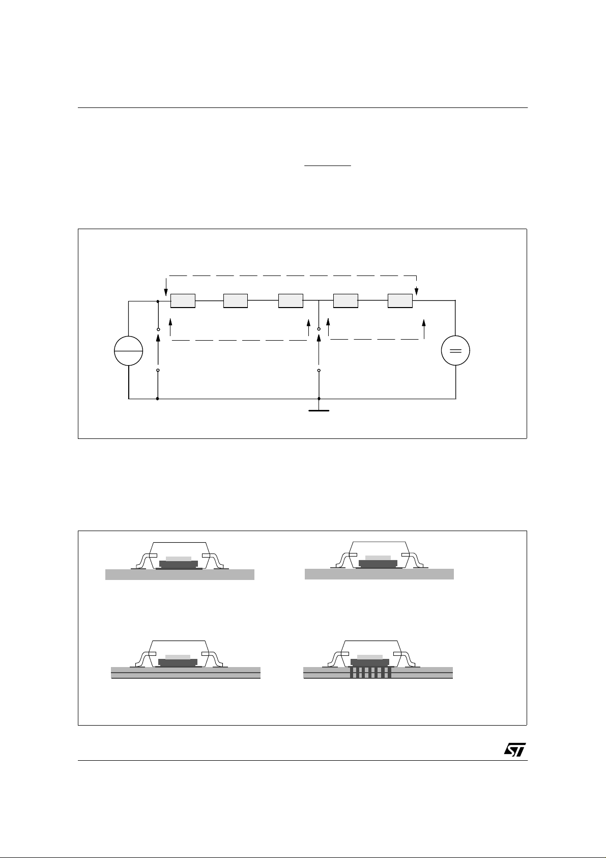
THE CONTROL AND PROTECTION CIRCUIT
Protection against low energy spikes and load dump
The voltage tra ns ients ar e v ery d ange rous hazards to the au tomo tive el ectro ni cs. The transients tend to
be either low energy- high voltage spikes or high energy-high voltage, up to 125V levels. The low energy
spikes are ge nera ted by fas t tu rnof f of hi gh- curre nt i nductive loads, such as air -cond it ioning c om presso r
clutches. This effect, combined with inductive behavior of wires, causes an overshoot voltag e on the
devices VCC pin. M0-3 Hi gh Sid e Driver s have an intern al protec tion desi gned to clamp the low ener gy
spikes to 41V (VCC clamp bloc k in figure1). In thi s situation the e nergy can flow thro ugh the internal
MOSFET T2 that is turned on through an internal clamp circuit (see figure 7).
M0-3 High Side Drivers are designed to su ccessfully pass the 1, 2, 3a, 3b and 4 ISO-7637 standar d
pulses t est ( see table 1 c arr ied i n HS Ds datasheets as wel l) - si mula ti ng the l ow e nerg y v olta ge spikes.
These values must be added to the voltage battery (for cars about 13.5V) to obtain the actual voltage. The
N.5 ISO7637 pulse simulates the alternator load dump in the case of a Generator with an internal
impedance of 2Ω and d i ffere nt value s of m agnetic field of the exc ita ti on circu i t (see figur e 8 for the level
IV pulse); this occurs when the battery is disconnected whilst being charged by the alternator. The voltage
spike can reach duration of approximately ½ second and it is of high-energy nature because of the
alternator' s low source imp edance. Where a cen tralized clam p circuit is not pro vided or ISO7637 rat ed
devices are not used, an external zener Dld diode is necessary to clamp the transient voltage battery (see
figure 7). This is done bec ause an inter nal prot ection ag ainst load du mp would requi re a large r die size
and - therefore - higher cost than putting on a module level protection.
5/24
Page 6
AN1596 - APPLICATION NOTE
Figure7: VCC clamp circuit against low energy spikes
Protection circuit
T1
Power
T2
MOSFET
Vcc
Dld
Ground
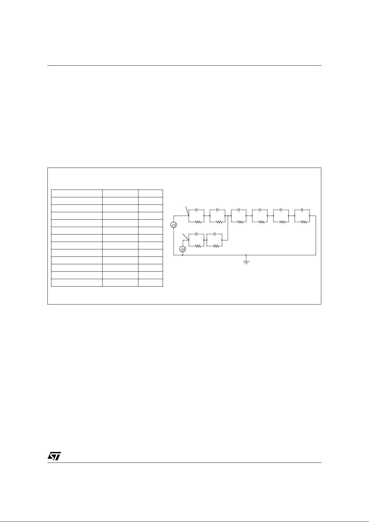
Table 1: Electrical transient requirements on VCC PIN
ISO T/R 7637/1
Test Pulse
I II III IV Delays and
1 -25 V -50 V -75 V -100 V 2 ms 10 Ω
2 +25 V +50 V +75 V +100 V 0.2 ms 10 Ω
3a -25 V -50 V -100 V -150 V 0.1 µs 50 Ω
3b +25 V +50 V +75 V +100 V 0.1 µs 50 Ω
4 -4 V -5 V -6 V -7 V 100 ms, 0.01
5 +26.5 V +46.5 V +66.5 V +86.5 V 400 ms, 2
Figur e 8: N.5 ISO 7637 pulse (level IV)
Tr < 10ms
Tr
R
i = 2
Ω
T
Output
TEST LEVELS
T=400ms
Impedance
Ω
Ω
6/24
90%
100V
10%
13.5V
Page 7

AN1596 - APPLICATION NOTE
max)(
600
onS
GND
I
mV
R ≤
GND
CC
GND
I
V
R
−
≥
GNDCCD
RVP2−=
Under and over voltage lockout
Under and overvoltage protections occur when the supply voltage drops or raises to minimum and
maximum le vels specified in the datashee t as V
simply turns of f, just because it wo uld not work properly. Th e undervoltage condi tion may occur when
turning on a car headlamp for example, which is a near short circuit. The inductive effect of wires (typically
1µH/m) generates an opposing voltage across the wire and the apparent supply voltage drops. The
current increase rate for an HSD is about 1A/ms for a short-circuited load and using a 5m length wire, the
induced voltage will not be large enough to reduce the supply voltage below 5.5V and - therefore - the
HSD switches on. The overvoltage contr ol circuit acts as a protecti on for the load against overvol tages
(VOV=36V and above that value the device switches off).
Reverse battery protection
Most auto manu facturers specify t hat any el ectronic d evice must be able to withstand a reverse batte ry
connection. T he exact magnitu de of the reverse voltage requir ement varies per m anufacturer, but t he
worst case seems to be -24V for 10 min. The maximum allowed value of the ground current during reverse
battery is -I
problem.
Solution 1: Resistor in the ground line (R
is an indication on how to dimension the R
and it is specified in the device's datasheet. There are two possible solutions to this
GND
only). This can be used with any kind of load. The following
GND
GND
and VOV. Under V
USD
resistor.
(1)
=5.5 V val ue the Po werMO S
USD
−
Power dissipation in R
during reverse battery situation is the following:
GND
(2)
()
This resistor can be shar ed amongst several different HSDs. In this case in the formula (1) I
becomes the sum of the maximum on-state currents of the different d evices. When the microprocessor
ground is not common with the device ground then the R
input thresholds and the status output values. This shift will vary depending on how many devices are ON
in the case of several HSDs sh aring the sa me R
with formula (1) and formula (2) may not be fulfilled. To overcome this problem, ST suggests the following
. This can lead to a very little value of R
GND
will produce a shift (I
GND
S(on)max
solution.
Solution 2: a diode (D
DGND if t he de vice drive s an ind uc tive l oa d (se e c hap ter about fast d emag netizati o n). T his sma ll signal
) in the grou nd line. A resistor ( R
GND
=1kΩ) should be inserted in parallel to
GND
diode can be safely shared amongst several different HSDs. Also in this case, the presence of the ground
network will produce a shift (~ 600mV) in the input threshold and in the status output values if the
microcontroller ground is not common to the device ground. This shift will not vary if more than one HSD
share the same diode/resistor network.
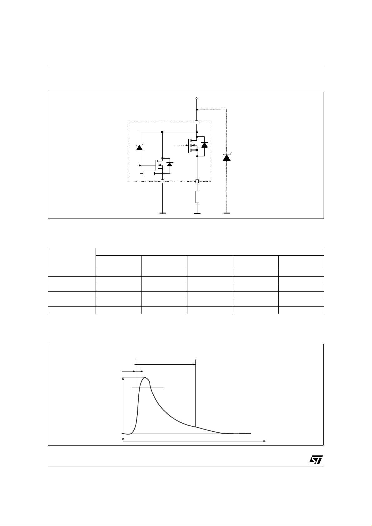
Micro-controller I/Os protection
If a ground protection network is u sed and negative transien ts are present on the VCC line, the HSD
control pins will be pulled negative due to parasitic in ternal structures. Th is may cause the microcontr oller
I/O pins to latch up. The value of the resistors (R
voltage shift from the mic ro-controller output to the HSD control pins, and the latch-up limit current of
) to be connected, is a compromis e between the
prot
micro-controller I/Os. The following condition must be fulfilled:
V −−
−
CCpeak
I
R
≤≤
lu
prot
µ
VVV
GNDIHCout
I
IN
Where:
-V
=negative peak voltage
ccpeak
* R
GND
S(on)max
) in the
GND
to comply
7/24
Page 8
AN1596 - APPLICATION NOTE
outonDSsensedsn
IRIR ⋅=⋅
)(
Ilu=µC's latch up current
V
=output µC's voltage
out µC
VIH=minimum input HSD high level
V
=voltage drop across ground network
GND
IIN=maximum input current
Figure 9 shows the external circuitry used for reverse battery protection and micro-controller protection.
Figur e 9: Ground and µC protection network
+5V
µ
C
R
R
prot
prot
+
5V
V
CC
STATUS
INPUT
HSD
GND
Vcc
OUT
Iout
Vout
GND
D
R GND
Over temperature protection
Over-temper atur e pro tecti on is based on sen s ing the c hip tem pera ture onl y. T he l oca tion of the sensing
element on t he chip in the pow er stag e area, e nsure s that accura te, ve ry fast , tempera ture detect ion is
achieved. Th e range within which over -temperature cutout occurs is T
output goes lo w with a maximum delay of only 20µs. Over-temperat ure protection acts to pr otect the
=150ºC minim um. The status
TSD
device fro m th erma l dama ge a nd l imi ts t he av e rage curr ent wh en sh ort ci r cuits occur i n th e load as well
(see chapter about abnormal load conditions).
Analog current sense
Some of the new HSDs made by using the VIPow er M0-3 technolog y have the curr ent sense featur e
(VN60, VN61, VN92 and VNC6 lines). This allows to develop a voltage signal - that is proportional to the
load current - across an external resistor R
principle of operation is to compare the currents flowing through two paths: the sense path made up of the
series of n-cells PowerMOSFET plus the sense resistor (I
of N-cells MOS plus the connected load (I
. In figure 10 the HSD current sense circuit is shown. The
sense
) and the power path made up of the series
sense
out
).
During the on-state condition the load current creates a voltage drop on the output pin; the OpAmp
compares the voltage drop across the Power MOSFET V
n-se nse MOSFET V
dsn=Rdsn
• I
; in normal operation V
sense
dsN=RDS(on)
dsn
= V
• I
OUT
, therefore:
dsN
to the voltage drop across the
8/24
(3)
Page 9

Figure 10: Current sensing internal circuit
KIRV
outsensesense
/
INPUT
DRIVER
+
LOGIC
I
sense
Sense
MOSFET
-
+
Power
MOSFET
Rsense
+ V cc
+VCC
AN1596 - APPLICATION NOTE
OUT
LOAD
I
OUT
Since V
sense=Rsense Isense
⋅=
, putting K = R
dsn/RDS(on)
(4)
, this expression yields:
Figure 11: VN920 current sense plot and calibration points
Vsense (V)
Vsense (V)
7
7
6
6
5
5
4
4
(Iout2, Vsense2)
3
3
(Iout1, Vsense1)
(Iout1, Vsense1)
2
2
1
1
0
0
012345678
012345678
(Iout2, Vsense2)
Iout (A)
Iout (A)
The sense resistor is chosen applying formula (4) in order to have the desired voltage value to be read by
the micro-controller A/D converter.
9/24
Page 10

AN1596 - APPLICATION NOTE
IR
V
outsense
sense11
=
b
R
VK
I
sense
sense
out
+
⋅
=
1
1
If a short ci rcuit occurs and the devi ce goes into thermal shutd own the sense voltage is pulled up at
V
SENSEH
delay of 500µ s. It is necessary to take into account that the K ratio may be influenced by some external
and physical parameters like the resistance of the bonding wire that goes from the PowerMOS pad to the
output pin RK or the juncti on te mper atur e and the b atter y v oltage . For the VN92 fam ily - for examp l e - K
spreads fr om 4400 to 5250 f or a fixed I
150°C. This application requires good sense accuracy, therefore it is necessary to decrease the K spread.
When I
key method consists in fix ing two load cu rrents in the linear zone and measuring the r elevant sense
voltages. During the measurement T
the output currents I
The K ratio is the angular coefficient of the straight line to the two measured points (see figure 11). In the
whole range of variation of the output current - we can suppose that:
Thus:
In order to calculate "b" and "K" we can solve the system of two equations (7) and (8) with the fixed values
of (I
value (given in the datas heets and typically 5.5V). The cur rent sensin g circuit has a maximu m
=10A and V
out
is in the range 1.5 - 6.5A, the sense voltage is proportional to the load current (linear zone). The
out
=25°C, R
out1
, V
sense1
out1
) and (I
and I
out2
K
, V
case
:
out2
⋅
V
; (5)
sense22
(7) ; (8)
).
sense2
Rb
sense
sense
=
⋅
K
senseout
I
=
out
2
RK
⋅=
sense
⋅=
=4V in a temperature rang e from 25°C to
sense
is fixed and VCC=13V. As explained before, given
IR
outsense
bIKI
+⋅=
VK
⋅
sense
2
R
−
VV
−
VV
−
+
sense
II
refref
1212sensesense
VIVI
⋅−⋅
1221
senserefsenseref
12
sensesense
(6)
b
(9)
(10)
An easy algorithm can give us the "K" and "b" values. During the final test of a module, the two pairs (I
V
ratio spread will be reduced of about 50%, even if the drift causes will still be present.
sense1
) and (I
out2
, V
) are store d in the releva nt HSD microc ontroller EEPROM. I n th is way th e K
sense2
out1
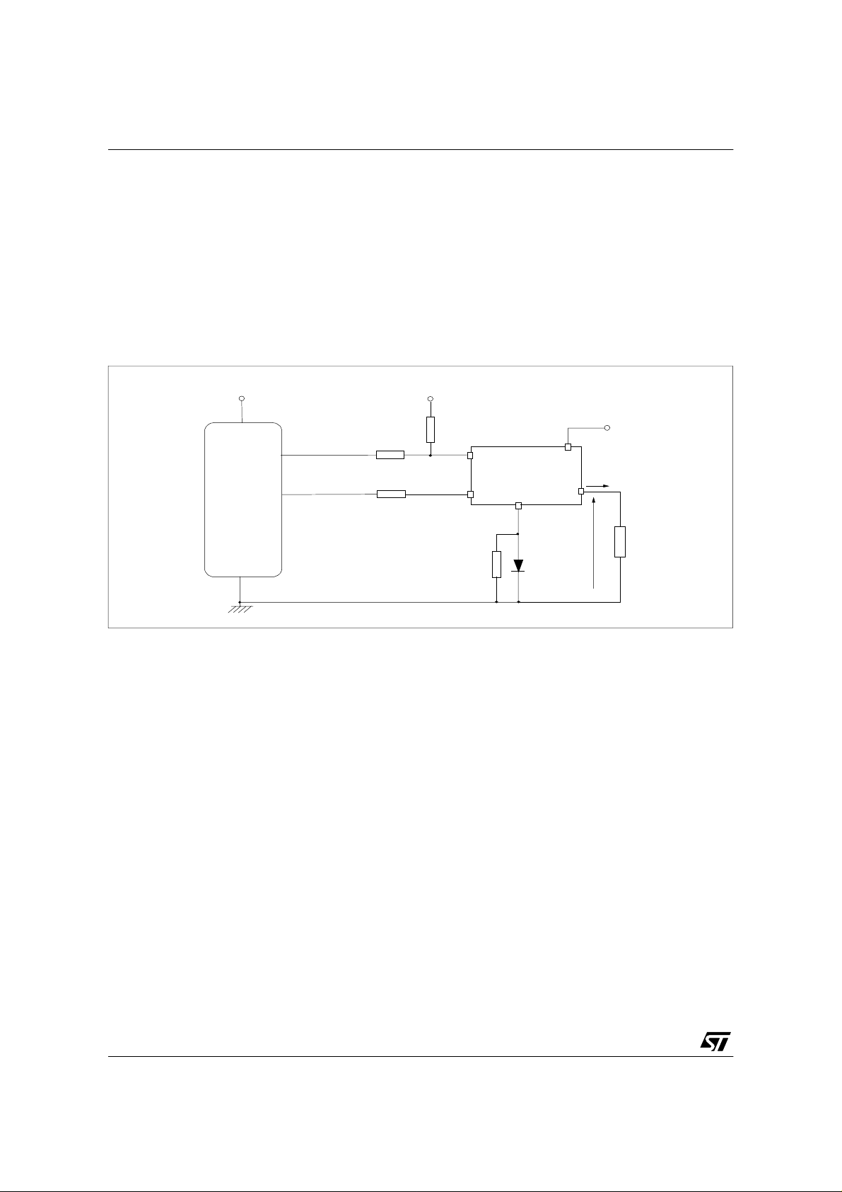
Open load detection (in ON and OFF state)
- Digital HSD
Open load detecti on occurs when the load becomes disco nnected. The M0-3 HSDs can provide lo ad
disconnection detection during the off-state as well as in the on state. In digital HSDs, during the ON state
a current I OUT flows through the pow er MOSFET (N cells M OS) and the load. The gate of a Sense
MOSFET (n cells MOS) is driven at the same time and the correlation between the currents flowing in the
two MOSFETs is the follo wing:
N
I ⋅=
I
n
senseMOSOUT
The internal circuit in figure 12 shows that if an open-load event occurs and the output current decreases
below IOL=K I
intervention threshold for VN75 is IOL=50mA).
value the status voltage goes low, signaling a fault (for example, the minimum
REF
The open load detectio n during switching on , has a delay of 2 00µs, indicated on the datasheets as
t
power stage; i n o rder to dete ct the ope n l oa d fau lt, an exte rnal resi stor is needed. In nor mal condition a
, whilst durin g ON sta te is ze ro. In th e OFF sta te condi tion, the current do esn't flow throu gh the
DOL(on)
certain current flows through the network made up of the pull-up resistor Rpu and the load (see figure 13)
10/24
,
Page 11
AN1596 - APPLICATION NOTE
and the voltage across is v ery lo w b ecause the load res istanc e is s u ppose d to b e much lower than p ull up resistanc e. If this vol tage stands below VOL threshold, an internal comparator will keep the status pin
in high impedence. If an open load occurs the output voltage is "pulled up" to a voltage close to the battery
and more than VOL value (maximum value 3.5V for M03 HSDs).
Figure 12: Open load detection in ON state for digital HSDs
+ V batt.=13V
+VCC
INPUT
STATUS
DRIVER
+
LOGIC
-n-
cells
-N-
cells
OUT
OUT<IOL
I
REF
I
Figure 13: Open load detection in OFF state for digital HSDs
V batt. Vpu
+VCC
INPUT
STATUS
DRIVER
+
LOGIC
+
R
V ol
GROUND
OUT
I
l(off2)
LOAD
pu
R
LOAD
R2
GROUND
11/24
Page 12

AN1596 - APPLICATION NOTE
In the OFF state de tection th e delay is highe r than the delay in the ON state (ma ximum t
and maximum t
DOL(off)
=1ms).
DOL(on)
=200µs
The external pull-up resistor has to be selected according to the following requirements:
1) no false open load indication when load is connected: in this case we have to avoid V
than V
2) no misdetection when load is disconnected: in this case the V
results in the following condition
The values of V
datasheets. The need of the pull up resistor for any single HSD channel means power consumption even
when the car is idle and a considerable increase of I
to avoid this, two ways can be chosen:
; this results in the following condition:
OLmin
V <⋅
OUT
Olmin
, V
Olmax
and I
L(off2)
V
pu
=
RR
+
puL
<
pu
I
VR
minOLL
has to be higher than V
OUT
VVR−
max
OLpu
)2(
offL
are available in the electrical characteristics section of
parameter from a few µA to several mA. In order
S(off)
to be higher
OUT
OLmax
; this
1) An external circuitry made of two transistors and two resistors.
Figure 14 shows a circuitry made of two transistors T1 and T2 connected in such a way that the collector
of T2 drives all the pull-up resistors connected to different outputs of a four channels HSD (VNQ type). In
this case the mic ro con trol ler can simply chec k al l the conn ec ted loads per iodi call y fo r a very short t ime
when the ignition key of the car is in. The bipolar transistors are cheap signal transistors.
Figure 14: Open load detection with external pull up network
Vcc
Pull u p resist a nces
4 Channels HSD
INPUT
DRIVER
VOL
Loads
µ
C
T2
STATUS
Pull up disable
networ
T1
k
2) A software trick for bulbs.
It is possib le to detect an open load w ithout connecting t he p ul l-up resi stor and w ithout switching on t he
loads. This solution needs to implement some tricks by software. The Micro controller can periodically
send a pulse to the input pin with a very short pulse width (for example 250µs). In this condition the HSD
is switched on but the co nnect ed lamp can not be hea ted up in such a short ti me. In a ddition the st atus
12/24
Page 13

AN1596 - APPLICATION NOTE
voltage can go low and signaling an open load condition (we remind that in ON state the status signal has
a maximum delay of 200µs).
- Analog HSDs
In the previous chapter the current sense feature in M0-3 HSDs has been shown; this is active during the
ON state only (INPUT=high) whilst in the OFF phase (INPUT=low) the current sense circuit is inactivated.
This means th at it is possible to detect an open l oad in ON state f ault but not during OF F state. Two
possible solutions can be thought of:
Solution 1: external comparator (see figur e 15 ). Eac h load i s conn ec ted to a pull u p r esi stor suppl ied by
the VCC line t hrough the networ k ma de of T 1 and T2. T he extern al com parator is n eeded to detect t he
voltage drop across the load and to compare it to a reference voltage (V
event occurs, the output pin voltage is pulled up to the VCC value and the comparator provides the microcontroller with the fault signal. As seen for digital HSDs, the pull up disable network is supplied when the
ignition key is in, but the car is off.
Solution 2: two additiona l signal bipolar tra nsi stor T 3 and T4 c a n be use d (see fi gure 16). The e mi tter of
the T4 transistor (PNP type) is connected to a positive 5V line, and its base is connected to the HSD input
line. This means that T4 is off when the HSD is on whilst it is on when the HSD is off. T3 (NPN type)
collector is conne cted to the T4 one while T3 base to the output pin. T3 doe sn’t conduct until the output
voltage (referr ed to ground) reaches its thresho ld value (VBE). This is the case of normal condition i n
which the voltage drop on the load is almost zero.
When an open l oad fault oc curs, the v oltage on the input pin ris es to the VCC value. In this condition T3
conducts and a voltage of about 5V appears on the sense pin. Therefore the micro-co ntroller will detect
the open load fault in OFF mode.
in the scheme). If an open load
ref
Figure 15: Open load cicuitry for analog HSDs (OFF state) with an external comparator
4 Channels HSD
INPUT
DRIVER
SENSE
C
µ
T2
+V ref.
Pull up disable
T1
Vcc
Loads
13/24
Page 14

AN1596 - APPLICATION NOTE
F
F
R
I
R
I R R I
I R I R
I R
I R
Figure 16: External circuitry for open load with two additional bipolar transistor T3 and T4
+Vcc line
T2
+5Volts
Pull-up disable network
T4
µ
C
T1
T3
IN
SENSE
DRIVER
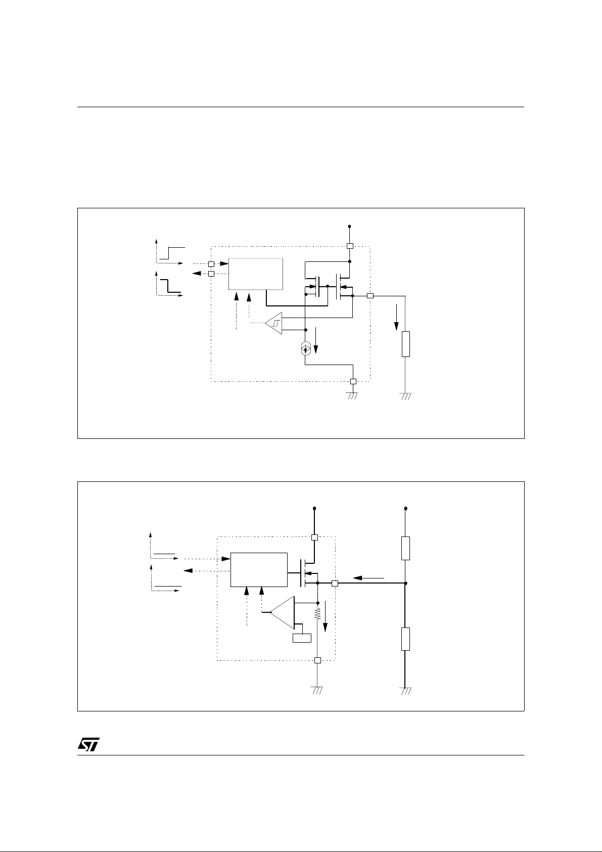
Voltage drop limitation feature
In the pre vious cha pter, w e high l ighted the open load detectio n fea ture for High Side Dr ive rs wi th digi tal
diagnostic feature and analog current sensing as well. For digital ones, in the ON state condition an
internal amplifi er compares the voltage drop VDS on the Power M OSFET du e to the lo ad cur rent to t he
voltage drop on the i nternal S ense MOSF ET (see figur e 12). Its output drives a c ircuitry ab le to give an
open load signal fault or a sense voltage across R
The High Side Drivers built by using the VIPower M0-2 technology (all with digital diagnostic), have a V
proportiona l to the load cur rent (figur e 17). This mea ns that in the low output curren t range, the v oltage
between drain and source has the magnitude comparable to the amplifier offset (V
the precision of open load detection becomes very low. At open load condition, the following equation can
(analog HSD).
SENSE
=5mV). Therefore
offset
DS
be written:
V
DS(on)
CC
OL
V
senseMOS
CC
± ⋅ − = ⋅ −
V
REF
offset
senseMOS
V
offset
DS(on)
⋅
V
offset
RE
m
V
⋅ = ⋅ =
K
RE
offset
m
DS(on)
=50mΩ, IOL= K I
DS(on)
=0.3A (typical). The
REF
DS(on)
senseMOS
OL
DS(on)
OL
m
REF
=
⋅
For example, let us consider an M0-2 HSD : VN21 with R
error on the voltage drop value due to the amplifier offset voltage is 5mV, and the formula (11) yields:
14/24
Page 15

AN1596 - APPLICATION NOTE
Figure 17: On resistance characteristics comparison between VN21 (M0-2) and VN750 (M0-3) HSDs
VDS(mV)
20
15
10
VN21
OL
!
OL
ε∗
I
I
OL
I
OUT
I
VDS(mV)
V
ON =
50
55
45
VN750
OUT
50mV/RDS (on)
OL
!
OL
ε∗
I
I
I
With a percentage error ε=33%. One of the advantages of the latest M0-3 digital HSDs, is the precision in
the load current read ing at low curr ent value as well. This is achieved by driving the gates of the Po wer
and Sens e M OSFET s in s uch a way as t o i ncr ease the on-state res ist an ces of both of the m a t low l o ad
current. The diagram in figure 18 fulfills this feature; it is a feedback circuit: when I
tends to be below VON=50mV, the internal amplifier allows the voltage gates (VGS) to go low and therefore
is low, and V
OUT
DS
to increase the on resistances of both MOSFETs. Then VDS goes up again to 50mV.
Figure 18: Voltage drop limitation circuit
INPUT
STATU S
Sense MOS
DRIVER
LOGIC
GND
+VCC
P MOS
+
+
-
V
DS
VON=50mV
OUT
LOAD
15/24
Page 16

AN1596 - APPLICATION NOTE
R
R
R R
R
R R
The resistanc e of the Power MOSFET does not have a lin ear behavior anymore (see figur e 17). It is
increased to the value RDS=VON/I
I
senseMOS
OL
DS
K ratio remai ns constant while RDS is increased . This allows a design that low ers the first addend of
equation (1 2), that’s to say the detection threshold. F or example, the VN750, a M0-3 digital HSD with:
R
=60mΩ, is designed in order to have IOL= K • I
DS(on)
At open load current the on state resistance RDS of the Power MOSFET is the following (see figure 4):
Much higher than the typical R
the following:
DS(ON)
- Analog HSDs
In case of H SDs wi th current sensing the beha vior of open load detec tion is simi lar; the Power and t he
Sense MOSF ETs are driven sim ultaneously in order to keep the differential signal above V
voltage drop limitation is VON=50mV too a nd is given in the protectio n section in the datasheets. T he
same equation (12) can be applied.
Note that for HSDs (digital and analog) the precision of current reading depends on I
HSDs) and the ratio K=I
OUT/Isense
> R
OUT
I
m
REF
. In this case, equation (11) becomes the following:
DS(on)
V
offset
DS
⋅ = ⋅ =
I K
REF
V
offset
m
REF
DS
at only 0.1A (typical).
(12)
RDS=50mV/100mA=500mΩ.
value of 6 0mΩ . In this case, from eq. (12), the open load reading is
IOL=0.1A±5mV/500mΩ=0.1±0.01A
=
I
OUT
= R
senseMOS/RDS(on)
senseMOS
DS
⋅
as well.
I
sense
V
offset
m
DS
(I
REF
sense
. The
offset
for analog
Turn off of inductive loads (fast demagnetization)
When an HSD turns off an inductance a reverse potential appears across the load. The energy stored in
the load during the ON condition has to be properly dissipated during switch off. The source of the Power
MOSFET bec omes more neg ative than t he ground and this can re ach the transi stor’s breakdown ( see
figure 19). To avoid this, the output has to be clamped at a certain demagnetization voltage, V
specific inductance. In this condition the inductive load is demagnetized and its stored energy is
demag
, of the
dissipated internally in the HSD. In the basic HSD family the typical value of the demagnetization voltage
is 4V. I n the M0-3 H SDs th e interna l ci rcuit c lamps t he voltage ac ross the Po wer MOS FET to a typi cal
value of 48V (given L=6mH, I
=2A) and, therefore the voltage across the load is:
OUT
48−=
VV
CCdemag
In this condition th e stored energy is re moved rapidl y in the Power M OSFET. The fast dema gnetiza tion
leads to sudden j unction tempe ratur e i ncrea se and, in case of rep etiti ve pulses , th is ca n cause chi p a nd
resin degradation.
If we suppos e that the induct ive load - which also has its resistanc e RL - is switc hed off once it has
reached the initial current I0, the shape of discharge current during the switch off is given by:
R
L
t
V
demag
ti
I
R
L
V
demag
−⋅+= 1)(
O
IR
⋅
OL
In the above equation, if we put i(t)=0, we can calculate the duration of demagnetization T
L
T ln
demag
⋅=
−
R
L
V
demag
⋅−
L
e
⋅
:
demag
⋅+−
IRV
OLdemag
16/24
Page 17

Figure 19: Switching off of an inductive load
AN1596 - APPLICATION NOTE
Turn on
OUT
GND
RGND
+
load
L
D
GND
load
OUT
I
V
-
Figure 20: Waveforms of fast demagnetization
VIN
Vcc
Turn off
GND
R
GND
D
GND
V
demag
OUT
Lload
-
load
I
Vcc
+
V OUT
I
OUT
Vcc
Vdemag
V
= 48 V
clam p
I (A) max b efore
turn off
t
t
t
17/24
Page 18

AN1596 - APPLICATION NOTE
The faster we want to switch off, the bigger has to be V
through the clamp circuitry during switch off is given by:
TT
demag demag
() ()
∫∫
00
R
+−
2
L
VV
CCdemag
+⋅⋅⋅
VIRL
demagOL
ln
VVdttiVVE
+−
VV
−
V
demag
compared with VCC. The energy dissipated
demag
R
L
V
demagCCdemagCCdemag
CCdemag
demag
R
V
demag
−⋅+⋅−=⋅⋅−=
I
1)(
O
⋅
IR
L
OL
t
⋅−
L
⋅
dte
=
The Power dissipated during turn off is:
E
P =
demag
T
demag
demag
In case of repetitive pulses, the average power dissipated in the HSD is given by the following expression:
δ
EfPP ⋅+⋅=
demagONav
Where:
δ = duty cycle
f = frequency
PON = power dissipated during ON state.
When an extern al signal diode is used as reve rse battery protec tion, an external resistor along wit h it
connected to ground pin is necessary ( see figure 19); in fact, during turnoff, th e ground pin pote ntial
becomes neg ative in comp arison w ith inp ut volt age and this mak es the P ower MOS FET tur n on ag ain.
Using R
(~ 1kΩ) the Ground pin potential is kept stable.
GND
ABNORMAL LOAD CONDITIONS
Short circuit (start-up with the load short-circuited and short circuit occurring during on state)
When a l oad beco mes short circ uited, various effects occur a nd c ertain step s ne ed to b e taken to deal
with them, particularly choosing the correct heat sink. Two clear cases of short circuit occur:
1)The load is shorted at start up
2)The load becomes short during the on state
At turn on the gate voltage is zero and begins to increase. Short circuit current starts to flow and power is
dissipated in the HSD according to the formula:
IVIVP
⋅≅⋅=
lim
CCOUTDSd
The effect is t o cause the silicon to h eat up. The po wer MOSFET s tays in the line ar region . When the
silicon temperature reaches a minimu m temperature of 150°C, the ove r temperature detectio n operates
and the switch is turned off. Passive cooling of the de vice occurs until the reset temp erature is reached
and the device turn s back on ag ain. Th e cycle is repet itive and stop s wh en the power is rem oved, wh en
the input is taken low or when the short circuit is removed. In this case the device controls the di/dt. Figure
21 shows a start up waveform when there is a short circuited load driven by a VN610SP. The initial peak
current is 45A for this 10mΩ device. Note that the sense pin is at high impedance during limitation phase
and is pulled up at about 5.5V during thermal shutdown. When a short circuit occurs during the on state,
the power MOSFET gate is al re ady at a hi gh volt a ge, abo ut VCC +8V, so the gate is hard on. Hence the
short circuit di/dt is higher than in the first case, and only controlled by the load itself. After the steady state
thermal condition is reached, thermal cycling is the same as in the previous case. After a certain time from
switching on, d epending on thermal i mpedance of the device, the first thermal shutdown oc curs. The
18/24
Page 19

AN1596 - APPLICATION NOTE
estimated ju nction temperatur e behavior ver sus time is sho wn in figure 22 fo r VN920SP with a current
limitation range of 30A-50A with 45A typical value.
Figure 21: Automatic thermal cycle at start up
Vin=5V/div
Vsense= 5V/div
Iout=30A/div
Figure 22: Junction temperature ve rsus time for VN920SP on 2.5 cm2 FR4 70mm thick fo r minimum,
typical and maximum limitation current
Tj vs time
Device: VN920SP
175
150
125
100
75
Tj (°C)
50
25
0
0.000 0.003 0.006 0.009 0.012 0.015
13V*50A
13V*45A
13V*30A
time (s)
Obviously, whe n the maxim um junction t emperature is fixe d, the high er the curren t limit, the fa ster the
thermal shutdown intervention.
19/24
Page 20

AN1596 - APPLICATION NOTE
Evaluating the average and RMS currents in short circuit condition
The thermal cycling in overload conditions produces repetitive current peaks. The device switches on, the
silicon heats up until the over-temperature sensing acts to turn the device off. The rate of passive cooling
depends on the thermal capacity of the thermal environment. This, in turn, determines the length of the off
state during thermal cycling.
It is important to evaluate the average and RMS current during short circuit conditions. This is required in
order to det ermine th e track dimens ions for pr inted circuit boards. In all practi cal situations there is no
danger to PCB tracks from these high peak current for tracks designed to handle the nominal load current.
In steady stat e con ditions the juncti on tempe rature o scillates be tween T
The average temperature is:
T
= 168
jav
2
RTSD
C
°≈
TT
+
If IAV is the average current, the dissipated power is:
VIP ⋅=
CCAVD
Therefore - for a specific package (fixed R
thj-case
I
AV
) - we have:
TT
−
=
casejav
VR
⋅
−
CCcasethj
Example:
VN92 - with T
case
=85°C, R
=1°C/W and VCC=13V - has an average current:
thj-case
IAV = (168-85)/(1·13)= 6.38A
(shutdown) a nd TR (reset).
TSD
The RMS current I
, generates heat in the copper track on PCB during short circuits.
RMS
I ⋅=⋅⋅=⋅⋅=⋅⋅=
RMS
T
1
2
dttI
)(
∫
T
0
2
lim
T
11
IItI
T
IIt
AVonon
limlimlim
The RMS curre nt increases proportionally to the square root of the peak current (f or example if peak
current is doubled, RMS current increases of 40%). Schemes to limit the current do not decrease the RMS
current significantly.
CONCLUSION
The new M0-3 Hi gh Side Drivers offer a re liable and cost effective so lution versus electromech anical
relays in automotive environment. They are versatile devices suitable for all power application in
automotive: s ecurity, power train, ligh t modules and body electr onics. The option to use a sele ction of
extra features such as digital or analogical diagnostic and current limitation, avoids to use external
components like fuses that have to be replaced when a short-circuit occurs. In addiction every PCB track
width must be adapted to the fuse. Another reason why use of VIPower HSDs is rapidly increasing is their
great reliability if compared to electrome chanical re lays. In fact a stan dard number of cycles of a HSD is
over 500,000 and the sw itching p erforman ce remai ns constant du ring li fetime. E very new generation of
M0 technology ha s allowed to shri nk die size and pack age footprint. The fort hcoming M0-5, given t he
same load to be driven, will allow to halve the footprint area on board compared to M0-3. M0-5 together
with smaller and cheaper SMD packages, will make feasible and near future scenario in which all
mechanical switches will be replaced.
REFERENCES
1) “
High Side Drivers
2) “
How to Use the Advantages of VIPower in Automotive Lighting Systems
” A. Russo, B. Bancal, J. Eadie - SGS-THOMSON Application Note AN514/1092
” R. Letor - Automotive
Workshop - Rousset, May 23rd - 25th 2000
20/24
Page 21

APPENDIX
V
Symptom Component Schematic Notes
Input and
1)
Status pins
Off-St ate open
load detection
2)
in digital HSDs
(case 1)
R1, R2, R
R
pu
AN1596 - APPLICATION NOTE
+ 5V
Rpu
R2
STATUS
INPUT
GND
DRIVER
+
LOGIC
R1
pu
VCC
R1, R2 and R
order to limit the control pins
currents to 10mA.
R1 and R2 mu st protec t the
microcontroller against the
latch-up (see point 6, 7).
OUT
LOAD
Choose Rpu in order not to
INPUT
STATUS
DRIVER
+
LOGIC
+
10k Ω
V
GROUND
L(off2)
Vpu
VCC
I
V
OUT
OL
have false open load
detection:
V
=(Vpu/(RL+Rpu))•
OUT
RL<V
R
pu
OLmin
Choose Rpu to assure
detection when load is
disconnected:
Rpu<(Vpu–V
RL
V
, V
OLmin
given in datasheets.
OLmax
OLmax
chosen in
pu
)/I
L(off2)
, I
L(off2)
are
Off-St ate open
load detection
3)
in digital HSDs
(case 2)
R
pu,
T1, T2
R1, R2 ,
V
.
CC
T2
R2
T1
R1
INPUT
µ
P
STATUS
DRIVER
+
LOGIC
GROUND
V
CC
V
OUT
+
10k Ω
V
OL
To minimize power
consumption, the
microcontroller can
Vpu
periodically switch on T1
and T2 when the ignition key
R
pu
is inserted.
RL
21/24
Page 22

AN1596 - APPLICATION NOTE
V
Off-state
open load
4)
dete ction in
analog HSDs
Current
sensing
5)
(VN60, VN61,
VN92, VNC6
lines)
Ground
potential
6)
differences
(case 1)
R1, R2,
R3, R4,
T1, T2, T3,
T4
R
sense
R1, D2
V
.
CC
T4
T2
R3
T1
R1
R2
µ
P
Rsense
R1
INPUT
CS
R2
R
sense
GND
T3
R4
IN
CS
DRIVE
+
LOGIC
GND
+ 5V
DRIVER
LOGIC
+
OUT
VCC
See point 3 - When open
Vpu
load event occurs a vol tage
of about 5V appears on C S
pin.
R
pu
RL
Choose R
match V
sense
in order to
sense
with the micro
analogic INPUT:
V
+
sense=Rsense IOUT
K parameter in datasheets)
OUT
-
/K (see
VIL and VIH shifted by
(V
SS2–VSS1
BATT
REGUL
R1
µC
VSS1
VSS2
VN
D2
the microcontroller to latch
up, by limiting the input
current under micro
LOAD
threshold current Ilu.
R1 > -V
R1 < (V
). R1 prevents
ccpeak/Ilu
– VIH –0.6V)/I
outµC
IN
7)
22/24
Ground
potential
differences
(case 2)
R2, D2
BATT
REGUL
In fault conditions the device
pulls the status pin dow n to
V
and the microcontroller
SS2
sees a negative voltage –
(V
µC
VSS1
D2
VN
R2
VSS2
SS1–VSS2
microcontroller latch up: add
LOAD
R2 to limit the current.
Undervoltage and offstate
). Risk of
open load levels are not
shifted.
Page 23

AN1596 - APPLICATION NOTE
V
8) Load dump
Inductive
9)
loads: VCC
disconnection
Inductive
loads: GND
pin pulled
10)
negative
during
switching off
D3 or
RGND
D7
R
GND
R
R1
R2
SENSE
R1
R1
R2
R2
INPUT
STATUS
CS
INPUT
RGND
INPUT
STATUS
RGND
LOGIC
DRIVER
RGND
DRIVER
LOGIC
DGND
+
+
DGND
DRIVER
+
LOGIC
VCC
External suppressor D
VCC
used for load dump > 40V.
Alternative resistor R
can be added to the ground
D
ld
pin to limit the current i n the
+
V
OUT
control part in case it
exceeds the signal path
ld
GND
breakdown voltage
-
VCC disconnection occurs
VCC
each time the igni tion key is
turned off and if the load is
highly inductiv e. If current is
too high, the device could be
+
OUT
-
D7
VCC
destroyed. In some extr eme
cases, a 40V MOV (D7) is
necessary.
R
is necessary during
GND
fast demagnetization
because it pulls down to
zero the GND voltage. R
suggested value is 1kΩ.
+
V
OUT
-
GND
23/24
Page 24

AN1596 - APPLICATION NOTE
Information furnished is believed to be accurate and r eliable. Howev er, STMicroelectr onics assume s no r es ponsibility for the consequences
of use of such information nor for any infringement of patents or other rights of third parties which may results from its use. No license is
granted by implication or otherwise under any patent or patent rights of STMi c r oelectronic s . Specifications mentioned in this publication are
subject to c hange withou t notice. This publicatio n s upersedes and replaces all informati on previously s upplied. ST M icroelectr on ics product s
are not authorized for use as critical components in life support devices or systems without express written approval of STMicroelectronics.
Australia - Brazil - Canada - Ch ina - Finland - Franc e - Germany - Hong Kong - India - Isra el - Italy - Japan - M alaysia -
Malta - Moro c c o - S ingapore - Spain - Sweden - Swit z er land - United Kingdom - U.S.A.
The ST logo is a trademark of ST M ic r oelectronic s
2002 STMicroelectronics - Printed in ITALY- All Rights Reserved.
STMicroelectronics GROUP OF COMPANIES
http://www.st.com
24/24
 Loading...