

Page 1
AN1560
APPLICATION NOTE
Design Guide for the uPSD3200 Family
The uPSD3200 f amily is a s eries of 8 051-cl ass microc ontroll ers (MC Us) co nta ining a n 8032 core wi th a
large dual-bank Flash memory, a large SRAM, many peripherals, programmable logic, and JTAG In-System Programming (ISP) (see Figure 1.).
This document sh ows the ste ps to create a design using the DK3200 dev elopment boa rd, the so ftware
development tool PSDsoft Expre ss, and uVi sion 2 805 1 Integ ra ted Deve lop men t Env i ronme nt ( IDE) fr om
Keil Software.
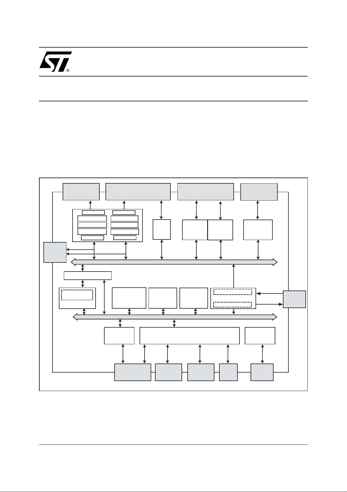
Figure 1. uPSD3234A Block Diagram
Dedicated
Pins (80-
pin pkg
only)
Port 3, UART,
Intr, Timers
8032 Core
2 UARTs
Interrupts
Port 0
DATA
PSD MCU Interface
PSD Page
Register
Decode PLD
Port 1, Bit I/O and I2C,
2nd UART and ADC
Port 1Port 3
4 ADCs
3 Timer/Cntrs
256B SRAM
Port 2
ADDR
128K or 256K
Main Flash
Byte
I2C
Master /
Slave
8032 Internal Bus
32K Byte
Secondary
Flash
PSD Internal Bus
CPLD - 16 MACROCELLSJTAG ISP
Port 4, PWM and DDC Port
PWM
4 Channels
8K Byte
SRAM
DDC
w/ 256 Byte
SRAM
Low Vcc Detect
Reset Supervisor
Watchdog Timer
Dedicated USB
Transceiver
8032 reset
PSD Reset
Pins
USB 1.1
&
Reset Input
Reset Output
VCC, GND,
XTAL
Dedicated
Pins
uPSD3200
Port C,
JTAG, PLD I/O
and GPIO
Port A, PLD
I/O and
GPIO
Port B, PLD
I/O and
GPIO
Port D
GPIO
Dedicated
Pins
AI06868b
1/49February 2005
Page 2

AN1560
TABLE OF CONTENTS
Figure 1. uPSD3234A Block Diagram. . . . . . . . . . . . . . . . . . . . . . . . . . . . . . . . . . . . . . . . . . . . . . . . 1
uPSD3200 FAMILY OVERVIEW. . . . . . . . . . . . . . . . . . . . . . . . . . . . . . . . . . . . . . . . . . . . . . . . . . . . . . . 4
DK3200 OVERVIEW . . . . . . . . . . . . . . . . . . . . . . . . . . . . . . . . . . . . . . . . . . . . . . . . . . . . . . . . . . . . . . . . 5
Figure 2. DK3200 Development Board. . . . . . . . . . . . . . . . . . . . . . . . . . . . . . . . . . . . . . . . . . . . . . . 5
DESIGN EXAMPLE BLOCK DIAGRAM. . . . . . . . . . . . . . . . . . . . . . . . . . . . . . . . . . . . . . . . . . . . . . . . . 6
Figure 3. Design Block Diagram . . . . . . . . . . . . . . . . . . . . . . . . . . . . . . . . . . . . . . . . . . . . . . . . . . . . 6
Figure 4. 8032 Memory Map. . . . . . . . . . . . . . . . . . . . . . . . . . . . . . . . . . . . . . . . . . . . . . . . . . . . . . . 7
ENTERING DESIGN IN PSDSOFT EXPRESS. . . . . . . . . . . . . . . . . . . . . . . . . . . . . . . . . . . . . . . . . . . . 9
Invoke PSDsoft Express and Create Project . . . . . . . . . . . . . . . . . . . . . . . . . . . . . . . . . . . . . . . . 9
Select MCU and Initial Placement of Flash in Code Space or Data Space. . . . . . . . . . . . . . . . . 9
Pin Definitions . . . . . . . . . . . . . . . . . . . . . . . . . . . . . . . . . . . . . . . . . . . . . . . . . . . . . . . . . . . . . . . . . 9
Figure 5. MCU Selection. . . . . . . . . . . . . . . . . . . . . . . . . . . . . . . . . . . . . . . . . . . . . . . . . . . . . . . . . 10
Figure 6. Pin Definitions . . . . . . . . . . . . . . . . . . . . . . . . . . . . . . . . . . . . . . . . . . . . . . . . . . . . . . . . . 11
Memory Map. . . . . . . . . . . . . . . . . . . . . . . . . . . . . . . . . . . . . . . . . . . . . . . . . . . . . . . . . . . . . . . . . . 12
Page Register. . . . . . . . . . . . . . . . . . . . . . . . . . . . . . . . . . . . . . . . . . . . . . . . . . . . . . . . . . . . . . . . . 12
Figure 7. Page Register Definition . . . . . . . . . . . . . . . . . . . . . . . . . . . . . . . . . . . . . . . . . . . . . . . . . 12
Chip-Select Equations . . . . . . . . . . . . . . . . . . . . . . . . . . . . . . . . . . . . . . . . . . . . . . . . . . . . . . . . . 13
Figure 8. Chip-Select Definition for 8K byte SRAM . . . . . . . . . . . . . . . . . . . . . . . . . . . . . . . . . . . . 13
Figure 9. Chip-Select Definition for Flash Memory Segments . . . . . . . . . . . . . . . . . . . . . . . . . . . . 14
Figure 10.External Chip-Select Definition for LCD Module . . . . . . . . . . . . . . . . . . . . . . . . . . . . . . . 15
I/O Logic Equations. . . . . . . . . . . . . . . . . . . . . . . . . . . . . . . . . . . . . . . . . . . . . . . . . . . . . . . . . . . . 15
Figure 11.Logic Equation for signal LCD_rw. . . . . . . . . . . . . . . . . . . . . . . . . . . . . . . . . . . . . . . . . . 16
User-Defined Node Equations . . . . . . . . . . . . . . . . . . . . . . . . . . . . . . . . . . . . . . . . . . . . . . . . . . .16
Figure 12.4-bit Down-Counter with Automatic Reload of Initial Count . . . . . . . . . . . . . . . . . . . . . . 16
Figure 13.D-register Node. . . . . . . . . . . . . . . . . . . . . . . . . . . . . . . . . . . . . . . . . . . . . . . . . . . . . . . . 17
Edit ABEL HDL Statements for PLD Design . . . . . . . . . . . . . . . . . . . . . . . . . . . . . . . . . . . . . . . . 17
Figure 14.Design Flow Diagram . . . . . . . . . . . . . . . . . . . . . . . . . . . . . . . . . . . . . . . . . . . . . . . . . . . 18
Additional µPSD Configuration . . . . . . . . . . . . . . . . . . . . . . . . . . . . . . . . . . . . . . . . . . . . . . . . . .20
C Code Generation . . . . . . . . . . . . . . . . . . . . . . . . . . . . . . . . . . . . . . . . . . . . . . . . . . . . . . . . . . . . 20
Figure 15.Coded Example Generation . . . . . . . . . . . . . . . . . . . . . . . . . . . . . . . . . . . . . . . . . . . . . . 20
Fitting Design. . . . . . . . . . . . . . . . . . . . . . . . . . . . . . . . . . . . . . . . . . . . . . . . . . . . . . . . . . . . . . . . . 20
Merging 8032 Firmware with µPSD Configuration . . . . . . . . . . . . . . . . . . . . . . . . . . . . . . . . . . . 21
Figure 16.Firmware Merging Utility . . . . . . . . . . . . . . . . . . . . . . . . . . . . . . . . . . . . . . . . . . . . . . . . . 22
Figure 17.Merging the Example Firmware . . . . . . . . . . . . . . . . . . . . . . . . . . . . . . . . . . . . . . . . . . . 23
JTAG Programming. . . . . . . . . . . . . . . . . . . . . . . . . . . . . . . . . . . . . . . . . . . . . . . . . . . . . . . . . . . . 23
Figure 18.Programming with FlashLINK JTAG Cable. . . . . . . . . . . . . . . . . . . . . . . . . . . . . . . . . . . 24
WATCH IT RUN ON DK3200 . . . . . . . . . . . . . . . . . . . . . . . . . . . . . . . . . . . . . . . . . . . . . . . . . . . . . . . . 25
USING UVISION2 AND ISD51 DEBUGGER FROM KEIL SOFTWARE, INC.. . . . . . . . . . . . . . . . . . . 26
Loading a Keil uVision2 Project. . . . . . . . . . . . . . . . . . . . . . . . . . . . . . . . . . . . . . . . . . . . . . . . . . 26
2/49
Page 3

AN1560
Building the Project and Programming the µPSD . . . . . . . . . . . . . . . . . . . . . . . . . . . . . . . . . . . 26
Running the Keil ISD51 UART Debugger . . . . . . . . . . . . . . . . . . . . . . . . . . . . . . . . . . . . . . . . . . 26
Figure 19.Debug icon . . . . . . . . . . . . . . . . . . . . . . . . . . . . . . . . . . . . . . . . . . . . . . . . . . . . . . . . . . . 26
Figure 20.Keil ISD51 Just After it is Successfully Invoked . . . . . . . . . . . . . . . . . . . . . . . . . . . . . . . 27
CONCLUSION. . . . . . . . . . . . . . . . . . . . . . . . . . . . . . . . . . . . . . . . . . . . . . . . . . . . . . . . . . . . . . . . . . . . 28
APPENDIX A.PSDSOFT EXPRESS PROJECT SUMMARY FILE, DK3200_1.SUM. . . . . . . . . . . . . . 29
APPENDIX B.PSDSOFT EXPRESS ABEL HDL FILE DK3200_1.ABL . . . . . . . . . . . . . . . . . . . . . . . 32
APPENDIX C.PSDSOFT EXPRESS FITTER REPORT DK3200_1.FRP . . . . . . . . . . . . . . . . . . . . . . . 36
APPENDIX D.DK3200 BOARD LAYOUT. . . . . . . . . . . . . . . . . . . . . . . . . . . . . . . . . . . . . . . . . . . . . . . 42
Figure 21.DK3200 Board Layout. . . . . . . . . . . . . . . . . . . . . . . . . . . . . . . . . . . . . . . . . . . . . . . . . . .42
APPENDIX E.DK3200 SCHEMATICS . . . . . . . . . . . . . . . . . . . . . . . . . . . . . . . . . . . . . . . . . . . . . . . . . 43
Figure 22.DK3200 Schematics (1) . . . . . . . . . . . . . . . . . . . . . . . . . . . . . . . . . . . . . . . . . . . . . . . . .43
Figure 23.DK3200 Schematics (2) . . . . . . . . . . . . . . . . . . . . . . . . . . . . . . . . . . . . . . . . . . . . . . . . .44
Figure 24.DK3200 Schematics (3) . . . . . . . . . . . . . . . . . . . . . . . . . . . . . . . . . . . . . . . . . . . . . . . . .45
Figure 25.DK3200 Schematics (4) . . . . . . . . . . . . . . . . . . . . . . . . . . . . . . . . . . . . . . . . . . . . . . . . .46
Figure 26.DK3200 Schematics (5) . . . . . . . . . . . . . . . . . . . . . . . . . . . . . . . . . . . . . . . . . . . . . . . . .47
REVISION HISTORY. . . . . . . . . . . . . . . . . . . . . . . . . . . . . . . . . . . . . . . . . . . . . . . . . . . . . . . . . . . . . . . 48
3/49
Page 4

AN1560
UPSD3200 FAMILY OVERVIEW
The uPSD3200 family is a standard 12-c lock per instruc tion 8032 MCU cap able of being cloc ked up to
40MHz at 5.0V and 24MHz at 3.3V at industrial oper ating temp erature ran ge. Currently ther e are seven
family members that are different comb inations of Flash memor y size, ope rating vo ltage, peri pheral set,
and packaging (see datash eet). The fullest featured pa rt, uPSD3234A-40U6, is used in this Applicati on
Note. The term µP SD i s us ed th ro ugh out the r e mai nde r of th e do cument for brevity. Se e µPSD block diagram in Figure 1..
The µPSD has a unique memory structure that includes two independent Flash memory arrays (main and
secondary) capab le of r ead-w hile-wr ite op eration. This is ideal for In-A ppli cation Pro grammin g (IA P) be cause the 8032 can fetch instructions from one Flash memory array while erasing/writing the other array.
Individual sectors of ea ch Flas h memory ar ray can be m apped to vi rtually an y 8032 addr ess by the De code PLD (DPLD) for total flexi bility. The µPSD al so contains a Page Register whose outputs feed the
inputs of the DPLD. This allows paging (or banking) of Flash memory to break the 8032’s inherent limit of
64K byte addresses. The 8032 may write to the Page Register at runtime.
For more complex designs, the µPSD is capable of placing each of the Flash memory arrays (Main or Secondary) into 8032 code address space, into 8032 data space, or into both code and data space on the fly.
Mapping flexibil ity li ke this supports IAP b ecause either Fl ash mem ory array may b e tempor arily pl aced
into data space while the firmware is updated, then moved back into code space when finished, all under
control of the 8032.
Many peripherals are ava ilable in this µ PS D, incl uding: USB v1.1 (lo w speed), two UART ch annels , four
PWM channels, one I
and projectors), a watch dog timer, low-V
GPIO.
All of the peripherals on Ports 1, 3, and 4 are controlled using 8032 Special Function Registers (SFRs). I/
O Signals on ports A, B, C , and D are controlled one of two ways: One, by a block of xdata memory
mapped control regis ters, whose b ase add ress (
by the programmable logic.
The JTAG ISP channel on Por t C is ideal for rapid code iterations during fir mware develo pment and for
Just-In-Time inventory management during manufacturing. JTAG ISP eliminates the need for sockets and
pre-programmed devices, and requi r es no partic i pati on of the 8032.
2
C channel, four 8-bit ADC channels, DDC (Data Display Channel for LCD monitors
detection with reset-ou t, a general purp ose PLD, and man y
CC
csiop
) can be mapped anywh ere usi ng the DPL D; Two,
4/49
Page 5
AN1560
DK3200 OVERVIEW
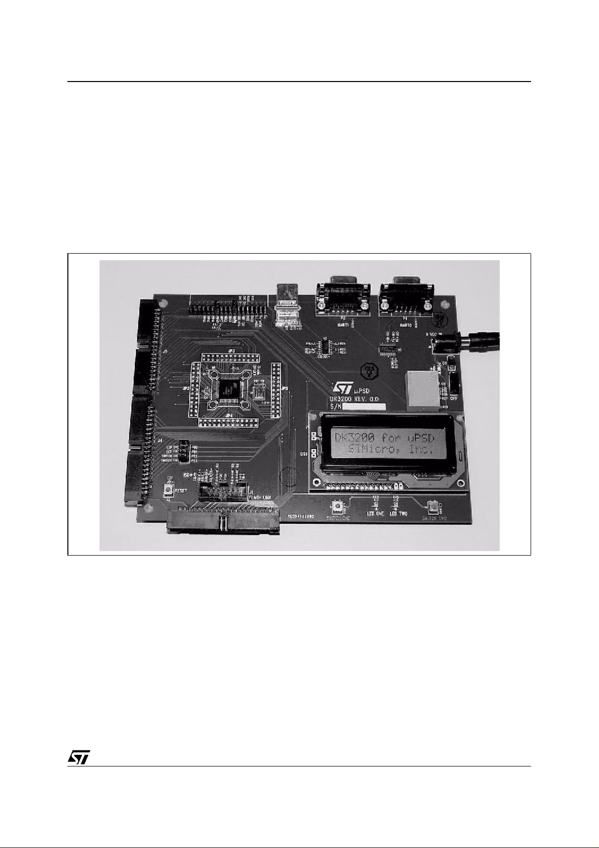
A picture of the DK320 0 board is shown in Figure 2.. Board layout and schematic s are in the Appen dix.
Connectors JP1, J3, J4, J5 provide easy access to all µPSD I/O signals for expansion or testing. JP1 accepts jumper shunts to wrap µ PSD ou tputs b ack into µ PSD i nputs f or tes ting. J 3, J4, J5 ca n conn ect directly to standard Agilent (HP) Logic analyzer pods. UARTs are available on P1 and P2. A USB host can
connect to the µPSD as a peri phe ral v ia J 2. The F lash LINK JTAG IS P cabl e co nnec ts at J1 . Conn ec tor s
JP2, JP3, JP4, JP5 allow direct connection of the In-Circuit Emulator from Nohau Corp, EMULuPSD3200-PC. JP6 ac cepts jumper s to c onnec t the sw itch es (SW 1, SW2) and the LEDs (LED 1, LED2)
to PSD port B. LED D5 indicates JTAG ISP Programming . The DK3200 also has a 2-line 16 character
LCD interface and a full featured real-time clock with SNAPHAT snap-on battery/crystal pack.
Figure 2. DK3200 Development Board
5/49
Page 6
AN1560
DESIGN EXAMPLE BLOCK DIAGRAM
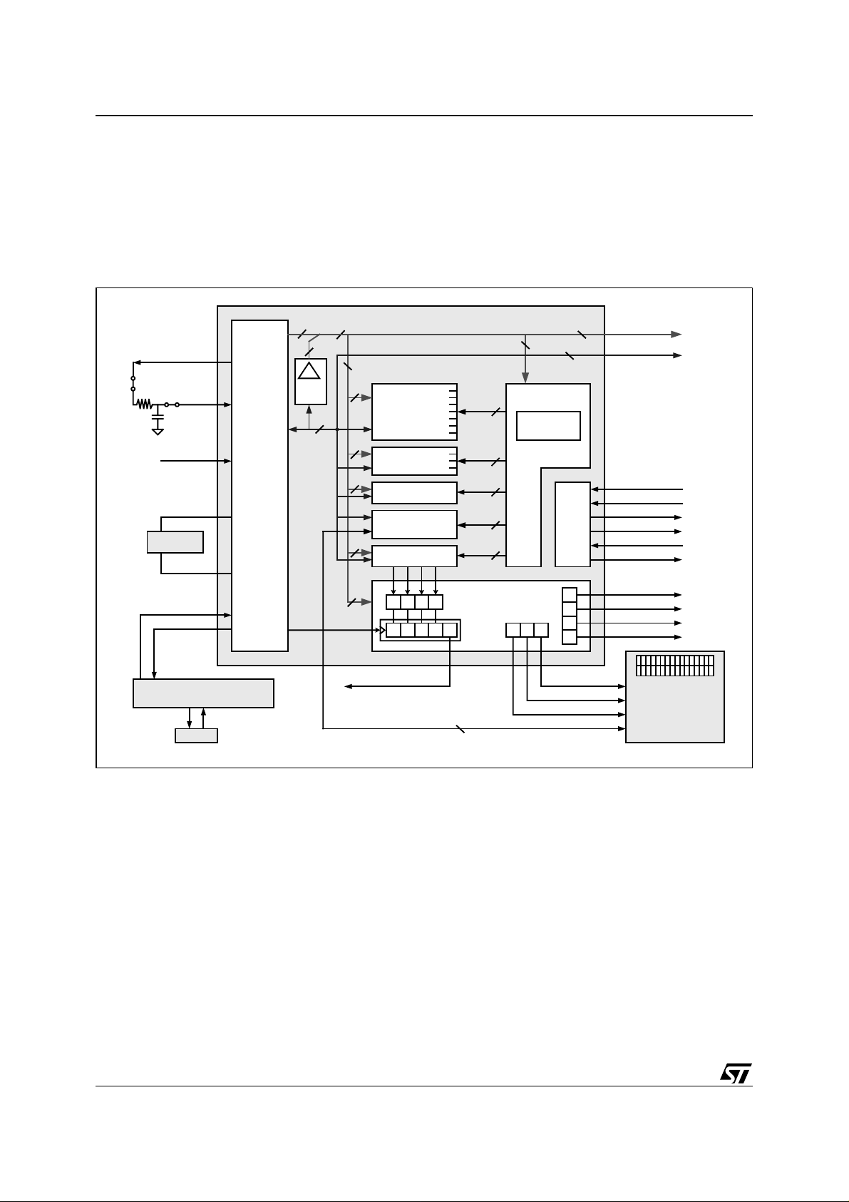
This simple design example is represented by the block diagram of Figure 3., and the memory map of
Figure 4.. All 16 macrocells of the PLD are used, Flash memory is paged, and few of the 8032 interfaces
(ADC, PWM, UART) are configured and used. The idea is to touch several aspects of the µPSD that may
be unfamiliar to a typica l 8051 user an d to give yo u an idea of how to use the des ign tools and be come
familiar with µPSD architecture.
Figure 3. Design Block Diagram
pin P4.7 (PMW0)
pin P1.4
(ADC0)
pin _RESET
pin XTAL1
40 MHz
pin XTAL2
pin P3.0 (RxD1)
pin P3.1 (TxD1)
RS-232 Transceiver
P1
A8 - A15
PWM0
ADC0
AD0-AD7
_RESET_IN
8032
XTAL1
XTAL2
RxD1
TxD1
Latch
ALE
8
8
DATA
ADDR
16
8
uPSD3234A-40U6
16
ADDR
15
256KB Main
Flash (data)
13
32KB 2ndary
Flash (code)
13
8KB SRAM
Data Bus
Repeater
8
256 Control Regs
16
pin PB4 (term_count)
16
fs0 - fs7
8
csboot0 -
csboot3
4
rs0
1
psel0 -
psel1
2
csiop
1
Initial Count
DownCounter
8
16 PLD
MarcoCells
pins PA0 - PA7 (LDC_d0 - LCD_d7)
ADDR
12
DATA pins P0.0 - P0.7
8
DPLD
Page Reg
(from Control
Regs)
JTAG
ISP
pin PB5 (LCD_rs)
pin PB6 (LCD_rw)
pin PB7 (LCD_e)
pins A0 - A11
pin PC0 (tms)
pin PC1 (tck)
pin PC3 (tstat)
pin PC4 (_terr)
pin PC5 (tdi)
pin PC6 (tdo)
pin PB0 (a12_x)
pin PB1 (a13_x)
pin PB2 (a14_x)
pin PB3 (a15_x)
REG SELECT
READ/WRITE
CHIP SELECT
D0 - D7
LCD
MODULE
AI07073
Figure 3. show s the de sign i mplem ented i n this appl ication note. Maj or el ements ar e the µ PS D, an LCD
module, and an RS-232 transceiver chip.
The 8032 outputs a repetitive PWM pulse train with a slowly varying pulse width to an RC network which
converts the pulse train in to a slowly sw eeping DC voltag e (0 to 5V). Th is DC signal i s looped back i nto
an ADC input. The 8032 will write the resulting Hexadecimal ADC conversion value to the LCD so you can
watch the results. The RC network and loop-back is implemented with two jumpers on the DK3200 board.
Additionally and independently, a 4-bit auto-reloading down-counter is created using PLD macrocells. The
8032 directly loads the initial count value into four macrocells, and that count is automatically loaded into
another four macrocells that create the 4-bit down-counter. Reloading occurs each time the counter reaches terminal count of zer o. Terminal count is indica ted externally by a puls e on a µPSD output pi n. The
down-counter is clocked by ALE signal (ALE was random choice, could be any signal). The 8032 may load
a different initial count at anytime, creating a variable divider of the ALE signal.
6/49
Page 7
AN1560
Four more macrocells a re us ed to outp ut the high four 8032 address sign als . T he 80-pi n µPSD only outputs the low twelve 8032 address signals on dedicated pins. If more address signals are needed externally, they have to be added this way using the PLD.
The LCD module is connected to the µPSD via a Port A for data and Port B for some glue logic and a chipselect signal. Port A is operating is an special data bus repeater mode this example, called Peripheral I/O
mode. 8032 data will pass through port A onl y for a given address range specifie d in PSDsoft Express
(illustrated later).
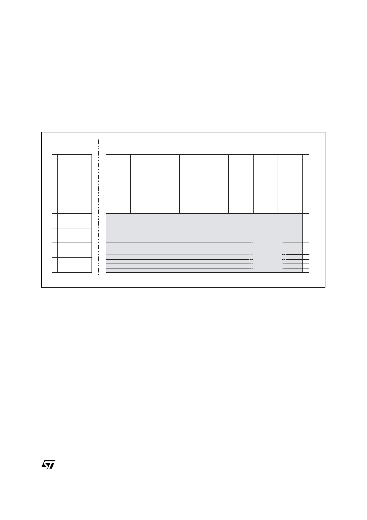
Figure 4. 8032 Memory Map
Code Space (_PSEN) Data Space (_RD and _WR)
FFFF
Page X Page 0
Page 3
Page 7Page 5 Page 6Page 4Page 2Page 1
FFFF
8000
7FFF
6000
5FFF
4000
3FFF
2000
1FFF
0000
nothing mapped
csboot3
8K bytes uPSD
Secondary Flash
csboot2
8K bytes uPSD
Secondary Flash
csboot1
8K bytes uPSD
Secondary Flash
csboot0
8K bytes uPSD
Secondary Flash
fs0
32K bytes uPSD
Main Flash
(xdata)
fs1
32K bytes uPSD
Main Flash
(xdata)
fs2
32K bytes uPSD
Main Flash
(xdata)
LCD_e and psel
32K bytes uPSD
Main Flash
(xdata)
nothing mapped
fs4
fs3
32K bytes uPSD
Main Flash
(xdata)
nothing mapped
, 8K bytes PSD SRAM (xdata)
rs0
chip select and data bus repeater for LCD module
csiop
, cntl regs for ports A, B, C, D (xdata)
fs5
32K bytes uPSD
Main Flash
(xdata)
fs6
32K bytes uPSD
Main Flash
(xdata)
Common
Memory
Across All
Data Pages
fs7
32K bytes uPSD
Main Flash
(xdata)
8000
7FFF
4000
2000 - 3FFF
0400 - 1FFF
0300 - 03FF
0200 - 02FF
0000 - 00FF
AI07074b
The memory map in Figure 4. shows th at th e 32K b yte sec ondary F lash me mory is used for 8032 co de,
and the 256K byte main Flash memory is used for 8032 data, banked over eight pages. The nomenclature
fsx, csbootx, rs0, csiop,
µPSD main Flash mem or y h as a total of e igh t 32K by te s egm ents (
memory has a total o f fo ur 8K byt e s eg men ts (
segment (
rs0
). A group of µ PS D co ntr ol regi st er s wh ic h c ont rol I/O ports A, B, C, and D li e i n a 2 56-by te
xdata address space whose base address is named
is enabled over a giv en address range as specified by
select signal,
LCD_e
and
psel
in Figure 4. refer to the individual internal µPSD memory segments. The
csboot0-csboot3
csiop
. The µPSD has a data bus repeater feature that
psel
. Figure 4. also shows one e xternal mem ory
fs0..fs7
). The µPSD 8K byte SRAM has a single
). The µPS D se condary Flash
, for the LCD module. This memory map is specified using the software tool PSDsoft
Express. Each memory segment can be placed at virtually any address, which provides an infinite number
of mapping schemes. This is just one example.
We’ll keep things simple for this particular application note, meaning the 8032 will “boot” and run code contained completely withi n the 32K byte seconda ry Flash memory i n code space and we’ll tr eat the 256K
byte main Flash me mory as data only. However, this memory map may grow with the need s of your
project. For example, if a large Flash memory is needed for code space and IAP is required, a slight variation of the map in Figure 4. can accomplish this. The 8032 can boot from secondary Flash memory (secondary Flash memory resides in code space from 0-7FFF as in Figure 4.), then the 8032 can calculate a
checksum on the main Flash memory and then program the main Flash memory if necessary (main Flash
memory resides in data space from 8000- FFFF on eight pa ges as in Figure4.). After the contents of main
7/49
Page 8

AN1560
Flash memory are verified, the 8032 c an write to s pecial register , called the VM regi ster within th e
register block, to “reclassify” the main Flash memory from data space to code space. After which, the 8032
will have access to 256K bytes of Flash memory for code in code space, paged across eight code pages
in upper memory (8000-FFFF), and the 8032 will have access to 32K bytes of Flash memory for code in
code space common to all pages in lower memory (0-7FFF). At that point no Flash memory will reside in
data space. Upon reset, the memory map is reset to look like Figure 4. again. The VM register can be accessed by the 8032 at runtime to perform a variety of manipulations. PSDsoft is used to set the initial value
of the VM register upon power-up. Future Application notes will illustrate various memory schemes.
csiop
8/49
Page 9

AN1560
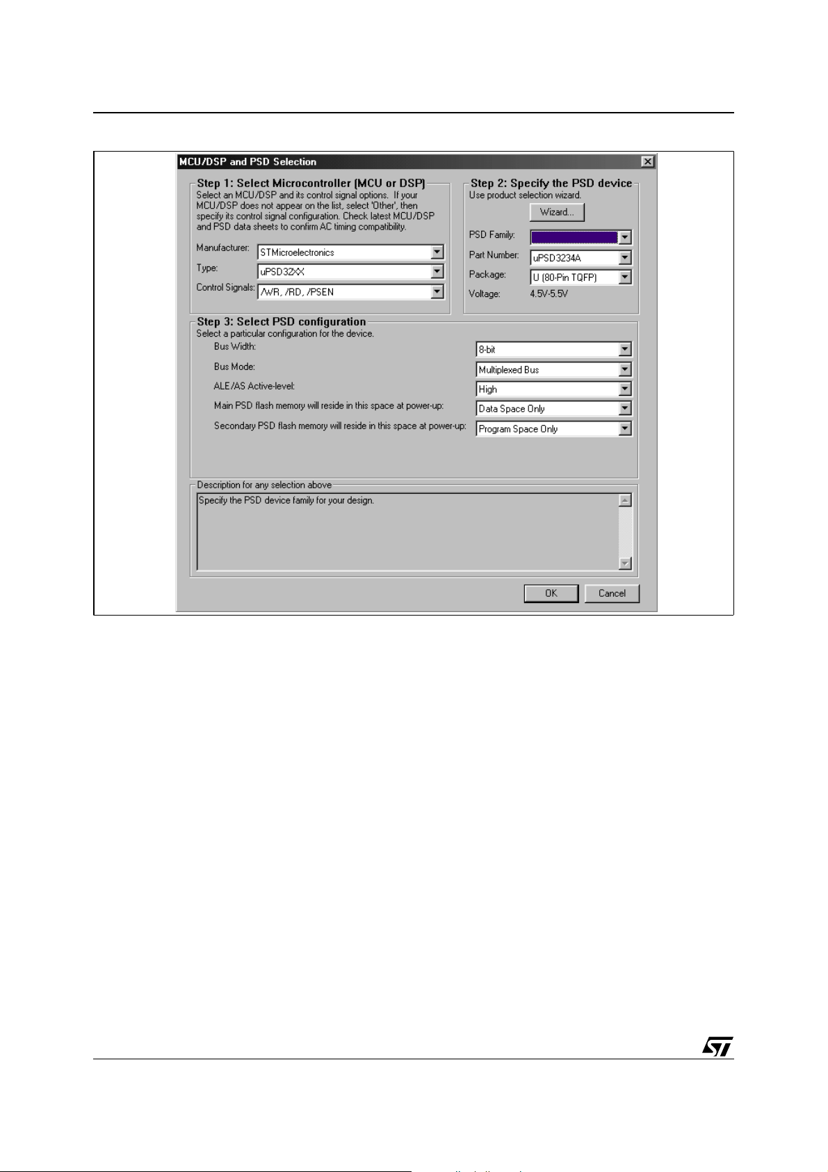
ENTERING DESIGN IN PSDSOFT EXPRESS
Highlights of the design process will be given here. The steps are simple and navigation through PSDsoft
Express is easy. Invoke PSDsoft Express and follow along if you wish. PSDsoft Express is included in the
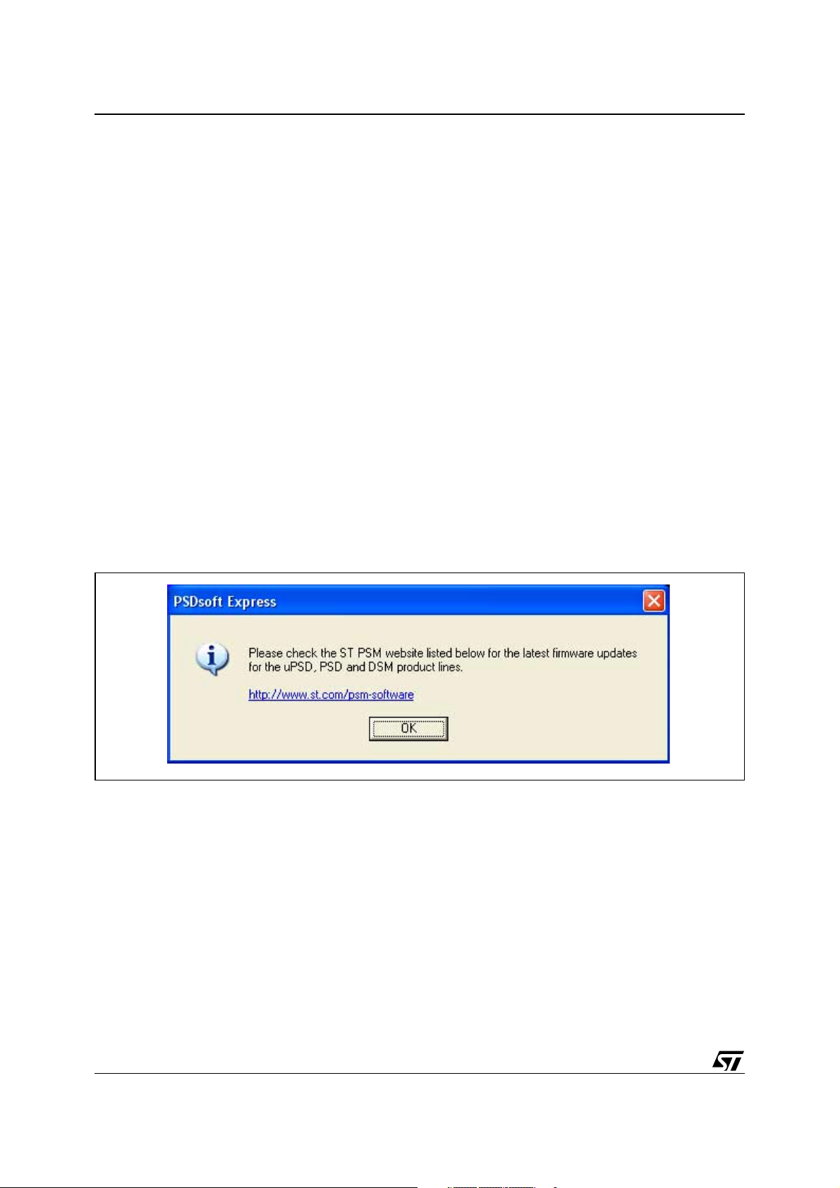
DK3200 CD, but you should check for latest updates. Updates are available from our web site at
www.st.com/psm, in the “Software Downloads” area.
Invoke PSDsoft Express and Create Project
■ Install PDSsoft Express (from the web or the included CD)
■ Start PSDsoft Express
■ Create a new project
■ Select your project folder and name the project (in this example, name the project “DK3200_1” in the
folder
PSDexpress\my_project\dk3200_dsn_1\
Note that the folder,
dk3200_dsn_1 under PSDexpress\my_project
ed.
Select MCU and Initial Placement of Flash in Code Space or Data Space
■ Select an MCU. In this case it is STMicroelectronics, then uPSD32xx, then uPSD3234A.
■ Select the main Flash memory to reside in 8032 data space at power-up (means that the 8032 _RD
and _WR signals are routed to the main Flash memory array)
■ Select the secondary Flash memory to reside in 8032 code space at power-up (means that the 8032
_PSEN signal is routed to the secondary Flash memory array)
Note: At runtime, the 8032 can alter the initial settings of code and data space by writing to the VM register.
Figure 5. shows what the screen should look like after you’ve made the selections.
Click OK. Now you will be asked i f you want to use the Desi gn Assis tant, Ex tended Design As sist ant, or
Example Template. Choose Example Template. This is a predefined design that matches this application
note and it runs on the DK3200 board. Next choose the template for the DK3200 Kit when prompted.
Pin Definitions
You will see the Pin Definitions screen appear. All of the pin definitions shown in block diagram of Figure 3.
are filled in. Click through the pins and see how they are configured and how they relate to Figure 3.. You’ll
notice that you cannot change the definition of some pins because they have a fixed function.
A comment about JTAG pins. Th is example us es 6-pin JTA G which is up to 30% fas ter than the defau lt
standard 4-pin JTAG. The two extra pins in the 6-pin JTAG configuration are
Now click “Next” to move on to the Design A ssistant fo r memory mapp ing and logic equations. You will
see the Page Register definition screen.
..
, does not exist and needs to be creat-
_tstat
and
terr
.
9/49
Page 10
AN1560
uPSD3000
Figure 5. MCU Selection
10/49
Page 11
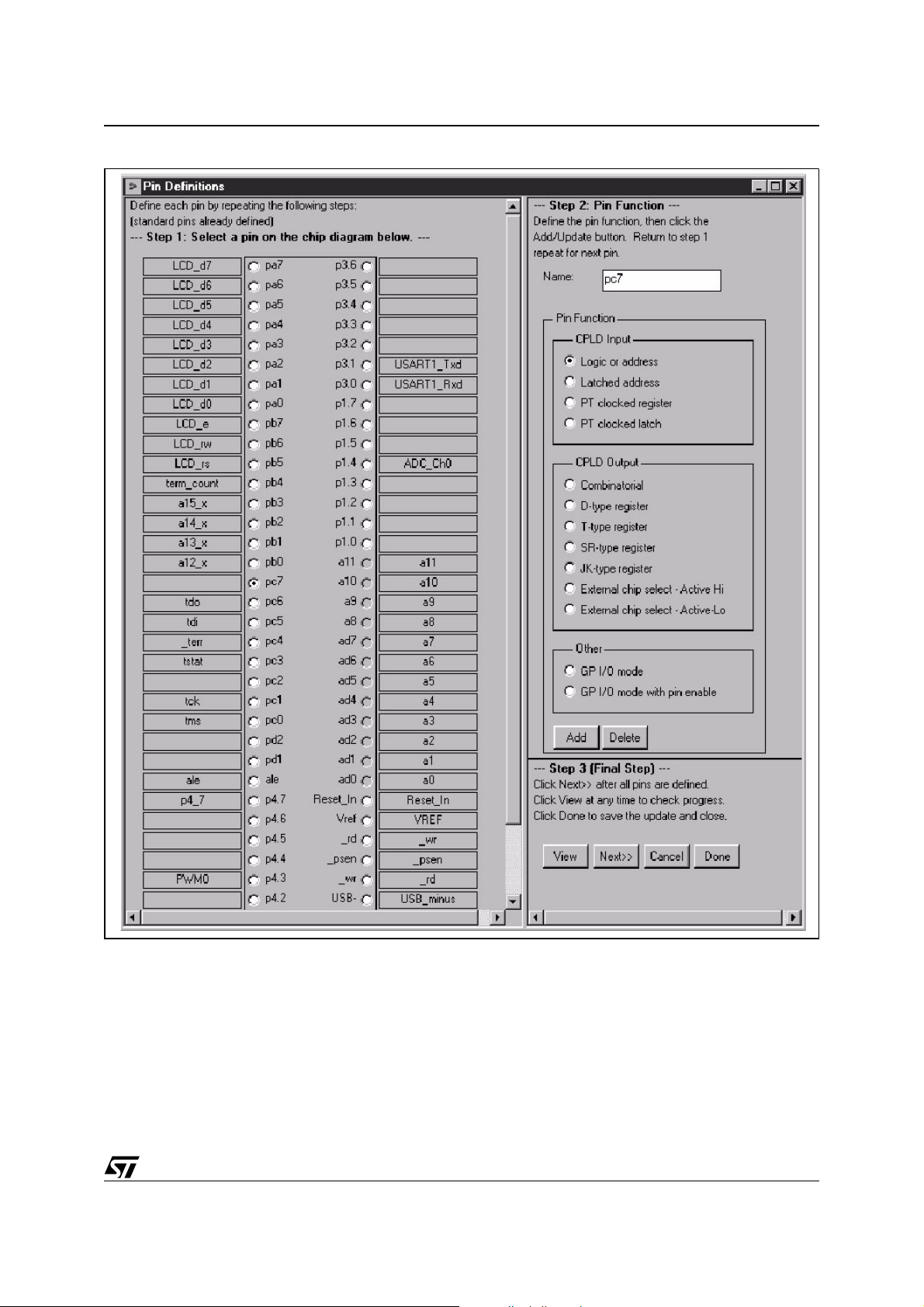
Figure 6. Pin Definitions
AN1560
11/49
Page 12
AN1560
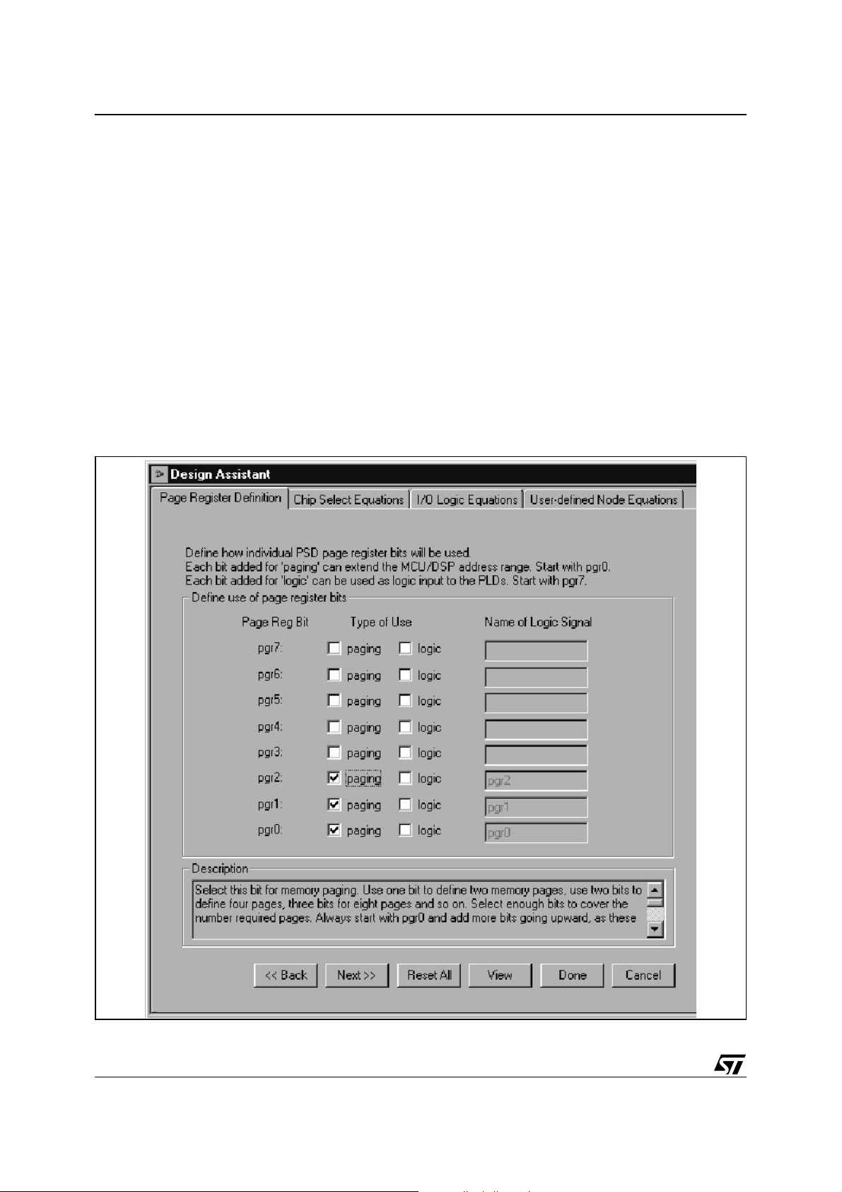
Memory Map
Defining the memory map requ ires defi ning the ad dress r ange of chip- sele cts for indiv idual me mory ele ments of the µPSD (memor y ex terna l to the 8032 c ore) . Defin ition of the use of the µPSD Page Regi ste r
is also required.
Four memory blocks (main Flash memory, secondary Flash memory, SRAM, and control registers) external to the 8032 core are available and are individually selected segment-by-segment when 8032 addresses are presented to the D ecode PLD (DPLD). E ach of these m emory segments ha s its own chip-se lect
name (
fs3, csboot1, rs0, c siop
must be specified using PSDsoft Express. For this example, chip-selects are defined to match the memory
map of Figure 4..
Page Register
Since eight memory pa ges (or banks) are ne eded as shown in Figure 4., thr ee paging bits (2
specified as sh ow n in Figure 7.. The µPSD supports up to 4 paging bits (pg0, pg1, pg2, pg3) for a total of
16 pages. Unused paging bits including pg4, pg5, pg6 and pg7 may be used for other functions. Note that
the paging bits used must be the LSB bits in the paging register. Click “Next”.
Figure 7. Page Register Definition
, etc.). Equations for these chip-s elect s, and fo r any e xternal chip-s elect s,
3
= 8) are
12/49
Page 13
AN1560
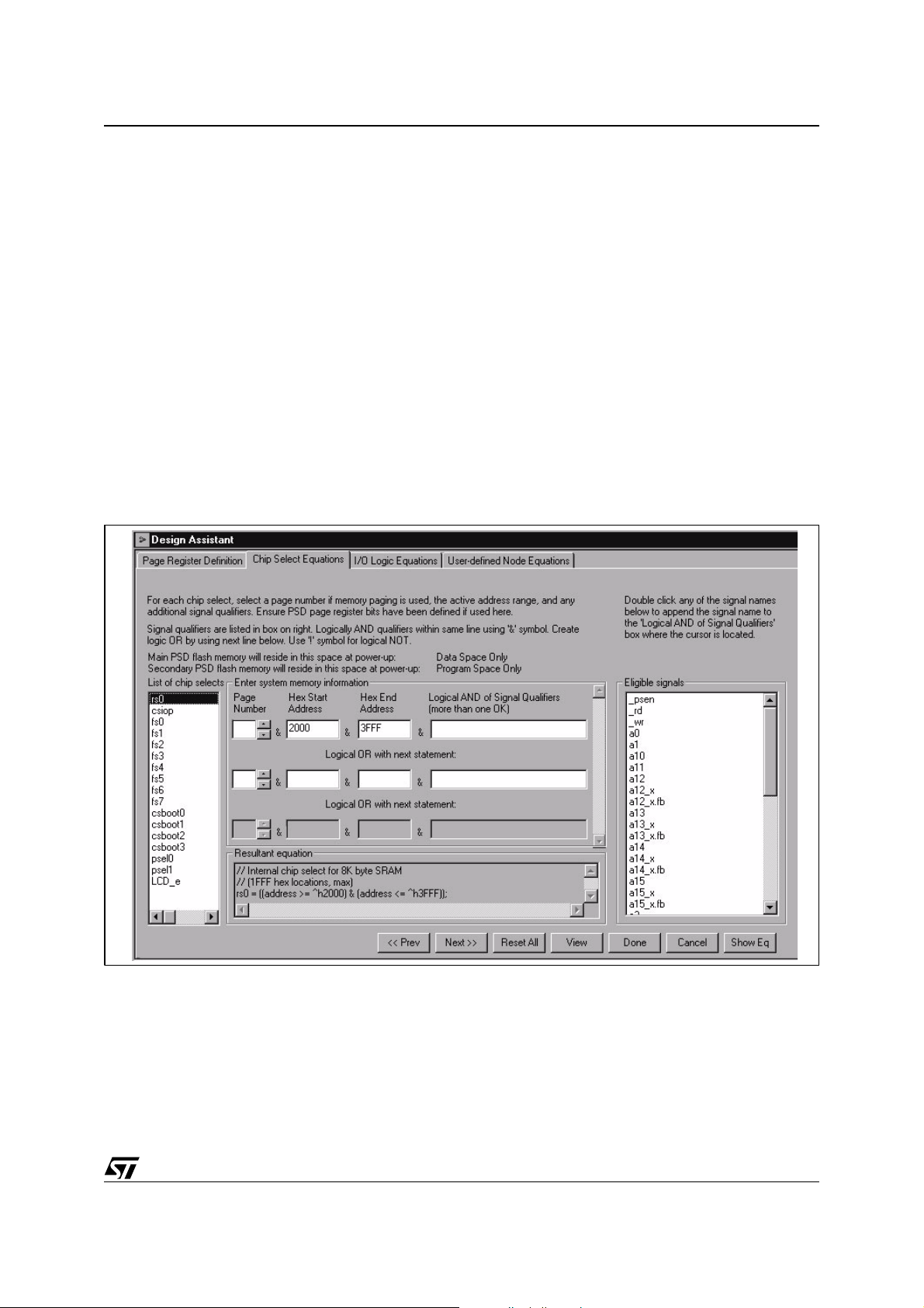
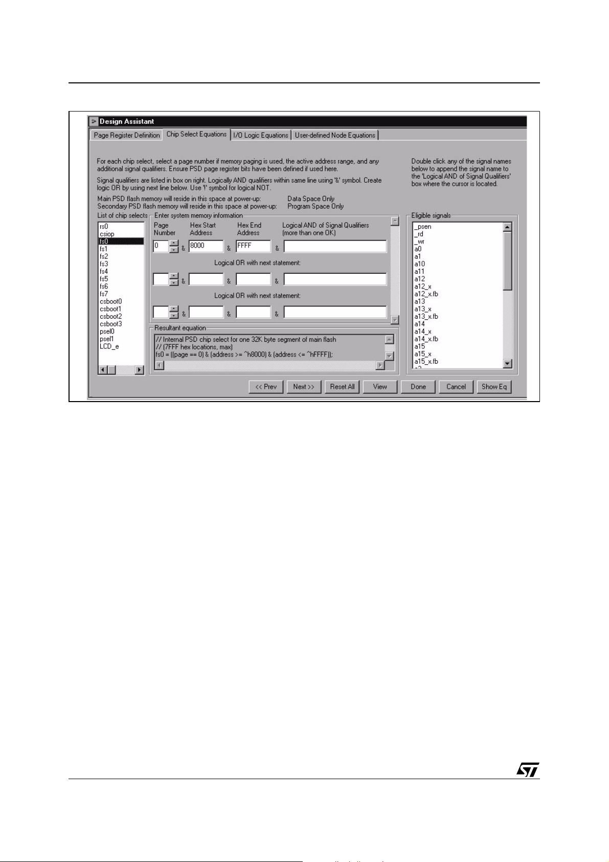
Chip-Select Equations
rs0
Now you will see the Chip- Sele ct de finition scr een. Clic k the chip- select signa l
SRAM, and see that its definition matches the memory map of Figure 4..
rs0
Notice that no page n umber is spe cified f or
dent). Additional signal qualifiers (8032 control signals
µPSD chip-selects as this is taken care of in silicon. The SRAM always defaults to 8032 data space.
At any time, you can click the “View” button to see how you are doing. A summary will appear.
csiop
Now click on the chip-select
control µPSD ports A, B, C, D, the Page Register, power management, and other functions. 40 of the 256
registers are used, se e µPSD datasheet for r egister definitions and th eir address offset from th e
base address. There i s no need to specify additional signal qu alifiers for
place
csiop
on a particular memory page. The
Next click on
Notice the page nu mbe r i s 0 for
Figure 4.. Cl ick on remain ing chip-selects f or main Flash m emory and notice the page number assign-
ments. No additional signal qualifiers are needed.
Figure 8. Chip-Select Definition for 8K byte SRAM
fs0. fs0 .. fs7
are chip-selects for the eight 32K byte segments of µPSD main Flash memory.
(Chip Select I/O Por t). This is a band o f 256 xdata registe rs used to
fs0
, and the address range is 8000 - FFFF as shown in memory map of
since the SRAM is c ommon to all pages (page i ndepen -
_rd, _wr, _psen, ale
) are NOT needed for internal
csiop
csiop
must be xdata address space.
for the 8K byte xdata
csiop
, and it is not allowed to
13/49
Page 14
AN1560
Figure 9. Chip-Select Definition for Flash Memory Segments
Now click on
ary Flash memory. Check the address assignments for each of these chip-selects and notice there are no
page numbers assigned. The secondary Flash memory is common to all pages.
Next click on
Peripheral I/O Mode to dr i ve the LCD m odule. Port A pins were ear lier sp ec ified a “Peripheral I/O M ode ”
which acts like a ‘245 bus tr ansceiver chi p connecting the 8032 d ata bus to exter nal peripher als over a
given address range specified by the label
trolled automatically in silicon by the 8032
have to do is click on
range as shown in Figure 4., with no Page Number assignment.
eral I/O feature is active for the logical OR of
And finally, clic k on
chip-select, we mus t include signal qualifiers
when the 8032 presents an a ddres s in the r ang e of 3 00 to 3F F AND wh en e ithe r 8032 co ntr ol signal
is true, OR when 8032 cont rol sig nal
Figure 10.. Since both signals
are specified as qualifiers. Signal qualifiers may be added by setting the cursor where you want the signal
name to go, then just double click on the signal name in the list of eligible qualifiers.
Click “next” to move on to logic definitions.
csboot0. csboot0 .. csboot3
psel0
. This address range specifies when Port A pins will behave like a data bus repeater in
psel0
and enter the address range 300 to 3FF to enable this feature for that address
LCD_e
. This is an external chip-select for the LCD module. Since this is an external
_rd
and
are chip-selects for the four 8K byte segments of µPSD second-
psel0
or
psel1
. The direction of this transceiver function is con-
_rd
and
_wr
signals. See µPSD data sheet for details. So all we
psel1
is not needed because the Periph-
psel0
or
psel1
.
_rd
and
_wr.
In this design,
_wr
is true. To create this log ic, in format ion is entere d as shown in
_wr
are active low, the logical NOT operator (!) is used when they
LCD_e
is true (active hi) only
_rd
14/49
Page 15
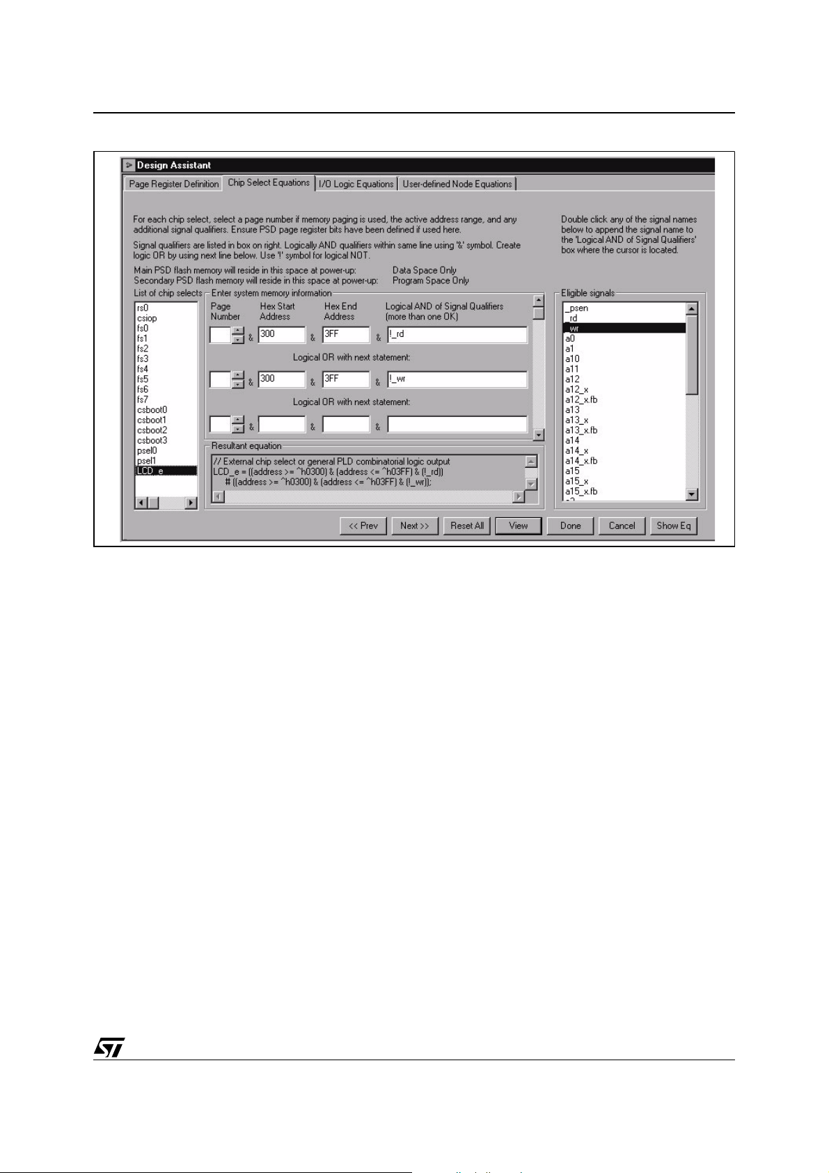
Figure 10. External Chip-Select Definition for LCD Module
AN1560
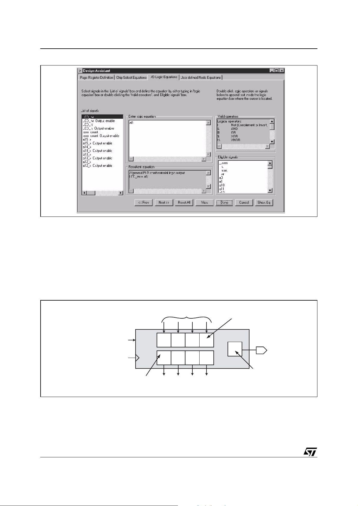
I/O Logic Equations
Defined here are equations for PLD outputs for the LCD interface signals, the additional 8032 address outputs, and the terminal count output signa l from the down-cou nter. The De sign Assista nt (DA) will c reate
HDL logic statements using the ABEL language in the background after you enter logic in this point-andclick design entry environment. The DA will also create all the declaration statements in ABEL. This saves
much typing and reduces the c han ce of err or . For m ore co mpl ic ate d lo gic PSDs oft al lo ws you to edit the
ABEL statements d irec tl y. In th is ex am pl e you’ ll s ee si mpl e l og ic entered point-and- clic k st yl e, a nd yo u’l l
see the 4-bit down-counter entered by editing the ABEL file directly.
Click on “
output signal “
logic operators are also available for general purpose logic.
LCD_rw
” as shown in Figure 11., and notice t hat the inter nal sign al a0 is assigned to drive the
LCD_rw
”. Although this was a very simple logic equation, AND, OR, XOR, NOT, and other
15/49
Page 16
AN1560
Figure 11. Logic Equation for signal LCD_rw
Click through the remaining signal names and observe the logic assigned. Notice there is no logic equation
assigned to
term_count
because that assignment will be mad e by editing the ABEL file directly. Click
“Next”.
User-Defined Node Equations
Here you will see how internal logic nodes are created. In this example there are four registers (or nodes)
to hold the initial count of t he 4-bit down- counter, and four additio nal registers to create th e actual 4 -bit
down-coun ter. See Figure 12..
Figure 12. 4-bit Down-Counter with Automatic Reload of Initial Count
4-bit auto-reloading
down-counter
8032 writes to OMCs in
control register space (csiop)
to load inital count
ALE
4 nodes to form
LOAD
counter
8032 data bus
(initial count)
D3D2D1D
AB0AB3 AB2 AB1
AB4AB7 AB6 AB5
QDQCQBQ
4 nodes to hold
0
A
initial count
term_count
1 PLD output
defined for
terminal count
AI07076
These nodes were crea ted by cl icking the “Def Node..” button, na ming the no de, and then selecti ng the
type node (combinato rial, D-register, J-K regi ster, etc.). In this example , all eight nodes are D-regi ster
type. When a regi ster is creat ed, you c an specify i t’s source of Input, C lock, Reset, as Set illu strated in
Figure 13..
16/49
Page 17
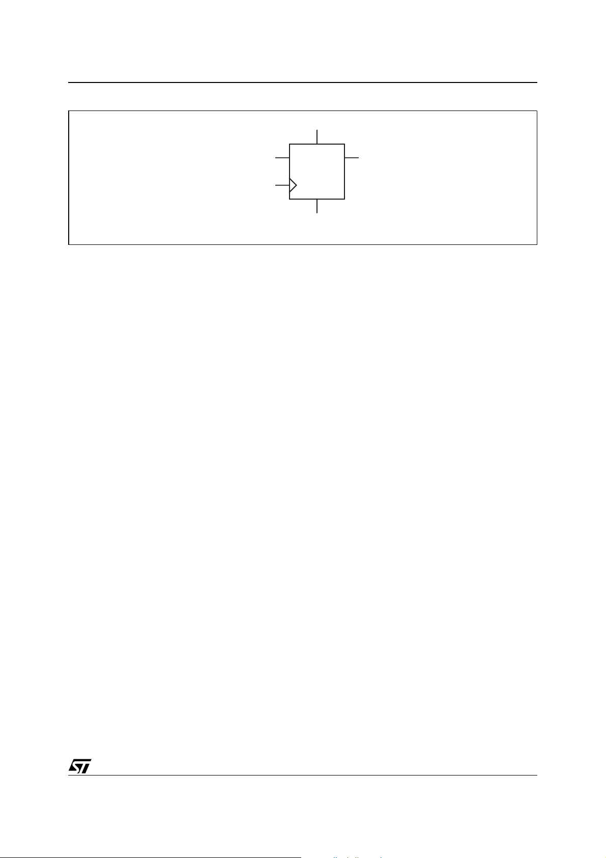
Figure 13. D-register Node
AN1560
Set
Input
Clock
PRE
CLR
Reset
QD
AI07077
Click though the sign al name s and loo k at the assign ments. Notice the re are n o defin itions fo r inp uts on
any of the eight nodes. For the
the
init_count
nodes, no log ic inpu t (or cl ock in put ) is s pecif ied becau se the 8032 will load the n odes di-
down_count
nodes, the inputs are defined elsewhere (the ABEL file). For
rectly by writing to the appropriate Output MacroCell register that resides the ban d of 256 registers of
csiop
.
It may seem odd to divide the design entry this way (some point-and-click entry and some direct ABLE file
editing), but many d eclarat ion s tatemen ts ar e auto maticall y cre ated i n the b ackgro und by th e p oint-and click entry. You wil l see that wh en it is time to e nter ABE L equations for the down-cou nter, ther e is very
little typing involved.
Click “Done”. Now you will see the m ain PS Dsoft flow di agram that wil l guide you throu gh the re maining
steps. You can see a summary report at this time by pulling down the “Report” selection in the main menu
bar at the top of the screen, then select “D esign Assista nt Summary ”. Your repo rt will match th e one in
Appendix A.
Edit ABEL HDL Statements for PLD Design
If your PSDsoft flow diagram does not include the block “Edit/Add Logic Statements” as shown in
Figure 14., then pull down the “Project” selection in the main menu bar at the top of the screen, then select
“Preference”. Click the box that says “Enable ABEL Editing Capability”, then “OK”.
17/49
Page 18

AN1560
Figure 14. Design Flow Diagram
Click the “Edit/Add Logic Statements” box. You will see an “HDL Assistant” window pop up. Browse
through this to see ABEL logic and syntax examples that you can cut and paste into future designs. Close
the HDL Assistant and you will see the ABEL HDL so urce file. All the declar ations and logic equat ions
generated from the Design Assistant are there, and should match Appendix B.
There are only two regions in the ABEL file in which you can type statements, otherwise the DA will overwrite what you have typed next time you get into the DA.
The first safe region is for ABEL dec larations and lies between the two st atements: “// Begin user preserved declarations” and “// End user preserved declarations”.
18/49
Page 19

AN1560
The second safe regio n is for logic equa tions and lies betwee n the two statements: “// Begin user pre served equations” and “// End user preserved equations”.
Scroll down to the declaration region in the ABEL file, it should look like:
// Begin user preserved declarations (not affected by iterations of DA usage) ===================
WSIPSD PROPERTY 'DataBus_OMC D[7:4]:down_count[3:0] MCELLAB'; // This statement forces the alignment
// of down_count bits [3..0] to the MCU data bus bit positions [7..4].
// If this WSIPSD PROPERTY statement was not present, then PSDsoft
// would pick random MCU bit positions. The WSIPSD PROPERTY is needed
// only if the MCU will read or write to MicroCells and only if a
// particular MCU data bus position is required by the designer.
WSIPSD PROPERTY 'DataBus_OMC D[3:0]:init_count[3:0] MCELLAB'; // This statement forces the alignment
// of init_count bits [3..0] to the MCU data bus bit positions [3..0].
DCOUNT = [down_count3..down_count0]; // 4-bit down counter
INIT = [init_count3..init_count0];// 4-bit initial count from MCU
//INIT = [0,1,0,0];
// End user preserved declarations (not affected by iterations of DA usage) ===================
Notice the WSIPSD PROPERTY statements. These are needed whenever you want to dictate the placement of certain mac rocel ls o f the PLD. If you do no t ente r any WS IPSD PROPERT Y d eclara tions state ment, then the PSDsoft “fitter” process will place the macrocells in random order. This is not a problem for
most designs. But in this example we want to load an initial count for the down-counter from the 8032 data
bus so we must ma ke s ur e the ou tpu t macrocells holding the initial co unt ar e in the c or rec t b it or der a nd
the correct position in the bank of eight output macrocells. The property statement:
WSIPSD PROPERTY ‘DataBus_OMC D[7:4]:down_count[3:0] MCELLAB’
forces the order of the bits of the down-counter and places them on the upper half of the 8032 data bus.
The property statement:
WSIPSD PROPERTY ‘DataBus_OMC D[3:0]:init_count[3:0] MCELLAB’
forces the order of the bits of the initial count and places them on the lower half of the 8032 data bus. Now
when the 8032 writes to the O MCAB regi ster at addr ess csiop +20h, the l ow four bits o f the byte wi ll get
loaded into the initia l count. There i s also a OMCAB mask registe r at csiop+22h that is used to prevent
the 8032 from disturbing the other bits in the OMCAB register while writing.
If the PROPERTY statements above ended with MCELLBC instead of MCELLAB, then the other bank of
eight output macrocells wo uld be used for the c ounter. See the µ PSD data sh eet and PSDsoft Express
User’s Guide for more details.
The next declaration statements DCOUNT and INIT create a shorthand notation for use in the logic equations.
Now scroll down in the ABEL file to the logic equations until you see:
// Begin user preserved equations (not affected by iterations of DA usage) ===================
term_count = (DCOUNT == 0); // term_count true when count reaches zero
when term_count then DCOUNT := INIT; // automatically reload counter with initial
// value after a count of zero is reached
else DCOUNT := DCOUNT - 1; // specify down count action
// End user preserved equations (not affected by iterations of DA usage) ===================
19/49
Page 20
AN1560
These three statements define the down-counter and the PLD output that appears on pin PB4
(term_count).
So you can see that very little typing is needed to im plement log ic desig ns. The sam e approach is used
to create state machines, shifters, etc.
Close the ABEL file and you will see the PSDsoft flow diagram again.
Additional µPSD Configuration
Click the box “Additional PS D Confi gur at ion ”. This is where yo u c an c hoos e to set the security bit to prevent a device prog rammer from ex amini ng or co pying the c ontents of th e µ PSD. The only way to def eat
the security bit is to erase the entire µPSD, then it can be u sed again as a blank pa rt. Yo u c an als o cl ic k
through the other s he ets o n this screen to set the J T AG USE RCO DE v al ue and s et sec tor p rotec ti on on
individual µPSD Non-Volatile memory segments. Just click “OK” for now.
C Code Generation
Clicking on the "Generate C Code" box pops up the message shown in Figure 15., directing you to the ST
web site where the example code can be downloaded. Click on the web site link (
software
From this web page in the "DK3200 - Software" section, download the "
dk32dsn1.zip
for this application note and it runs on the DK3 200 boa rd . It co n tai ns al l th e K eil s ourc e an d p ro ject fi le s
as well as all the PSD soft Express proj ect files. The PSDs oft Express proje ct files are not u sed in this
case since a new projec t is be ing cr ea ted b y fo ll owing this application note. The Keil sour ce and p ro je ct
files will be used later in this application note.
) in this window and it will launch the PC's web browser and direct it to the ST web page.
" file and unzip it to
C:\PSDexpress\my_project\dk3200_dsn_1
http:\\www.st.com\psm-
Example code file (1) -
. This is the comp let e pr ojec t
Figure 15. Coded Example Generation
In this screen you can specify a folder in which the ZIPPED project files will be written, along with a readme
file with instructi ons. The selecti on shown in Figure 15. is the complete project for this application note and
it runs on the DK3200 board. It contains all the Keil source and project files as well as all the PSDsoft Express project files. Now close the C Code Generation window.
Fitting Design
Click the next highl ig hted bo x i n the des ig n fl ow, “Fi t De si gn to S i lic on ”. PS Dsoft wil l co mpi le al l th e c on figuration selections and present a report (also available in Appendix C). The fitter report documents how
pins are configured and how the programmable logic is allocated. It also shows how many programmable
logic product terms are used, which is needed to estimate power consumption.
20/49
Page 21

AN1560
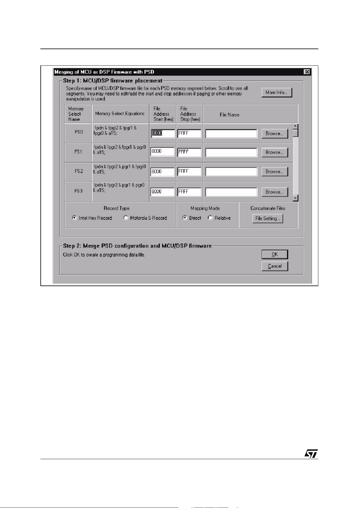
Merging 8032 Firmware with µPSD Configuration
Now that all µPSD pins and configuration settings have been defined, PSDsoft Express will create a single
object file (*.obj) that is a composite of the 8032 firmware (*.hex) and the µPSD configuration. FlashLINK
or third party progr ammer tools can u se thi s objec t fil e to pr ogram a µ PSD devic e. PS Dsoft Ex press will
create
During this merging process, PSDsoft Express will input firmware files from the 8032 compiler/linker in Srecord or Intel HEX format. It will map the content of these files into the physical memory segments of the
µPSD according to the ch oic es t hat were mad e in the ‘Ch ip Sele ct Eq uations’ screen. This mapp in g pro cess translates the absolute system addresses inside 8032 firmware files into physical internal µPSD addresses that are used by a programmer device to program the µPSD. This address translation process is
transparent. All you need to do is type (or browse) the fil e nam e that was gen er ated from the 803 2 lin ke r
into the appropriate boxes and PSDsoft Express does the rest. Y ou can specify a single file name for more
than one µPSD chip-select, or a different file name for each µPSD chip-select. It depends on how the 8032
linker has created the firmware file(s). For each µPSD chip-select in which you have specified a firmware
file name, PSDsoft Express will extract firmwa re from that file on ly between the spec ified start and stop
addresses, and ignore firmware outside of the start and stop addresses.
Click on 'Merge MCU Firm ware' in t he mai n flow dia gram. You will see an information wi ndow pop up to
remind you to be sur e y ou h av e confi gu re d the fi rm ware c om pil er and linker to suppo rt a paged memory
mapping scheme. “OK” and you'll see this screen:
DK3200_1.obj
for this design example.
21/49
Page 22
AN1560
Figure 16. Firmware Merging Utility
In the left column ar e µPSD memory segment chip-sele cts (FS 0, F S 1, etc. ). T h e n ex t c ol umn s how s the
logic equations for selection of e ach µPSD mem ory segment. These equations reflect the choices that
were made while defini ng µPSD internal chip-s elect equations in an earlier st ep. In the middle of the
screen are hexadeci mal start and stop addr esses that PS Dsoft Express h as filled in base d on the chip select equations. On the right are fields to enter (browse) the 8032 firmware files.
Select 'Intel Hex Record' for 'Record Type' as shown. Now slide the bar on the right side all the way down
to the bottom until you see CSBOOT0. Use the 'Browse' button and select the firmware file for CSBOOT0,
\PSDexpress\my_project\dk3200_dsn_1\dk3200_1_c\dk3200_1.hex
that exercises the PWM and ADC c hannels of t he µPS D on the DK320 0 board, and this code fits c ompletely within the 8K byte Flash memory segment CSBOOT0. The screen should look like this:
22/49
. This is a small example program
Page 23
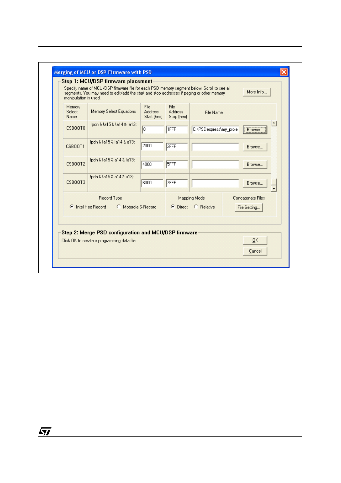
Figure 17. Merging the Example Firmware
AN1560
This specificatio n places firmw are in secon dary PS D Flash memor y segment csboo t0. PSDsoft Expres s
will extract any firmware that lies in side the file
and place it in PSD memory segment csboot0. Click OK to generate the composite object file,
DK3200_1.obj
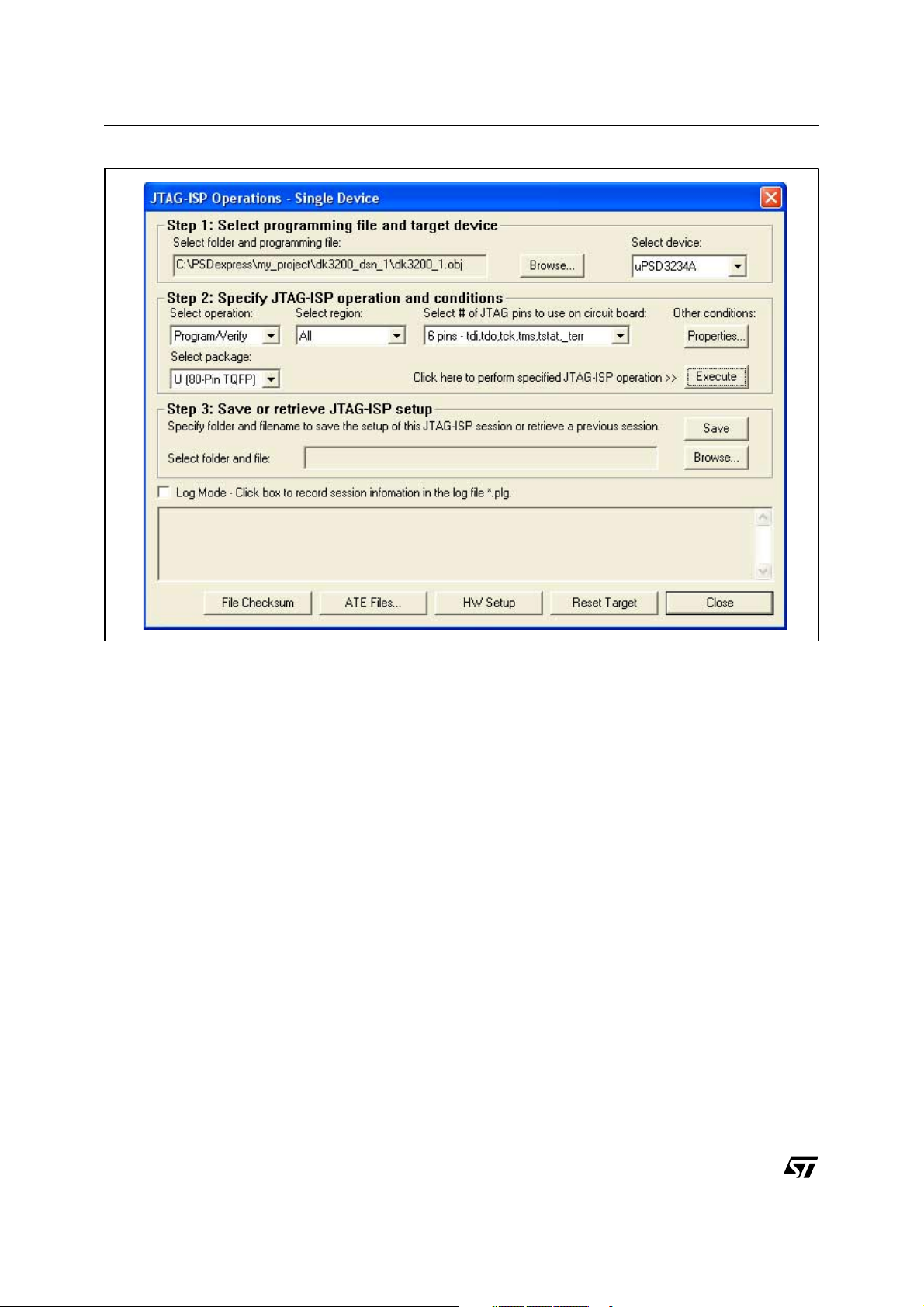
JTAG Programming
Now click the “STMicroelectronics JTAG/ISP” box to program the µPSD. You’ll be asked how many JTAG
devices are on the target circuit board, choose “Only One”. You’ll see the screen shown in Figure 18..
.
DK3200_1.hex
between MCU addresses 0000 and 1FFF
23/49
Page 24
AN1560
Figure 18. Programming with FlashLINK JTAG Cable
This window enables you to perform JTAG-ISP operations and also offers a loop back test for your
FlashLINK cable. If this is your first use, test your FlashLINK cable and PC parallel port by clicking the 'HW
Setup' button, then click 'LoopTest' button and follow the directions.
Now let's define our JTAG-ISP environment. For this example project, PSDsoft Express should have filled
in the folder and filename o f the obje ct file to progr am, the PSD devic e, and the JTAG-ISP operation, as
shown in the screen above. For this design example, we have chosen to use all six JT AG-ISP pins (instead
of four), so the screen should indicates 6-pin JTAG is being used.
To begin programming, connect the JTAG cable to the target sys tem, power-up the target syst em, and
click 'Execute' on the JTAG screen. The Log window at the bottom of the JTAG screen shows the progress.
Programming should just take a few seconds, the ISP LED at D5 on the DK3200 will light during programming.
There are optional choices available when the 'Properties.." button is clicked. One choice includes setting
the state of all pins on port A, B, C, or D during JTAG-ISP operations (make them inputs or outputs). The
default state of these pins is "input", which is fine for this design example. The other choice allows you to
specify a USERCODE value to compare before any JTAG-ISP operation starts. This is typically used in a
manufacturing environment (see on-screen description for details).
After JTAG-ISP operations are complete, you can save the JTAG setup for this programming session to a
file for later use. To do so, click on the 'Sav e' butt on. To restore the setup of a different previous sessi on,
click the 'Browse..' button.
24/49
Page 25

AN1560
WATCH IT RUN ON DK3200
After JTAG programming completes in just a few seconds, you should see a message appear on the LCD:
DK3200 for µPSD
PWM to ADC DEMO
Then you’ll see the Hexadecimal value of the ADC conversion sweep up and down between 00h and FFh
as the PWM pulse width changes. If you do not see the ADC value change, make sure there are two jumpers installed on the DK320 0 boa rd . On JP1, in sta ll one j ump er acr oss the two op pos i te rows of pin s ne xt
to the word “PWM0”, and the other jumper across the opposite rows of pins next to the word “ADC0”. Remove the jumper next the word “ADC0” and watch the ADC value on the LCD drop to 00h.
25/49
Page 26

AN1560
USING UVISION2 AND ISD51 DEBUGGER FROM KEIL SOFTWARE, INC.
This next section will briefly highlight the features of the Keil uVision2 IDE (Integrated Development Environment). Keil’s evaluation software was used for this example. This software is supplied on the DK3200
CD and can be ins talled by doubl e clicki ng on th e instal lation p rogram found in the Kei l subdire ctory. In
the case of version 7.20, the installation program is named
tation for more details.
Loading a Keil uVision2 Project
The file
source and proje ct f iles need ed to build this desig n in Keil’s uVision2. O nc e d ownl oa ded save the file on
your hard drive and unz ip it to the fo lder of your c hoice. The ZI P file contains two folders, DK 3200_1_c
and
for this application note.
Copy the folder
..
Now open the uVision2 project that you just got from the ZIP file at
.
.\keil\c51\DK3200_1_C\DK3200_1.uv2
Building the Project and Programming the µPSD
You can build the project for this application note which will create a new Intel HEX-80 file,
Invoke PSDsoft Express and open the project
this new HEX file at
merge, then program the DK3200 board with FlashLINK cable just as before. The LCD should display the
PWM/ADC demo information.
Running the Keil ISD51 UART Debugger
This simple demo program has the ISD51 UART debugger linked into the code. This is a new debug tool
from Keil that only consumes 700 bytes of code space and is royalty-free so it can stay in your end product
all the time. Unlike the older UART debugger, MON51, this debugger does not require you to debug code
in small sections a t a time f rom x data SRAM . And unlike M ON51, t his de bugger does not requi re yo u to
combine your code and data space (tie _PSEN and _RD together). See Keil documentation for details.
This proj ect,
rial COM1 port at 19.2 kbaud with no hardware handshaking. It also assumes there is a 40MHz crystal on
the DK3200 board. Connect a DB-9 (nine-pin) male-female straight-through (pins 2 and 3 are not
swapped) serial cable to COM1 port1 on your PC and to the UART0 (P1) connector on the DK3200 board.
Click the Debug icon shown in Figure 19., the debugger will start and it will compare contents of the Flash
memory in the µPSD Flash memory with the source files, then program execution will begin running to the
C source line until just after the function, ISD_check(), then it will stop and wait for your debug command.
The screen should look like Figure 20..
dk32dsn1.zip
DK3200_1_p. DK3200_1_c
\Keil\C51\DK3200_1_c
DK3200_1.Uv2
is available from the ST web site (
has all the Keil files,
DK3200_1_c
. Invoke Keil uVis io n2, p ul l down the “Project” menu, th en s elec t “ Op en Pr oje ct”.
and all of its contents to your Keil folders as follows,
. Everything should be ready to go.
DK3200_1
\keil\c51\DK3200_1_C\DK3200_1.hex
has ISD51 already selected for the debugger tool, connected through PC se-
EK51V720.exe
http:www.st.com/psm-software
DK3200_1_p
has the PSDsoft Express project files
. Please refer to Keil documen-
). It contains all the
DK3200_1.hex
, go to the “Merge MCU Firmware” section, select
for the Flash memory segment
csboot0
and
.
Figure 19. Debug icon
26/49
Page 27

Figure 20. Keil ISD51 Just After it is Successfully Invoked
AN1560
Now you can set breakpoints, single-step, view 8032 internal registers and SFRs, view blocks of memory,
etc. For example, in t he mem or y wind ow in the lower-right co rn er of the IDE scr een , th e by te of mem or y
at Hexadecimal addres s 96h is the SF R named “ADAT”, which is the resulting 8-bi t value fr om the ADC
channel from the last voltage co nversion before the 8032 stop ped. The value at address 96h is BF h in
Figure 20.. If y ou set a breakpoi nt on the functio n uPSD_ADC_Read( 0), then run the prog ram, you will
see the data byte at address 96h change value in the memory watch window, and that same data byte will
be showing on the LCD. Each t ime to run un til the br eakp oint, y ou sho uld s ee a ne w valu e appea ring in
the memory watch window at address 96h and the same value on the LCD. Click the debug icon again to
exit the debugger ISD51.
27/49
Page 28

AN1560
CONCLUSION
Congratulations! You have seen the majority of steps to implement a µPSD design on the DK3200 board.
Now you have a basis to understand more detail as you read the µPSD data sheet and the documentation
from Keil Software Inc.
28/49
Page 29

AN1560
APPENDIX A. PSDSOFT EXPRESS PROJECT SUMMARY FILE , DK3200_1.SUM
***********************************************************************
PSDsoft Express Version 8.30
Summary of Design Assistant
***********************************************************************
PROJECT : DK3200_1 DATE : 09/28/2004
DEVICE : uPSD3234A TIME : 16:35:05
MCU/DSP : uPSD32XX
***********************************************************************
Initial setting for Program and Data Space:
===========================================
Main PSD flash memory will reside in this space at power-up: Data Space Only
Secondary PSD flash memory will reside in this space at power-up: Program Space Only
Pin Definitions:
================
Pin Signal Pin
Name Name Type
------------ ------------------------- -----------pa7 LCD_d7 Peripheral I/O mode
pa6 LCD_d6 Peripheral I/O mode
pa5 LCD_d5 Peripheral I/O mode
pa4 LCD_d4 Peripheral I/O mode
pa3 LCD_d3 Peripheral I/O mode
pa2 LCD_d2 Peripheral I/O mode
pa1 LCD_d1 Peripheral I/O mode
pa0 LCD_d0 Peripheral I/O mode
pb7 LCD_e External chip select - Active Hi
pb6 LCD_rw Combinatorial
pb5 LCD_rs Combinatorial
pb4 term_count Combinatorial
pb3 a15_x Combinatorial
pb2 a14_x Combinatorial
pb1 a13_x Combinatorial
pb0 a12_x Combinatorial
tdo tdo Dedicated JTAG - TDO
tdi tdi Dedicated JTAG - TDI
pc4 _terr Dedicated JTAG - /TERR
pc3 tstat Dedicated JTAG - TSTAT
pc2 vstby SRAM standby voltage input
tck tck Dedicated JTAG - TCK
tms tms Dedicated JTAG - TMS
ale ale ALE output
p4.7 PWM4 GP I/O mode
p4.3 PWM0 PWM0 Output
p3.1 USART1_Txd UART1 TxD
p3.0 USART1_Rxd UART1 RxD
p1.4 ADC_Ch0 ADC channel0 input
a11 a11 Address line
a10 a10 Address line
a9 a9 Address line
a8 a8 Address line
ad7 a7 Data/Address line
ad6 a6 Data/Address line
ad5 a5 Data/Address line
ad4 a4 Data/Address line
29/49
Page 30

AN1560
ad3 a3 Data/Address line
ad2 a2 Data/Address line
ad1 a1 Data/Address line
ad0 a0 Data/Address line
_Reset_In Reset_In Reset In
Vref VREF VREF input
_rd _wr Bus control output
_psen _psen Bus control output
_wr _rd Bus control output
USB- USB_minus USB- bus
USB+ USB_plus USB+ bus
Xtal1 Xtal1 Xtal1
Xtal2 Xtal2 Xtal2
User defined nodes:
===================
Node Node
Name Type
------------ -----------down_count0 D-type register
down_count1 D-type register
down_count2 D-type register
down_count3 D-type register
init_count0 D-type register
init_count1 D-type register
init_count2 D-type register
init_count3 D-type register
Page Register settings:
=======================
pgr0 is used for paging
pgr1 is used for paging
pgr2 is used for paging
pgr3 is not used
pgr4 is not used
pgr5 is not used
pgr6 is not used
pgr7 is not used
Equations:
==========
rs0 = ((address >= ^h2000) & (address <= ^h3FFF));
csiop = ((address >= ^h0200) & (address <= ^h02FF));
fs0 = ((page == 0) & (address >= ^h8000) & (address <= ^hFFFF));
fs1 = ((page == 1) & (address >= ^h8000) & (address <= ^hFFFF));
fs2 = ((page == 2) & (address >= ^h8000) & (address <= ^hFFFF));
fs3 = ((page == 3) & (address >= ^h8000) & (address <= ^hFFFF));
fs4 = ((page == 4) & (address >= ^h8000) & (address <= ^hFFFF));
fs5 = ((page == 5) & (address >= ^h8000) & (address <= ^hFFFF));
fs6 = ((page == 6) & (address >= ^h8000) & (address <= ^hFFFF));
fs7 = ((page == 7) & (address >= ^h8000) & (address <= ^hFFFF));
csboot0 = ((address >= ^h0000) & (address <= ^h1FFF));
csboot1 = ((address >= ^h2000) & (address <= ^h3FFF));
csboot2 = ((address >= ^h4000) & (address <= ^h5FFF));
csboot3 = ((address >= ^h6000) & (address <= ^h7FFF));
psel0 = ((address >= ^h0300) & (address <= ^h03FF) & (_psen));
30/49
Page 31

LCD_e = ((address >= ^h0300) & (address <= ^h03FF) & (!_rd))
# ((address >= ^h0300) & (address <= ^h03FF) & (!_wr));
LCD_rw = a0;
LCD_rw.oe = Vcc;
LCD_rs = a1;
LCD_rs.oe = Vcc;
a15_x = a15;
a15_x.oe = Vcc;
a14_x = a14;
a14_x.oe = Vcc;
a13_x = a13;
a13_x.oe = Vcc;
a12_x = a12;
a12_x.oe = Vcc;
down_count0.ck = ale;
down_count0.re = !_reset;
down_count0.pr = Gnd;
down_count1.ck = ale;
down_count1.re = !_reset;
down_count1.pr = Gnd;
down_count2.ck = ale;
down_count2.re = !_reset;
down_count2.pr = Gnd;
down_count3.ck = ale;
down_count3.re = !_reset;
down_count3.pr = Gnd;
init_count0.ck = Gnd;
init_count0.re = !_reset;
init_count0.pr = Gnd ;
init_count1.ck = Gnd;
init_count1.re = !_reset;
init_count1.pr = Gnd;
init_count2.ck = Gnd;
init_count2.re = !_reset;
init_count2.pr = Gnd;
init_count3.ck = Gnd;
init_count3.re = !_reset;
init_count3.pr = Gnd;
AN1560
31/49
Page 32

AN1560
APPENDIX B. PSDSOFT EXPRESS ABEL HDL FILE DK3200_1.ABL
module DK3200_1
LCD_d7 PIN 21; “Reserved for Peripheral I/O mode
LCD_d6 PIN 22; “Reserved for Peripheral I/O mode
LCD_d5 PIN 24; “Reserved for Peripheral I/O mode
LCD_d4 PIN 26; “Reserved for Peripheral I/O mode
LCD_d3 PIN 28; “Reserved for Peripheral I/O mode
LCD_d2 PIN 32; “Reserved for Peripheral I/O mode
LCD_d1 PIN 34; “Reserved for Peripheral I/O mode
LCD_d0 PIN 35; “Reserved for Peripheral I/O mode
LCD_e PIN 66;
LCD_rw PIN 67;
LCD_rs PIN 72;
term_count PIN 73;
a15_x PIN 74;
a14_x PIN 76;
a13_x PIN 78;
a12_x PIN 80;
tdo PIN 6; “TDO
tdi PIN 7; “TDI
_terr PIN 9; “/TERR
tstat PIN 14; “TSTAT
vstby PIN 15; “SRAM standby voltage input
tck PIN 16; “TCK
tms PIN 20; “TMS
ale PIN 4; “ALE output
PWM4 PIN 18; “GP I/O
PWM0 PIN 27; “PWM0 Output
USART1_Txd PIN 77; “UART1 TxD
USART1_Rxd PIN 75; “UART1 RxD
ADC_Ch0 PIN 59; “ADC channel0 input
a11 PIN 57; “Address line
a10 PIN 55; “Address line
a9 PIN 53; “Address line
a8 PIN 51; “Address line
a7 PIN 47; “Data/address bus line
a6 PIN 45; “Data/address bus line
a5 PIN 43; “Data/address bus line
a4 PIN 41; “Data/address bus line
a3 PIN 39; “Data/address bus line
a2 PIN 38; “Data/address bus line
a1 PIN 37; “Data/address bus line
a0 PIN 36; “Data/address bus line
Reset_In PIN 68;
VREF PIN 70; “VREF input
_wr PIN 65;
_psen PIN 63;
_rd PIN 62;
USB_minus PIN 8; “USB- bus
USB_plus PIN 10; “USB+ bus
Xtal1 PIN 48; “Xtal1
Xtal2 PIN 49; “Xtal2
psel0 node;
rs0 node;
csiop node;
fs0 node;
fs1 node;
fs2 node;
fs3 node;
32/49
Page 33

fs4 node;
fs5 node;
fs6 node;
fs7 node;
csboot0 node;
csboot1 node;
csboot2 node;
csboot3 node;
_reset node 543;
a12 node 512;
a13 node 513;
a14 node 514;
a15 node 515;
pgr2..pgr0 node;
down_count0 NODE istype ‘reg_D’;
down_count1 NODE istype ‘reg_D’;
down_count2 NODE istype ‘reg_D’;
down_count3 NODE istype ‘reg_D’;
init_count0 NODE istype ‘reg_D’;
init_count1 NODE istype ‘reg_D’;
init_count2 NODE istype ‘reg_D’;
init_count3 NODE istype ‘reg_D’;
jtagsel node;
X = .x.;
address = [a15..a0];
page = [pgr2..pgr0];
Vcc = 1;
Gnd = 0;
AN1560
// Begin user preserved declarations (not affected by iterations of DA usage)
===================
WSIPSD PROPERTY ‘DataBus_OMC D[7:4]:down_count[3:0] MCELLAB’; // This statement forces the
alignment
// of down_count bits [3..0] to the MCU data bus bit positions
[7..4].
// If this WSIPSD PROPERTY statement was not present, then PSDsoft
// would pick random MCU bit positions. The WSIPSD PROPERTY is needed
// only if the MCU will read or write to MicroCells and only if a
// particular MCU data bus position is required by the designer.
WSIPSD PROPERTY ‘DataBus_OMC D[3:0]:init_count[3:0] MCELLAB’; // This statement forces the
alignment
// of init_count bits [3..0] to the MCU data bus bit positions [3..0].
DCOUNT = [down_count3..down_count0]; // 4-bit down counter
INIT = [init_count3..init_count0];// 4-bit initial count from MCU
//INIT = [0,1,0,0];
// End user preserved declarations (not affected by iterations of DA usage)
===================
equations
33/49
Page 34

AN1560
jtagsel = !_reset;
rs0 = ((address >= ^h2000) & (address <= ^h3FFF));
csiop = ((address >= ^h0200) & (address <= ^h02FF));
fs0 = ((page == 0) & (address >= ^h8000) & (address <= ^hFFFF));
fs1 = ((page == 1) & (address >= ^h8000) & (address <= ^hFFFF));
fs2 = ((page == 2) & (address >= ^h8000) & (address <= ^hFFFF));
fs3 = ((page == 3) & (address >= ^h8000) & (address <= ^hFFFF));
fs4 = ((page == 4) & (address >= ^h8000) & (address <= ^hFFFF));
fs5 = ((page == 5) & (address >= ^h8000) & (address <= ^hFFFF));
fs6 = ((page == 6) & (address >= ^h8000) & (address <= ^hFFFF));
fs7 = ((page == 7) & (address >= ^h8000) & (address <= ^hFFFF));
csboot0 = ((address >= ^h0000) & (address <= ^h1FFF));
csboot1 = ((address >= ^h2000) & (address <= ^h3FFF));
csboot2 = ((address >= ^h4000) & (address <= ^h5FFF));
csboot3 = ((address >= ^h6000) & (address <= ^h7FFF));
psel0 = ((address >= ^h0300) & (address <= ^h03FF) & (_psen));
LCD_e = ((address >= ^h0300) & (address <= ^h03FF) & (!_rd))
# ((address >= ^h0300) & (address <= ^h03FF) & (!_wr));
LCD_rw = a0;
LCD_rw.oe = Vcc;
LCD_rs = a1;
LCD_rs.oe = Vcc;
a15_x = a15;
a15_x.oe = Vcc;
a14_x = a14;
a14_x.oe = Vcc;
a13_x = a13;
a13_x.oe = Vcc;
a12_x = a12;
a12_x.oe = Vcc;
down_count0.ck = ale;
down_count0.re = !_reset;
down_count0.pr = Gnd;
down_count1.ck = ale;
down_count1.re = !_reset;
down_count1.pr = Gnd;
down_count2.ck = ale;
down_count2.re = !_reset;
down_count2.pr = Gnd;
down_count3.ck = ale;
down_count3.re = !_reset;
down_count3.pr = Gnd;
init_count0.ck = Gnd;
init_count0.re = !_reset;
init_count0.pr = Gnd ;
init_count1.ck = Gnd;
init_count1.re = !_reset;
init_count1.pr = Gnd;
init_count2.ck = Gnd;
init_count2.re = !_reset;
init_count2.pr = Gnd;
init_count3.ck = Gnd;
init_count3.re = !_reset;
init_count3.pr = Gnd;
// Begin user preserved equations (not affected by iterations of DA usage)
===================
34/49
Page 35

AN1560
term_count = (DCOUNT == 0); // term_count true when count reaches zero
when term_count then DCOUNT := INIT; // automatically reload counter with initial
// value after a count of zero is reached
else DCOUNT := DCOUNT - 1; // specify down count action
// End user preserved equations (not affected by iterations of DA usage)
===================
end DK3200_1
35/49
Page 36

AN1560
APPENDIX C. PSDSOFT EXPRESS FITTER REPORT DK3200_1.FRP
****************************************************************************************
**
PSDsoft Express Version 8.30
Output of PSD Fitter
****************************************************************************************
**
PROJECT : DK3200_1 DATE : 09/28/2004
DEVICE : uPSD3234A TIME : 16:33:47
FIT OPTION : Keep Current
DESCRIPTION: Example design for uPSD3234A in Application Note AN1560.
Simple memory map with 32K secondary flash in code space, and
256K main flash paged in data space. Down-Counter built in
PLD. Runs on DK3200 board.
****************************************************************************************
**
==== Pin Layout for U (80-Pin TQFP) Package Type ====
---------------------------- | |
|1 ] pd2 adio4 [41| Address Bus
a4/Data Port d4, ad4
|2 ] p3_3 p3_5 [42|
|3 ] pd1 adio5 [43| Address Bus
a5/Data Port d5, ad5
ale |4 ] pd0 p3_6 [44|
|5 ] pc7 adio6 [45| Address Bus
a6/Data Port d6, ad6
tdo, TDO |6 ] pc6/TDO p3_7 [46|
tdi, TDI |7 ] pc5/TDI adio7 [47| Address Bus
a7/Data Port d7, ad7
USB_minus |8 ] USBm Xtal1 [48| Xtal1
_terr, TERR |9 ] pc4/TERR Xtal2 [49| Xtal2
USB_plus |10] USBp VCC [50|
|11] N/C adio8 [51| Address Bus a8, a8
|12] VCC p1_0 [52|
|13] GND adio9 [53| Address Bus a9, a9
tstat, TSTAT |14] pc3/TSTAT p1_1 [54|
vstby |15] pc2 adio10 [55| Address Bus a10, a10
tck, TCK |16] pc1/TCK p1_2 [56|
|17] N/C adio11 [57| Address Bus a11, a11
PWM4 |18] p4_7 p1_3 [58|
|19] p4_6 p1_4 [59| ADC_Ch0
tms, TMS |20] pc0/TMS p1_5 [60|
LCD_d7 ,Peripheral I/O Mode |21] pa7 p1_6 [61|
LCD_d6 ,Peripheral I/O Mode |22] pa6 cntl0 [62| _rd
|23] p4_5 cntl2 [63| _psen
LCD_d5 ,Peripheral I/O Mode |24] pa5 p1_7 [64|
|25] p4_4 cntl1 [65| _wr
LCD_d4 ,Peripheral I/O Mode |26] pa4 pb7 [66| LCD_e
PWM0 |27] p4_3 pb6 [67| LCD_rw
LCD_d3 ,Peripheral I/O Mode |28] pa3 Reset_In [68| Reset_In
|29] GND GND [69|
|30] p4_2 Vref [70| VREF
|31] p4_1 N/C [71|
LCD_d2 ,Peripheral I/O Mode |32] pa2 pb5 [72| LCD_rs
|33] p4_0 pb4 [73| term_count
LCD_d1 ,Peripheral I/O Mode |34] pa1 pb3 [74| a15_x
36/49
Page 37

AN1560
LCD_d0 ,Peripheral I/O Mode |35] pa0 p3_0 [75| USART1_Rxd
ad0, Address Bus a0/Data Port d0 |36] adio0 pb2 [76| a14_x
ad1, Address Bus a1/Data Port d1 |37] adio1 p3_1 [77| USART1_Txd
ad2, Address Bus a2/Data Port d2 |38] adio2 pb1 [78| a13_x
ad3, Address Bus a3/Data Port d3 |39] adio3 p3_2 [79|
|40] p3_4 pb0 [80| a12_x
| |
---------------------------- ==== Global Configuration ====
Data Bus : 8-Bit
Address/Data Mode : Multiplexed
ALE/AS Signal : Active High
Control Signals : /WR, /RD, /PSEN
Main PSD flash memory will reside in this space at power-up : Data space
Secondary PSD flash memory will reside in this space at power-up : Program space
Enable Chip-Select Input(/CSI) : OFF
Standby Voltage Input (PC2) : ON
Standby-on Indicator (PC4) : OFF
RDY/Busy function (PC3) : OFF
Load Micro-Cell on : edge
Security Protection : OFF
==== DataBus_IMC access information ====
CSIOP
Location Address Offset Register Name Signals
--------------------------------------------------------
===== Resource Usage Summary =====
Total Product Terms Used: 72
Device Resources used / total
-----------------------------------------------Port A: (pins 35 34 32 28 26 24 22 21)
I/O Pins : 8 / 8
GP I/O or Address Out : 0
Peripheral I/O : 8
Logic Inputs : 0
Address Latch Inputs : 0
PT Dependent Latch Inputs : 0
PT Dependent Register Inputs : 0
Combinatorial Outputs : 0
Registered Outputs : 0
Other Information
Microcells : 8 / 8
Micro-Cells AB :
Buried Microcells : 8
Output Microcells : 0
Product Terms : 15 / 24
Control Product Terms : 24 / 34
Port B: (pins 80 78 76 74 73 72 67 66)
I/O Pins : 8 / 8
GP I/O or Address Out : 0
Logic Inputs : 0
Address Latch Inputs : 0
PT Dependent Latch Inputs : 0
37/49
Page 38

AN1560
PT Dependent Register Inputs : 0
Combinatorial Outputs : 8
Registered Outputs : 0
Other Information
Microcells : 8 / 8
Micro-Cells AB :
Buried Microcells : 0
Output Microcells : 0
Micro-Cells BC :
Buried Microcells : 0
Output Microcells : 8
Product Terms : 9 / 32
Control Product Terms : 8 / 34
Port C: (pins 20 16 15 14 9 7 6 5)
I/O Pins : 7 / 8
GP I/O or Address Out : 0
Logic Inputs : 0
Address Latch Inputs : 0
PT Dependent Latch Inputs : 0
PT Dependent Register Inputs : 0
JTAG signals : 6
Standby Voltage Input : 1
Rdy/Bsy signal : 0
Standby On Indicator : 0
Combinatorial Outputs : 0
Registered Outputs : 0
Other Information
Microcells : 8 / 8
Micro-Cells BC :
Buried Microcells : 8
Output Microcells : 0
Product Terms : 9 / 32
Control Product Terms : 0 / 34
Port D: (pins 4 3 1)
I/O Pins : 1 / 3
GP I/O or Address Out : 0
Logic Inputs : 0
Chip-Select Input : 0
Clock Input : 0
Control Signal Input : 1
Fast Decoding Outputs : 0
Other Information
Product Terms : 0 / 3
Control Product Terms : 0 / 3
==== OMC Resource Assignment ====
Resources PT User
Used Allocation Name
--------------------------------------------------------Micro-Cell AB :
Micro-Cells 0 - init_count0 => Register
Micro-Cells 1 - init_count1 => Register
Micro-Cells 2 - init_count2 => Register
Micro-Cells 3 - init_count3 => Register
Micro-Cells 4 - down_count0 => Register
38/49
Page 39

Micro-Cells 5 - down_count1 => Register
Micro-Cells 6 - down_count2 => Register
Micro-Cells 7 - down_count3 => Register
Micro-Cell BC :
Micro-Cells 0 - a12_x (mcellbc0) => Combinatorial
Micro-Cells 1 - a13_x (mcellbc1) => Combinatorial
Micro-Cells 2 - a14_x (mcellbc2) => Combinatorial
Micro-Cells 3 - a15_x (mcellbc3) => Combinatorial
Micro-Cells 4 - term_count (mcellbc4) => Combinatorial
Micro-Cells 5 - LCD_rs (mcellbc5) => Combinatorial
Micro-Cells 6 - LCD_rw (mcellbc6) => Combinatorial
Micro-Cells 7 - LCD_e (mcellbc7) => Combinatorial
External Chip Select :
========= Equations =========
DPLD EQUATIONS :
=======================
fs0 = !pdn & !pgr2 & !pgr1 & !pgr0 & a15;
fs1 = !pdn & !pgr2 & !pgr1 & pgr0 & a15;
AN1560
fs2 = !pdn & !pgr2 & pgr1 & !pgr0 & a15;
fs3 = !pdn & !pgr2 & pgr1 & pgr0 & a15;
fs4 = !pdn & pgr2 & !pgr1 & !pgr0 & a15;
fs5 = !pdn & pgr2 & !pgr1 & pgr0 & a15;
fs6 = !pdn & pgr2 & pgr1 & !pgr0 & a15;
fs7 = !pdn & pgr2 & pgr1 & pgr0 & a15;
csboot0 = !pdn & !a15 & !a14 & !a13;
csboot1 = !pdn & !a15 & !a14 & a13;
csboot2 = !pdn & !a15 & a14 & !a13;
csboot3 = !pdn & !a15 & a14 & a13;
csiop = !pdn & !a15 & !a14 & !a13 & !a12 & !a11 & !a10 & a9 & !a8;
rs0 = !pdn & !a15 & !a14 & a13;
psel0 = !pdn & _psen & !a15 & !a14 & !a13 & !a12 & !a11 & !a10 & a9 & a8;
jtagsel = !_reset;
PORTA EQUATIONS :
=======================
init_count0.D := 0;
init_count0.PR = 0;
init_count0.RE = !_reset;
init_count0.C = 0;
39/49
Page 40

AN1560
init_count1.D := 0;
init_count1.PR = 0;
init_count1.RE = !_reset;
init_count1.C = 0;
init_count2.D := 0;
init_count2.PR = 0;
init_count2.RE = !_reset;
init_count2.C = 0;
init_count3.D := 0;
init_count3.PR = 0;
init_count3.RE = !_reset;
init_count3.C = 0;
down_count0.D := (!down_count0.Q & !term_count.PIN)
# (init_count0 & term_count.PIN);
down_count0.PR = 0;
down_count0.RE = !_reset;
down_count0.C = ale;
down_count1.D := (down_count1.Q & down_count0.Q & !term_count.PIN)
# (!down_count1.Q & !down_count0.Q & !term_count.PIN)
# (init_count1 & term_count.PIN);
down_count1.PR = 0;
down_count1.RE = !_reset;
down_count1.C = ale;
down_count2.T := (!down_count1.Q & !down_count0.Q & !term_count.PIN)
# (!down_count2.Q & init_count2 & term_count.PIN)
# (down_count2.Q & !init_count2 & term_count.PIN);
down_count2.PR = 0;
down_count2.RE = !_reset;
down_count2.C = ale;
down_count3.T := (!down_count3.Q & init_count3 & term_count.PIN)
# (down_count3.Q & !init_count3 & term_count.PIN)
# (!down_count2.Q & !down_count1.Q & !down_count0.Q & !term_count.PIN);
down_count3.PR = 0;
down_count3.RE = !_reset;
down_count3.C = ale;
PORTB EQUATIONS :
=======================
a12_x = a12;
a12_x.OE = 1;
a13_x = a13;
a13_x.OE = 1;
a14_x = a14;
a14_x.OE = 1;
a15_x = a15;
a15_x.OE = 1;
term_count = !down_count3.Q & !down_count2.Q & !down_count1.Q & !down_count0.Q;
term_count.OE = 1;
40/49
Page 41

term_count.LE = 1;
LCD_rs = a1;
LCD_rs.OE = 1;
LCD_rw = a0;
LCD_rw.OE = 1;
LCD_e = (!_rd & !a15 & !a14 & !a13 & !a12 & !a11 & !a10 & a9 & a8)
# (!_wr & !a15 & !a14 & !a13 & !a12 & !a11 & !a10 & a9 & a8);
LCD_e.OE = 1;
PORTC EQUATIONS :
=======================
PORTD EQUATIONS :
=======================
--- End ---
AN1560
41/49
Page 42

AN1560
APPENDIX D. DK3200 BOARD LAYOUT
Figure 21. DK3200 BOARD LAYOUT
1
42/49
Page 43

APPENDIX E. DK3200 SCHEMATICS
Figure 22. DK3200 SCHEMATICS (1)
ADDR[11..8]
RD_
ALE
PSEN_
E
AD[7..0]
WR_
DDC_SYNC
DDC_CLK
PWM[4..0]
I2C_DATA
DDC_DATA
I2C_CLK
AN1560
of
TXD
TXD1
PA[7..0]
PB[7..0]
ADC[3..0]
PD1
{Doc} A
DK3200 Eval Board
B
Title
Size Document Number Rev
15Monday, June 10, 2002
E
Date: Sheet
D
AD1
AD2
AD3
AD4
AD5
AD6
AD7
1
.01
C4
.01
C3
1
VCC_1
50
12
U1
C5
.01
AD0
3637383941434547515355
AD0/P0.0
VREF
70
CPU_CLK
R1
4
U7
R41
4.7K
C2
C1
VCC_1 VCC_1
C
B
VCC_1
C6
A
.01
AD1/P0.1
AD2/P0.2
VCC_2
VCC_1
48
100
3
VCC
OE
1
AD3/P0.3
AD4/P0.4
XTAL_1
OUT
AD5/P0.5
AD6/P0.6
AD7/P0.7
XTAL_2
49
GND
ADDR8
A8/P2.0
P3.2/INT0
79
2
CMX750PCCH
ADDR9
ADDR10
A9/P2.1
P3.3/INT1
2
ADDR11
57
A10/P2.2
A11/P2.3
P3.4/T0
40
656246863
RD/CTRL1
WR/CTRL0
T1/P3.5
42
ALE/PD0
PSEN/CTRL2
CNT2/P1.0
PWM0
PWM2
PWM1
PWM3
DDC_CLK
PWM4
272523191830313344
PWM0/P4.3
PWM1/P4.4
PWM2/P4.5
PWM3/P4.6
PWM4/P4.7
VSYNC/P4.2
TRG2/P1.1
PC0
PC1
PC2
PC3
PC4
PC5
976
5452201615
14
DDC_DATA
DSCL/P4.1
DSDA/P4.0
PC6
PC7
5
465658
ISCL/P3.7
ISDA/P3.6
USB_D+
USB_D-
8
TXD/P3.1
P3.0/RXD
757710
TXD1/P1.3
PA0
PA1
PA2
PA3
PA4
PA5
PA6
PA7
PB0
PB1
PB2
PB3
353432282624222180787674737267
PA0
PA1
PA2
PA3
PA4
PA5
PA6
PA7
PB0
PB1
PB2
PB3
P1.2/RXD1
P1.4/ADC0
P1.5/ADC1
P1.6/ADC2
P1.7/ADC3
PD1
PD2
3
596061
VCC_1
1
64
R36
4.7K
R35
4.7K
PB4
PB4
PB5
PB6
PB5
RESET
PB7
66
PB6
PB7
GND_3
GND_2
GND_1
JP1
12
34
R37
10K
U1
69
29
13
uPSD3234
I2C_CLK
TXD1
ADC0
I2C_DATA
TXD
56
78
910
11 12
13 14
RXD1
RXD
DDC_CLK
DDC_DATA
R3
4.7K
S2
PWM2
ADC2
ADC3
ADC1
PWM1
PWM0
15 16
17 18
19 20
21 22
23 24
25 26
27 28
C8
.1
SW PUSHBUTTON
C27
.01
PWM3
PWM4
HEADER 18X2
29 30
31 32
33 34
35 36
D
C
B
A
CNT2
TRG2
TMS
V_BAT
TSTAT
TERR_
TDI
TDO
RXD
T0
T1
INTR1
TCK
3 3
INTR0
4 4
USB_D
PC7
USB_D_
RXD1
INT1
PD2
PFO
2 2
RESET_
CLK_32K
1 1
AI07078
43/49
Page 44

AN1560
Figure 23. DK3200 SCHEMATICS (2)
E
D
PB0
PB1
PB2
JP6
12
34
PB3
HEADER 4X2
56
78
{Doc} A
Emulator Connections
B
Title
Size Document Number Rev
of
25Tuesday, June 11, 2002
E
Date: Sheet
D
I2C_DATA
I2C_CLK
CNT2
CPU_CLK
34
56
78
910
11 12
AD5
AD6
AD7
ADDR8
PA5
PA4
PA3
PA2
34
56
78
910
11 12
PWM2
PWM1
PWM0
DDC_CLK
ADC1ADC0
TRG2
RXD1
TXD1
13 14
15 16
17 18
ADDR9
ADDR10
ADDR11
PA1T0DDC_SYNC
AD0
AD2
13 14
15 16
17 18
DDC_DATA
PA0
AD1
R46
4.7K
LED
300
D4
4.7K
LED
300
D3
S4
VCC_2
R45
R44
R43
HEADER 13X2
19 20
21 22
23 24
25 26
HEADER 13X2
19 20
21 22
23 24
25 26
AD3
S5
SW PUSHBUTTON
SW PUSHBUTTON
C
B
A
VCC_1
WR_
PB7
RESET_
PB5
PB3
PB2
PB1
PB0
ADC3
C
JP3
12
34
56
78
910
11 12
ADC2
PSEN_
RD_
PB6
B
A
VCC_1
INTR1
ALE
TDO
JP2
12
34
56
PD2
PD1
PC7
USB_D_
USB_D
TSTAT
78
910
11 12
13 14
TDI
TERR_
13 14
PB4
TCK
PWM4
15 16
V_BAT
HEADER 13X2
15 16
17 18
19 20
21 22
23 24
25 26
RXD
TXD
INTR0
TMS
17 18
19 20
21 22
23 24
25 26
PWM3
ADC[3..0]
HEADER 13X2
VCC_1
PWM[4..0]
T1
JP5
12
AD4
PA6
JP4
12
PA7
ADDR12 23
ADDR13 24
ADDR14 25
ADDR15 26
EMULATOR HIGH ADDRESS:
44/49
4 4
3 3
2 2
1 1
AI07079
Page 45

Figure 24. DK3200 SCHEMATICS (3)
E
J2
USB-B
123
C11
VCC_BUS
D
VCC_1
R12
2.2K
J1
LED
D5
360
R47
4.7K
VCC_1
C
.01
C10
C9
1
4
1
R15
R14
100
USB_D
USB_D_
R42
4.7k
12345678910111213
R48
100
VCC_1
CON14
14
USB_IDLE
R19
4.7K
VCC_1
LM339
1
U2A
312
+
-
7
6
C12
.01
USB_D_
V2_7
R20
4.64K
VCC_BUS
J5
123456789101112131415161718192021222324252627282930313233343536373839
U2B
312
R21
1.40K
V2_0
R24
4.7K
VCC_1
LM339
2
+
-
5
4
USB_D
V_8
R23
2.37K
U2C
312
R25
1.62K
AN1560
of
35Monday, June 10, 2002
E
{Doc} A
Input/Output
B
Title
Size Document Number Rev
USB_SE0
LM339
U2D
14
+
-
9
8
USB_D
CON40
40
13
312
+
-
11
10
USB_D_
LM339
Date: Sheet
D
C
R11
4.7K
R10
4.7K
R13 100
R9
4.7K
B
A
R8
4.7K
R7
4.7K
4.7K
R6
4.7K
R5
4 4
R17 100
R16 100
TMS
TDI
TSTAT
TCK
TDO
TERR_
RESET_
PB7
PB6
PB5
3 3
PB3
PFOT0T1
PB4
PB2
PB1
PB0
CNT2
PSEN_
J4
123456789101112131415161718192021222324252627282930313233343536373839
ALE
J3
123456789101112131415161718192021222324252627282930313233343536373839
INT1
ADDR11
TRG2
PSEN_
ADDR10
USB_D
WR_
ADDR9
USB_D_
PA7
RD_
AD7
ADDR8
USB_IDLE
USB_SE0
PA6
PA5
AD6
AD5
DDC_SYNC
PA4
AD4
DDC_CLK
DDC_DATA
2 2
PA3
AD3
CLK_32K
PA2
PA1
PA0
CON40
40
B
AD2
AD1
AD0
CON40
40
A
PC7
ALE
PD2
RESET_
PSEN_
AD[7..0]
WR_
RD_
ADDR[11..8]
PA[7..0]
PB[7..0]
1 1
AI07080
45/49
Page 46

AN1560
Figure 25. DK3200 SCHEMATICS (4)
E
of
45Monday, June 10, 2002
E
P1
594837261
R18
100
RS232
RS232_0
R22
100
P2
594837261
RS232
RS232_1
RXD
RXD1
R2 OUT
R2B OUT
R2 IN
RXD1_IN
VCC_2
R/WRSE
6
PB6
PB7
R3 OUT
R4 OUT
R3 IN
R4 IN
7
LCD MODULE
RXD1_IN
15
R5 OUT
R5 IN
8
VDD
22
R30
7.5K
21
INVALID
FORCE OFF
FORCE OFF
23
{Doc} A
PERIFERALS
B
Title
Size Document Number Rev
Date: Sheet
GND
25
ST3243
C21
.1
R31
N/S
D
C
B
RXD0_IN
VDD
C16
.1
27
V+
VCC
VCC_2
VCC_2
26
U3
C1+
28
C15
C13
4.7
C14
.01
.1
V_BAT
INT1
26118
25
IRQ
VOUT
SDA
SCL
U4
16
20
R27
2.2K
R26
2.2K
VCC_2
D
C
B
24
EX
C1-
CLK_32K
SQW
WDI
8
E CON
3
V-
C2+
1
RST
RST IN1
9
C18
C17
PFO
13102715
PFORST IN2
.1
1013
T2 OUTT2 in
C2-
T1 IN T1 OUT
2
14 9
.1
TXD
TXD1
C19
.01
21
VCC_1
DS1
D0D1D2D3D4D5D6
789
GND VCC
14 28
PFI
M41ST85
22
R28
1.62K
PA0
TRIP POINT IS 7 VDC
C20
.01
R29
1918201716
R1 OUT
T3 in T3 OUT
R1 IN
456
12 11
RXD0_IN
VCCGND
VL
D7
354
1011121314
PB5
PA1
PA2
PA3
PA4
PA5
PA6
PA7
360
46/49
A
I2C_DATA
I2C_CLK
V_UNREG
4 4
3 3
PA[7..0]
PB[7..0]
2 2
1 1
A
AI07081
Page 47

Figure 26. DK3200 SCHEMATICS (5)
E
V_UNREG
D
VCC_1
C22
R33
4.99K
.01
AN1560
of
55Friday, June 07, 2002
E
{Doc} A
POWER
B
Title
Size Document Number Rev
Date: Sheet
C26
1
VCC_2
C28
R34
1.62K
.01
C31
1
R39
4.99K
R40
1.62K
D
123
ADJ
BYP
VOUT
GND
4
U5
VIN
SHDN
MS8
8
5
C
V_UNREG
B
A
LT1962
C25
1
C24
1
R38
810
C23
4.7
+
D1
MBRS140TR
S1
SW SPST
231
J6
DC JACK
LED
D2
123
ADJ
BYP
VOUT
GND
4
U6
VIN
SHDN
MS8
8
5
LT1962
C30
C29
1
1
C
B
A
4 4
3 3
2 2
1 1
ai07073
47/49
Page 48

AN1560
REVISION HISTORY
Table 1. Document Revision History
Date Rev. Description of Revis io n
29-Jul-2002 1.0 Document written
Document up dat ed: DK32 00 r epl ace s DK 3000 dev elo pmen t t ool, Fi gures 1, 2, 3, 5 , 1 6, 1 9, 20,
26-Aug-2002 1.1
14-Feb-2005 2.0
23 and 24 modified, Screen captures enlarged, Figure 15 (in previous document) removed
together with related paragraph. Figure numbering shifted by 1 from Figure 15 on.
Details added to paging bit description.
Various file names updated in the document,
8032 SFRs and idata SRAM removed from Figure 4.
C Code Generation section modified, Figure 15. replaced. Figures 17 and 18 modified. PSD
Family modified in Figure 5. DK3200 REV. number changed to 0.1 in Figure 21.
Code listings in Append ice s A, B and C updated to PSDsoft Express Version 8.30.
48/49
Page 49

AN1560
Information furnished is be lieved to be a ccur ate and reli able. Howe ver, STMicroele ctronic s assu mes no r esponsib ilit y for th e consequences
of use of such information nor for any infrin gement of patent s or other rights of third parties which ma y result from it s use. No license is granted
by implication or otherwi se under any patent or patent rights of STMicroelectronic s. Specifications mentioned in this publication ar e subject
to change without not ice. This pub licat ion su persed es and repl aces all in format ion previou sly su pplie d. STMicroele c tronic s prod ucts ar e no t
authorized for use as critical compone nts in life support devices or systems without express written approval of STMicroelectronics.
The ST logo is a registered trademark of STMicroelectronics.
All other names are the property of their respective owners
© 2005 STMicroelectronics - All rights reserved
Australia - Belgium - Brazil - Canada - China - Czech Republic - Finland - France - Germany - Hong Kong - India - Israel - Italy - Japan -
Malaysia - Malta - Morocco - Singapore - Spain - Sweden - Switzerland - United Kingdom - United States of America
STMicroelectronics group of companies
www.st.com
49/49
 Loading...