

Page 1

AN1544
APPLICATION NOTE
Designing an Application with ST10F269
This note brings advices in designing applications based on ST10F269. It includes six mains items which
are:
- Information and recommenda tions in the use of external resonator with the on-chip os cillat or,
- Details on start-up configu ration and necessary precautions,
- Filtering, decoupling and special pins use,
- Recommendations to reduce ADC conversion errors,
- Memory interface,
- Interfacing with the L4969 CAN interface.
June 2002
1/14
Page 2

AN1544 - APPLICAT ION NOTE
TABLE OF CONTENTS PAGE
1 - OSCILLATOR............................................................................................................. 3
1.1 - OSCILLATOR CHARACTERISTICS .......................................................................... 3
1.2 - RECOMMANDED CRYSTALS / CERAMIC RESONATORS ..................................... 4
1.2.1 - Murata Resonators...................................................................................................... 4
1.2.2 - AVX Ceramic Resonators............................................................................................ 4
1.2.3 - NDK Crystals............................................................................................................... 4
1.3 - START-UP TIME ........................................................................................................ 5
1.3.1 - Start-up Time Results.................................................................................................. 5
1.4 - PCB LAYOUT FOR ST10F269 OS CILLA TO R . .......................................................... 5
1.5 - OSCILLATOR AND EMC ........................................................................................... 5
2 - PORT0 START-UP CONFIGURATION...................................................................... 6
2.1 - PORT0 ........................................................................................................................ 6
2.2 - PORT0 START-UP CONFIGURATION ................................................................... 7
3 - FILTERING / DECOUPLING....................................................................................... 8
3.1 - DECOUPLING ON DC1 AND DC2 PINS ................................................................... 8
3.2 - DECOUPLING ON +5V SUPPLY ............................................................................... 8
3.3 - FILTERING / EMC ...................................................................................................... 9
3.4 - UNUSED PINS ........................................................................................................... 9
4 - SPECIAL PINS............................................................................................................ 10
4.1 - EA EXTERNAL ACCESS ENABLE PIN .......................... ..................... ...................... 10
4.2 - RPD PIN ..................................................................................................................... 10
5 - RESET......... ...................... ..................... ............................ ...................... ................... 10
6 - ADC............................................ ............................ ...................... ..................... .......... 11
6.1 - VOLTAGE DROP IN THE SOURCE RESISTANCE .................................................. 11
6.2 - POOR CHARGING OF THE ADC INTERNAL RESISTANCE ................................... 11
6.3 - ERRORS DUE TO HIGH FREQUENCIES FROM INPUT SIGNAL ........................... 12
6.4 - REDUCING ADC ERRORS ....................................................................................... 12
6.5 - VAREF POWER-UP / DOWN SEQUENCE ............................................................... 12
7 - EXTERNAL MEMORY INTERFACE .......................................................................... 12
8 - CONNECTING TO L4969 ........................................................................................... 13
9 - REVISION HISTORY .................................................................................................. 13
9.1 - CREATION OF TH E AN1544 ON TH E 24TH OF MAY 2002 ..................................... 13
9.2 - REVISION OF THE AN 1544 ON THE 24T H OF JUN E 2002 .................................... 13
2/14
Page 3
AN1544 - APPLICAT ION NOTE
1 - OSCILLATOR
The ST10F269 can run with an external clock connected to XTAL1 input pin of the oscillator inverter or
with a clock signal generated by a resonator connected to XTAL1 / XTAL2 pins. Refer to the ST10F269
datashe et for the pos sible comb ination s. This chap ter provi des wit h detaille d informa tion on the use of
the on-chip oscillator in conjunction with an external resonator.
1.1 - Oscillator Characteristics
Using an external resonator (crystal or ceramic resonator) although simple to implement needs few basic
precautions. Referring to the schematic of the on-chip oscillator (Figure 1), the key items are described in
the following section.
Figure 1
ST10 Oscillator Equivalent Schematic
On-chip Oscillator circuit
gm
XTAL1 XTAL2
C1 C2
Resonator
Equivalent circuit
CL
Ls
Cs
Resonator
RL
Rs
The resonator component can be a crystal or a ceramic resonator. It is represented as a series resonant
branch Rs, Ls, Cs. The amplification a bility of the o scillator inverter is repl aced by a negative resistance
RL and the capacicatance CL contains the C1, C2 load capacitances and the stray capacitance of the
resonator .
The load capacitors C1 and C2 transform the gain of the a mplifier (gm) into a negat ive series resist ance
RL to compensate for the losses of the crystal.
The best frequency stability is obtained when C1 = C2. The oscillation occurs when the sum of RL and Rs
(the series resistance of the crystal) is negative.
By choosing C1 = C2 = C, the minimal gain of the amplifier (gm) is exressed as following:
gm
min
Rs C
×ω
× Rs C2×
2
×==
2
2
π× f×()
2
The minimal gain of the amplifier also implicitly sets the on-chip oscillator start -up time.
The minimum transconductance (gm) of the ST10F269 oscillator inverter is
5 mA/V
so the minimun
series resistance value can be easily choosen in the crystal provider catalog.
The oscillation s tability mainly depends on exter nal parameters so o nly the transconduct ance (gm) can
be guaranteed and the start-u p time value will be defined by measurement at the application level.
3/14
Page 4
AN1544 - APPLICAT ION NOTE
1.2 - Recommanded Crystals / Ceramic Resonators
The Figure 2 shows the components to add to ST10F269 oscillator. The value of those components (C1,
C2, RF) are given in the tables of recommanded crystals and ceramic resonators.
Figure 2
Additional Components to Use with External Resonator
V
DD
ST10F269
XTAL1 XTAL2
RF
GND
C1 C2
1.2 .1 - M u r ata Res o n ato rs
These are the recommanded ceramic resonato rs from Murata :
Frequency [Hz] Type Part Number C1 [pF] C2 [pF] RF [Ω]
4.0 M SMD CSTCR4M00G15A( )-R0 (39) (39) Open
4.0 M SMD CSTCC4M00G16A( )-R0 (47) (47) Open
8.0 M SMD CSTCE8M00G15A( )-R0 (33) (33) Open
8.0 M SMD CSTCC8M00G16A( )-R0 (47) (47) Open
10 M SMD CSTCE10M0G15A( )-R0 (33) (33) Open
10 M SMD CSTCC10M0G16A( )-R0 (47) (47) Open
12 M SMD CSTCE12M0G15A( )-R0 (33) (33) Open
16 M SMD CSTCV16M0X11Q( )-R0 (5) (5) Open
22 M SMD CSTCV22M0X11Q( )-R0 (5) (5) Open
24 M SMD CSTCV24M0X11Q( )-R0 (5) (5) Open
40 M SMD CSTCV40M0X11Q( )-R0 (5) (5) Open
For each of the ceramic resonators, Murata analysed :
– Oscillating frequency versus temperature,
– Oscillator start-up time , oscillating frequency, oscillating vo ltage, versu s ST10F 269 external s upply volt age,
– Correlation between Murata standard test conditions (using 74HCU04) and ST10F2 69.
The repor ts are available on request to Murata.
1.2.2 - AVX Ceramic Resonators
The analysis is pending with AVX. This document will be updated as soon results are available.
1.2.3 - NDK Crystals
The analysis is pending with NDK. Thi s document will be updat ed as soon resul ts are available.
4/14
Page 5
AN1544 - APPLICAT ION NOTE
1.3 - Start-up Time
Ceramic resonators have a much shorter star t-up time than c rys tals (about 100 times faster) but have a
lower accuracy on the frequency (initial tolerance, temperature variations, drift).
Depending on applications requirements and possiblities, users can choose between short oscillator
start-up time and frequency accuracy.
From S T10 perspective, the worst cas e for the os cillat or s ta rt-up time is high temperature and low voltage.
1.3.1 - Start-up Time Results
The measurements done by Murata on ST10F269 and ceramic resonators show start-up times in the
0.05ms range.
1.4 - PCB Layout for ST10F269 Oscillator
The following figure shows the proposed layout for ST10F269 oscillator.
Figure 3
Example of Layout fot External Crystal
ST10F269
Vias to V
Vias to GND
Crystal package
soldered to GND
DD
XTAL2
Decoupling capacitor
V
DD
C2
Crystal
Ground plate
CD
V
XTAL1
SS
C1
Vias to GND
1.5 - Oscillator and EMC
ST10F269/ST10F280 oscillator has an integrated gain control to minimize EMC and power consumption.
This does not prevent users to check the following rules :
– Avoid other high freq uenc y signals near the oscillator circuitry. These can influence the oscillator.
– Layout the ground supply on the basis of low impedanc e.
– Shield the crystal with an additional ground plane underneat h the crystal.
– Do not layout sensitive signals near the oscillator. Analyze cross-talk betwee n different layers.
– V
pin close to XTAL pins must be connected to the ground plane and decoupled to the closest V
SS
DD
pin.
– Capacitors shall be placed at both ends of the crystal, directly connected to the ground plane while keep-
ing the overall loop as small as possible.
– Crystal package, when metalic, shall be directly connected to the ground.
5/14
Page 6
AN1544 - APPLICAT ION NOTE
2 - PORT0 START-UP CONFIGURATION
A reset sequence may be triggered by the following reasons:
– Hardware reset signal on pin RSTIN
– Execution of the Software reset instruction SRS T
– Overflow of the Watchdog Time r
After recognition of a reset the ST10F2xx will proceed with the actions listed below :
– Complete internal RAM write operation before the internal reset procedure begins
– Cancel pending internal hold states
– Abort external memory access cycles
– Wait 1024 TCL = 12.8us @ 40MHz to perform a complete reset sequence
– Start program execution from memory location 0000h in code segment 0
Note: Please refer to the datasheet and user’ s manual f or reset event definitions.
2.1 - Port0
Pull-down resistors
Pull-down resistors shall b e low enoug h so t hat Input voltage in P0.x i s within c ircuit specification wh en
taking the circuit pull-up current (see PORT0 configuration current for V
rents from external circuits connected to PORT0 pins into account.
< (V
R
pd
ILmax
)/ (I
POl
+ I
other circuits
Recommended maximum value : R
lated r esult, 10KΩ.
Pull-up resistors
PORT0 supplies internal pull-up resistors that are active during Reset. Pull-up resistors shall be low
enough so that Input voltage in P0.x is within circuit specification when taking into account the circuit
pull-up current (see P ORT0 configuration current for V
nal circuits connected to PORT0 pins. For worse case ev al uation, leakage current from other external circuits shall always be added to circuit leakage current.
R
pu
< (V
ddmin
- V
IHmin
)/ (I
other circuits
No external pull-up resistor is necessary if I
Clock Options on PORT0 P0H.5 - P0H.7
(Hardware reset input).
in=VILmax
) and other leakage cur-
)
= 8KΩ; commonly used values are, although larger than the calcu-
pd
- I
POh
)
other circuits
in
< I
= V
POH
) and other leakage currents from exter-
IHmin
.
P0H.7 P0H.6 P0H.5
111
110
101
100
011
010
001
000
Notes: 1. The external clo ck input range refers to a CPU clock range of 1...40 MHz.
2. The maximum inp ut frequenc y depends on the duty cycl e of the external clock si gnal, refer t o t he l atest datasheet
3. The max imum inpu t frequen cy is 25MH z when using an externa l crysta l with the inter nal osc illator; providin g that inte rnal serial
resistance of the crystal is less than 40
but in this case, the input clock signal must reach the defined levels V
6/14
CPU Frequency f
= f
x F
XTAL
f
x 4 2.5 to 10MHz
XTAL
f
x 3 3.33 to 13.33MHz
XTAL
f
x 2 5 to 20MHz
XTAL
f
x 5 2 to 8MHz
XTAL
f
x 1
XTAL
f
x 1.5 6.66 to 26.66MHz
XTAL
f
x 0.5
XTAL
f
x 2.5 4 to 16MHz
XTAL
. However, higher frequ encies can be ap pl i ed with an external clock source on pin XTAL1,
Ω
CPU
External Clock Input
Range
1 to 40MHz
2 to 80MHz
and V
IL
IH2.
.
1
Default configuration
Direct drive
CPU clock via prescaler
Notes
2
3
Page 7
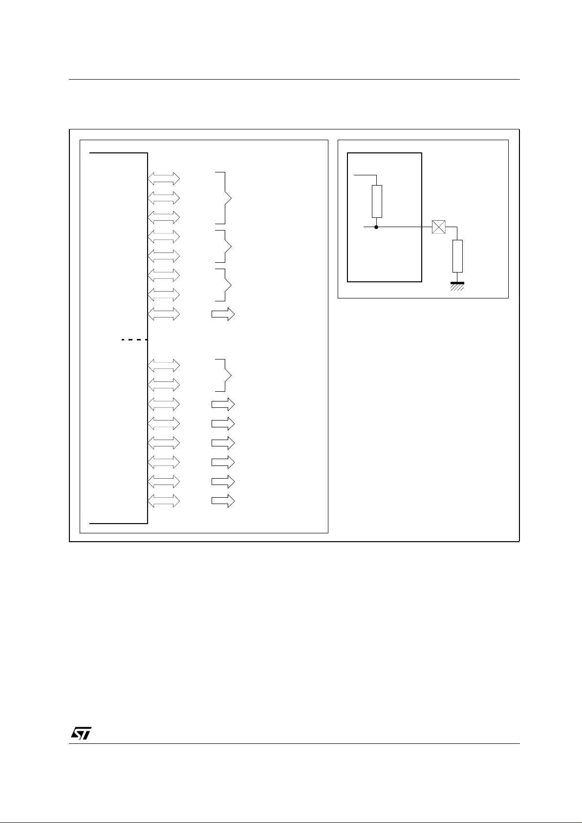
2.2 - PORT0 Start-up Configuration
Figure 4
PORT0 Pin Assigment for Power-on Configuration
P0H7
P0H6
P0H5
Clock Options
(Refer to datasheet /
user’s manual
for PLL factor
AN1544 - APPLICAT ION NOTE
V
DD
Internal
Pull Up
P0L pin
PORT0
P0H
P0L
P0H4
P0H3
P0H2
P0H1
P0H0
P0L7
P0L6
P0L5
P0L4
P0L3
P0L2
P0L1
P0L0
Segment address lines
Chip Selects
WR. Configuration
Bustype (BTYP)
Startup Configuration
Reserved
Bootstrap Loader Mode
Reserved
Reserved
Adapt Mode
Emulation Mode
Port0 during reset
External
Pull Down
Figure 3 is showing the usage of PORT0 pins to configure ST10F269. All pins are samp led at power-on
reset and some of them are not sampled for specific reset conditions. For details, please refer to the product datasheet and the AN1334 "ST10F269/ST10F280 System Reset" application note.
7/14
Page 8

AN1544 - APPLICAT ION NOTE
3 - FILTERING / DECOUPLING
3.1 - Decoupling on DC1 and DC2 Pins
DC1 and DC2 are the outputs of ST10F269 internal voltage regulator. They are available on the package
to connect external decoupling capacitors.
A capacitor, X7R dielectric or equivalent, with a minimum value of 330nF, must be connected bet ween
each of these pins and its nearest V
with the ground.
As DC1 and DC2 pi ns are internally connected, the voltage regulator sees an equivalent capacitor of
660nF. This is the minimum value that must be provided for correct operation. In case of space issue on
the PCB, the capacitors can be of different values provided that the biggest value is on DC1 (pin 56) (DC1
provides the feedback of the regulator). For example DC1 could be connected to a 470nF capacitor and
DC2 to a 220nF capacitor.
3.2 - Decoupling on +5V Supply
Decoupling capacitors shall be placed as close as possible to the chip V
– Connected to both V
– Connected to each V
and VSS pins (adjacent pins).
DD
DD/VSS
pair.
For EMC reasons, decoupling capacitors shall be connected to the V
illustrated by Figure 5 below :
Figure 5 :
Implementation of Decoupling Capaci tors
pin. This is done for decoupling the output of the internal regulator
SS
SS/VDD
and VSS of adjacent pins. This is
DD
pins,
Via to
V
DD
V
ST10F269
Good implementation
Cap.
DD
Via to V
Via to V
V
SS
SS
Implementation to be avoided
SS
ST10F269
Cap.
V
DD
Via to V
V
SS
SS
8/14
Page 9

AN1544 - APPLICAT ION NOTE
3.3 - Filtering / EMC
As ST10F269 has an internal voltage regulator, +5V pins are not differentiated between output-buffers
and internal logi c. This means that when EMC filters are used to isolate the CPU from the s upply, all
ST10F269 supply pins should be isolated with the filter(s).
Example of filter
Filter placed on supply line of the CPU to remove the conducted noise from the supply line of the module.
Figure 6 :
Filter Based on Discrete Components
ST10F269
+5V plane
L
pins
V
DD
C
L
GND plane
Filter connected to supply line of the CPU
C
V
pins
SS
3.4 - Unused Pins
Unsed pins may be an additional source of noise if not properly connected.
Unsed pins shall
NOT
be left floating.
They shall be :
– Connected to V
via external pull down resistors.
SS
– Configured by software as output (set direction bit to 0) with output=0 (data=0).
Note : Avoiding floating pins in an application also ensures a good control on power consumption.
9/14
Page 10

AN1544 - APPLICAT ION NOTE
4 - SPECIAL PINS
4.1 - EA
External Access Enable pin
. A low level applied to this pin during and after reset forces the ST10F2xx to start the program execution
from the external memory spac e. A high level will start the program execution from internal memory.
If only internal memory will be used, this pin can be tied directly to V
DD
.
4.2 - RPD Pin
RPD pin (Return from Power-Down) is used to generate the proper internal tim ing sequ enc e whe n interruptible power-down mode is used.
If not used, PRD pin can be tied to GND via a pull-down resistor (max = 1MΩ).
5 - RESET
For information on ST10F269 reset, pleas e refer to the AN1334 "ST10F269/ST10F280 Syste m Reset"
application note.
10/14
Page 11

AN1544 - APPLICAT ION NOTE
6 - ADC
Analog input signal error can be created by poor matching of the source internal resistance with the ADC
input parameters, either caused by,
– Voltage drop in the voltage source resistance due to input leakage current,
– Or by poor charging of the ADC internal capacitance (Cin).
– Analog input error can also be caused by noise from the analog input signal.
This section describes each of these causes.
Figure 7
Source Internal Resistance Errors
SAMPLE
V
P5.x
IN
R1
I
C
IO
OZ1
Leakage
Current
C
IN
R
SOURCE
V
S
AGND AGND
I
(Input leakage current Port5): maximum ± 200nA ( test Condition: 0.45V<VIN<VDD)
OZ1
(Pin capacitance Port5): max imum 10pF (test Condition: f = 1MHz, TA = 25°C, guaranteed by design characteri zation)
C
IO
(ADC Internal capacitance): maximum 5pF (guaranteed by design characterizati on)
C
IN
R1 (series input resistance): maxim um 1.5kΩ (guaranteed by design characterizati on)
6.1 - Voltage Drop in the Source Resistance
The error generated by the voltage source internal resistance is:
I
(OZ1)
–
.
×
()
×
R
SOURCEI0Z1
--------------------------------------------- 1024
=
V
I
(OZ1)
=
specified leakage current.
()
error LS B
Refer the latest product datasheet for the value of
AREFVAGND
Note Input leakage c urrent i s caused by parasitic current into the on-chip protection of t he input pin; this
protection is necessar y to prot ect the device against ES D (Elect rical Static Di scharg e) and a gainst overload.
6.2 - Poor Charging of the ADC Internal Resistance
During the sample time, the input capacitance (C
and CIN) must be charged/discharged by the external
IO
source. The internal resistance of the source must allow the capacitance to reach its final value before the
end of sample time:
If this does not happen, i.e. if the source resistance is misma tched to th e sampl e time, a voltage loss will
occur at the sample and hold stage. This voltage loss causes an accuracy loss when increasing or
decreasing the input voltage from Vref/2 (hold capacitor is pre-charged to Vref/2 before sampling to
redu c e charge/discharge t ime) .
The error is be calculated by the formula:
t
S
–
---------
1
---
1024 e
2
Where: t
= sample time in µs, R = R
S
Max·error
SOURCE
()
LSB
+ R1 in Ω, C = CIN + CIO in µF.
Since the error is proportional to the difference between V
ity in the conversion of large-amplitude signals. In practice, if t
RC
××=
and Vref/2, the effect produces a non-linear-
IN
>7RC, the maximum error is reduced to
S
<1/2 LSB (<0.05%).
11/14
Page 12

AN1544 - APPLICAT ION NOTE
6.3 - Errors Due to Hi gh Frequenci es from I nput Si gnal
Small but high frequency signal variations can result in increased conversion error: During sampling time,
the analog signal is fed to an internal auto-zero circuitry. Signal variations (2 opposite transitions at least)
during this time can generate auto-zero error. Signal variations during sampling time generate excessively high or low conversion results; big variations (ex: 150mV peak to peak variations at 1.5MHz, with a
2.5V offset for 1us sampling time) can generates clamped results (0x000 or 0x3FFh).
Although the sample and ho ld internal c ircuitry is integrating signal variations, other intern al analog cir-
cuitry can be affected by signal transitions during sampling time.
The input analog signal shall always be low pass filtered to ensure that high frequencies are
rejected.
6.4 - Reducing ADC Errors
There are four possible optimisations :
Minimise the total source impedance seen by the ST10:
This means choosing sensors with low output
impedance (not always easy for some types of sensor), and minimising the serial resistance of any protection devices between the analog source and the input pin (while still providing a voltage protection level
compatible with the circuit specification).
Match the sample time to the analog source impedance:
Use the formula that relates sample time to
source interna l resistance (given in the ST10 datasheet) to match the source resistance to one of the
available sample times.
For example: With a source impedance of 10KΩ, and given
R
= ts / 330 - 0.25
ASRC
then the minimum sample time is:
t
= 330 x (R
s
= 3380ns(min)
t
s
ASRC
+ 0.25)
Note: This formula includes a safety factor of 10, therefore, dynamic errors are ≈0.02LSB.
Also, R
is the total source impedance seen by the device and, therefore, includes any pro-
ASRC
tection components.
Match the sample time to the analog filter cut-off frequency to remove high frequencies :
the
ST10F269 sampling time (ADC s ilic on configur ati o n) shall be 5 to 10 time s sho rte r tha n the pe riod of the
cut-off frequency of the low-pass filter on ADC input signal.
Reduc e noise at the inpu t pin:
Add an external RC filter (with attention to the source internal resis-
tance). Comput the average value of different samples in the software routine.
For details, see the AN1538 "ST10F269/ST10F280 : Reducing Analog -Digital Conversion Error" applica-
tion note.
6.5 - Varef Power-up / Down Sequence
Varef should always be lower than the 5V supply (maximum = V
+0.1v). This is especially true for
DD
power-up and power-down sequence when external devices are used to generate Varef.
7 - EXTERNAL MEMORY INTERFACE
ST10F269 external memo ry bus can easily interface with STMicroelectronics external Flash (M29Fxx
series).
Please, refer to application note AN1155 "Connecting the ST10 Microcontroller to M29 Series Flash
Memories."
12/14
Page 13

AN1544 - APPLICAT ION NOTE
8 - CONNECTING TO L4969
L4969 is a combined voltage regulator and low-speed CAN interface from STMicroelectronices.
The following figure shows how to connect the L4969 CAN interface to the ST10F269/ST10F280 micro-
controller when working on a SPI bus with multiple peripherals.
Note: For further information to the L4969 please refer to the L4969 datasheet and the available applica-
tion notes for this device.
When no other periph erals are connected to the SPI bus, the L4969 can be directly connected to the
ST10 SPI lines without any further constraints.
Figure 8 :
ST10F269 Connected to L4969 and other SPI Devices
RESET
Px.y
CS
L4969
CS
x
CS
y
SCLK
MTSR
MRST
EN
NRES
NINT
CLK
EN
L4969
SOUT
Device x Device y
SIN
9 - REVISION HIST ORY
9.1 - Creation of the AN1544 on the 24th of May 2002
9.2 - Revision of the AN1544 on the 24th of June 2002
Modification of the 1st sentence of section 6.3 p12, "can result in increased conversion error:" .
13/14
Page 14

AN1544 - APPLICAT ION NOTE
Information furnished is bel ieved to be accurate and reliable. However, STMicroe lectronics assumes no responsibility for the
consequences of use of such information nor for any infringement of patents or other rights of third parties which may result from
its use. No li cense is granted by i mp lication or otherwise under any patent or pate nt rig hts of STMicroelectronics. S pec ific at ions
mentioned in this publication ar e subject to change without notice. This publication supersedes and replaces all information
previously supplied. S TMicroelectronics products are not authorized for use as critica l components in life suppo rt devices or
systems without express written approval of STMicroelectronics.
The ST logo is a registered trademark of STMicroelectronics
© 2002 STMicroelectronics - All Rights Reserved
STMicroele ct ronics GROUP OF C OM P A NI ES
Australia - Brazi l - Canada - Ch i na - F i nl and - France - Germany - Hong Kong - India - Israel - Italy - Japan - Malays i a - M al ta - Morocco
Singapor e - S pai n - Sweden - S wi t zerland - U ni t ed Kingdom - U ni ted States
http://www.st.com
14/14
 Loading...