

Page 1
AN1542
®
THE THERMAL RUNAWAY LAW IN SCHOTTKY
INTRODUCTION
Nowadays,somecriticalapplicationsrequirevery
high available power supplies. Typically, these
applications are servers or telecommunication
base stations.
In such systems, the power supplies are built with
several power supplies connected in parallel in
order to be fault tolerant. Thanks to redundancy,
the total failure rate stays very low and the availability can exceed 99.99%.
The connection of several power supplies needs
the OR function, commonly built with diodes, to
tolerate faults in the SMPS.
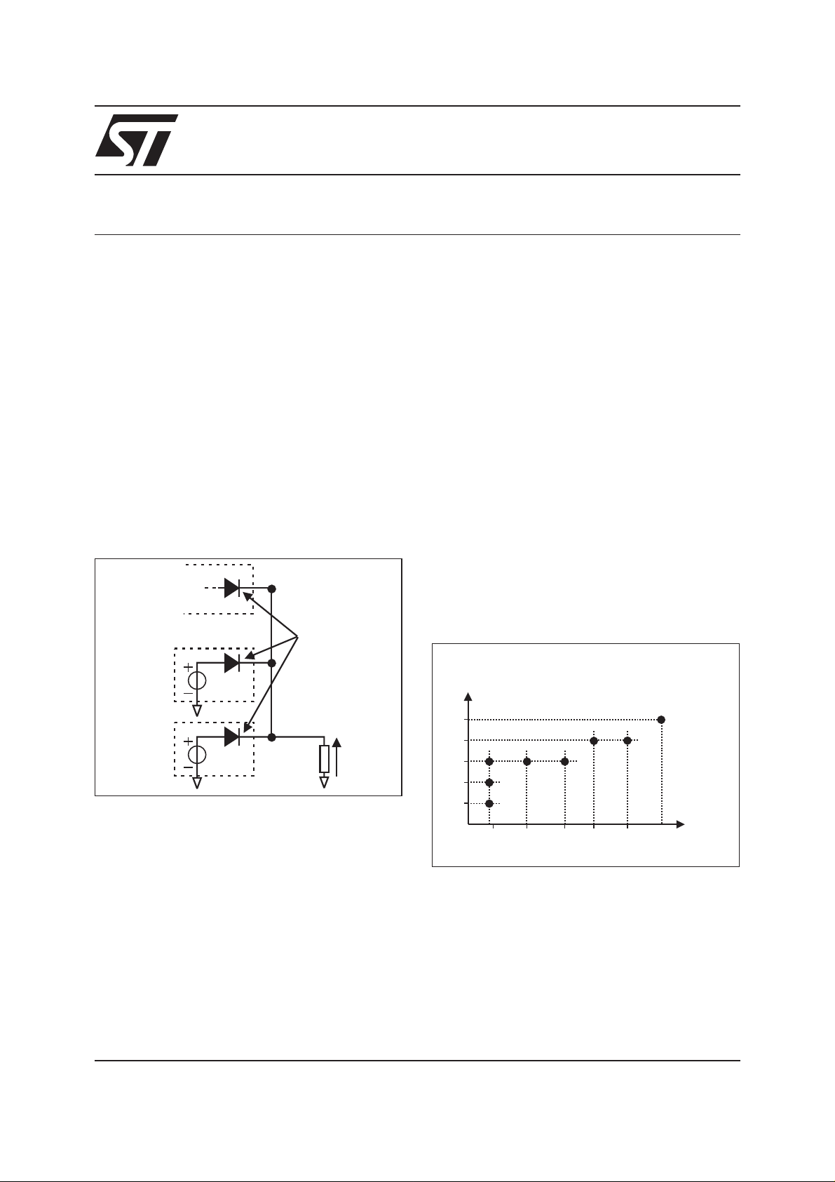
Fig. 1: Supplies connected in parallel
APPLICATION NOTE
USED IN OR-ing APPLICATION
by Y.LAUSENAZ
2. TYPICAL PREFERRED DEVICE
In normal operation the diode is conducting in
forward mode. So, the first requirement of the
component,irrespectiveof the maximum repetitive reverse voltage (V
ing (I
), is the forward voltage drop (VF).
F(AV)
The lower the forward voltage drop, the lower the
forward losses in the diode, and the better the
SMPS efficiency.
For this reason, Power Schottky diodes are commonly used in OR-ing application. The L series
(for example STPS60L30CW) are optimized to
provide very low forward voltage drop:
= 0.33V (30A @125°C per diode).
V
F typ
The following graph presents the typical Schottky
used in OR-ing application on common voltage
outputs:
) and the current rat-
RRM
Or function
SMPS 2
SMPS 1
Load Vout
1. OR-ing FUNCTION PRESENTATION
TheOR-ing function iscommonlybuilt with diodes.
The diodehasto let the current pass through when
the associated SMPS is working in normal operation. When a SMPS fails in short circuit, the diode
has to block reverse voltage in order to maintain
output voltage on the load.
The purpose of the OR function is to prevent fault
propagation between supplies connected in parallel.
Fig. 2: Typical Schottky used as OR-ing function
on common voltage outputs
Output
voltage
48V
24V
12V
5V
3.3V
L15 L30L25 L45 L60 H100
Schottky
voltage
Using Schottky diodes provides very low forward
losses.But the mainimportanttechnology trade off
for Schottky is between forward voltage drop and
leakage current:
The optimization of forward voltage drop is inevitably made to the detriment of leakage current.
High leakage current gives rise to the thermal
runaway problem.
May 2002
1/6
Page 2
APPLICATION NOTE
3. THERMAL RUNAWAY RISK
The risk of thermal runaway comes from the fact
that leakage current increases quickly with the
junction temperature.
3.1. Problems
Using a Schottky as OR-ing function provides a
very low forward voltage drop. But when the diode
is blocking because its associated supply has a
fault in short circuit mode, the diode has to operate
in reverse mode with high junction temperature
(due toprecedingforwardlosses) and so with relatively high reverse current.
This high reverse current can generate high reverse losses, and so increase junction temperature, and so reverse current as well… This is the
thermal runaway phenomenon.
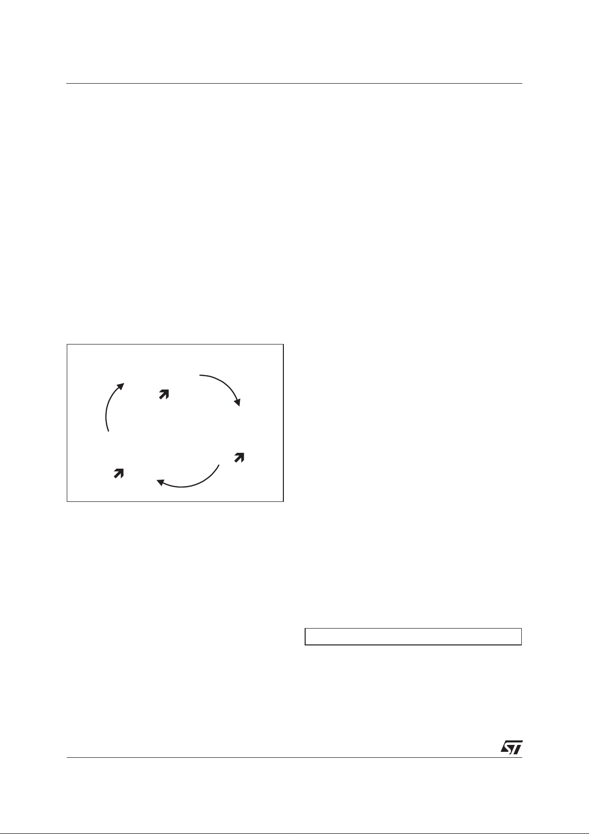
Fig. 3: Thermal runaway diagram
Reverse
current
Reverse
Junction
losses
temperature
The problem is to quantify the risk of thermal
runaway in order to prevent it.
3.2. Result in classical cases
In the classical simple case where both the following
assumptions are made:
Constant thermal resistance system
■
OR-ing diode on its own heatsink
■
The reverse losses in the Schottky diode, due to
associated SMPS short circuit failure, is a monotonous function of the time. Consequently the
thermal runaway diagram of fig. 3 is covered in
only one rotation- sense.
To determine if the Power Schottky will goes into
thermal runaway mode consists of finding the elements that will determine the rotation sense of
fig. 3.
During the forward mode, the forward current (I
defines the junction temperature (T
forward voltage (V
) and ambient temperature (T
R
th(j-a)
TT R IxV
=+
jambthjaFFI
), device thermal resistance
F
()
−() @
) (linked to
j
):
amb
fwd
F
During the fast mode change of the diode (from
the forward mode to the reverse one, the change
is fast in comparison to device thermal constant),
the junction temperatureduetothepreceding forwardmode stay continuous (c.f.fig.5) and willdetermine the leakage current (I
reverse voltage V
ITV I CV e
;;=°×
()( )
rev j rev rev rev
rev
):
100
) (linked to the
rev
−°
100
cT C
(
j
)
c ≈ 0.055°C-1(thermal constant)
This reverse current will determine the new junction temperature trend (linked to reverse voltage
and device thermal resistance). This variation
trend between the initial junction temperature (due
to forward mode) and the new one (due to reverse
mode)givesthe T
variationandthe rotation-sense
j
in fig. 3.
In a constant thermal resistance system, the ther-
mal stability can be determined by comparing forward losses (P
before the SMPS failure (t
losses (P
) occurring just after (t0+δt) the even-
rev
) in the power Schottky just
fwd
-δt) and the reverse
0
tual SMPS short-circuited fault.
)
2/6
The stability can be guaranteed if P
fwd>Prev@t0
Page 3

APPLICATION NOTE
Fig. 4: Typical loss variation in the OR-ing before
and after the SMPS failure
losses
Forward
mode
Reverse
mode
Thermal
runaway
Pfwd
Prev
SMPS
break down
t
0
Monotonous variation
time
Fig. 5: Typical junction temperature variation in
the OR-ing before and after the SMPS failure
Tj
Forward
mode
continuous
variation
Reverse
mode
Thermal
runaway
Fig. 6: Example of junction temperature variation
in non-constant thermal resistance system
Tj
Forward
mode
continuous
variation
SMPS
break down
t0
Reverse
mode
Fan switch
OFF
T
amb
NON-monotonous variation
Thermal
runaway
time
In these more complicated cases, device thermal
behavior can be simulated with tools like PSPICE.
The following analogies have to be used:
Thermal: Electrical:
Temperature Voltage
Power Current
Resistance Resistance
SMPS
break down
Tamb
time
Monotonous variation
3.3. Results in more complicated cases
More complicated cases, where the assumptions
of §3.2 do not exist, can be considered.
For example:
■
OR-ing diode not on its own heatsink.
The OR-ing diode can be mounted on common
heatsink with other dissipative devices. In this
case, the junction temperature of the OR-ing diode can be influenced by the other devices,
thanks to coupling thermal resistance.
■
Non constant thermal resistance system:
The convection can be forced by a fan connected to the Anode side of the OR-ing diode. In
case of SMPS failure, the fan will stop and the
R
will increase. In this case, the junction
th(j-a)
temperature variation will not be monotonous.
Fig. 7: Thermal / electric analogy for simulation
Junction
P (losses)
Rth(j-c)
Rth(c-a)
Tamb
Tjunction
Case
Tcase
Ambiant
This analogy can be use to analyze any complex
thermal problem.
3/6
Page 4

APPLICATION NOTE
4. FROM THERMAL RUNAWAY TO PRODUCT
OPTIMIZATION
STMicroelectronics has developed a Schottky
family dedicated to the OR-ing function. This “L”
family demonstrates very low forward voltage in
orderto reduce conduction losses. Consequently,
the leakage current is relatively high.
For example, the “L15" family (V
=15V) is op-
RRM
timized for 3.3V, 5V and eventually 12V output
as OR-ing diode.
Due to the specific thermal runaway law of the
Schottky in OR-ing application, we can optimize
the device choice in order to improve the SMPS
efficiency, while keeping the risk of thermal runaway under control.
For example, let’s take a 3.3V 35A output, with a
STPS40L15C as OR-ing diode. The two diodes
have to be considered like connected in parallel:
Fig. 8: SMPS output synopsis
STPS40L15C
I = 35A (=2I )out fwd
V = 3.3Vout
P V I T V diodes in parallel
=× ⋅
2332
rev out rev j
V
=× ⋅
2
out
1
c C thermal cons
0 055
š
.
I C V per diode datasheet
100 3 3° ;. ( , )
()
rev
−
;. ( )
()
100
−°
cTj C
ICVe
100 3 3
°×
()
rev
()
;.
tan
(
t
)
Note that it is very important to use maximum reverse current values to evaluate reverse losses.
Actually, the worst case must be considered to
evaluate junction temperature in order to be sure
to avoid thermal runaway.
The limit of the thermal runaway criteria being defined by P
ture T
PVICVe
rev out rev
T
j
max
fwd=Prev
corresponds to P
j max
=× ⋅ ° ×
2 100 3 3
max
00
°+
=
1
137
=°
, the maximal junction tempera-
rev max=Pfwd
;.
P
fwd
×⋅ °
VI C V
()
out rev
C
()
1
In
2 100 3 3
c
C
:
−°
100
cT C
(
j
max
;.
The maximum junction temperature reachable in
forward mode before the risk of thermal runaway
occurs is so high, that we can consider a well
adapted device. This one will have a lower forward
voltage so a highest reverse current.
The same process can be applied to different
devices
)
P = 115.5Wout
In the forward mode, the forward losses can be
calculated as:
PVIRI
=× ⋅ + ⋅
2
fwd T fwd d fwd
()
0
.. (
=× +
2 018 8 010
.= 11 2
IId
()
fwd fwd
W
Theses losses decrease the global SMPS efficiency about 9.7%.
The risk of thermal runaway can be evaluated by
calculating the maximum junction temperature
that must not be reached in forward mode to
avoid reverse losses being higher than forward
losses, thus avoiding thermal runaway.
2
−
32
atasheet
STPS80L15C
Forward losses P
fwd
= 9.0W
The efficiency loss about 7.8%.
Maximal junction temperature before thermal runaway: T
jmax
= 127°C
STPS120L15
Forward losses: P
fwd
= 7.6W
The efficiency loss is about 6.6%
Maximal junction temperature before thermal run-
)
away: T
= 100.3°C
jmax
STPS20L15 (the 20A average current specified is
only indicative value)
Forward losses: P
= 16.1W
fwd
The efficiency loss is about 13.9%
Maximal junction temperature before thermal runaway: T
= 155.9°C
jmax
The comparison between the 4 parts considered
on the 3.3V 35A output can be summarized on the
following graph:
4/6
Page 5

APPLICATION NOTE
Fig. 9: Comparison between 4 parts, forward
losses, efficiency loss and T
Efficiency
Forward
16.1W
11.2W
9.0W
7.6W
losses
loss
13.9%
T = 156°Cjmax
9.7%
7.8%
6.6%
STPS L1520 STPS L15C40 STPS L15C80 STPS L15120
T = 137°Cjmax
.
jmax
V = 3.3V
I = 35A
T = 127°Cjmax
out
out
T = 100.3°Cjmax
Using the specific thermal runawaylaw,theSMPS
designer can optimize the OR-ing diode choice in
order to improve the global efficiency.
The risk of thermal runaway is controlled by limiting
the junction temperature during the forward mode
below the maximum value evaluated.
CONCLUSION
STMicroelectronicsisdeveloping “L” family diodes
dedicated to the OR-ing application. This family
shows very low forward voltage in order to reduce
conduction losses and to improve efficiency:
STPSXXL15, STPSXXL25, STPSXXL30,
STPSXXL45, and STPSXXL60.
With the very simple law presented, it becomes
straightforward to optimize devices choice by
evaluating the risk of thermal runway in Schottky
used in OR-ing function in SMPS.
This reliable and accurate law allows the optimization of the devices used in order to improve
converter efficiency while controlling the risk of
thermal runaway risk.
ANNEXE: EVALUATION OF MAXIMUM REVERSE CURRENT FROM DATASHEET
To evaluate the limit before thermal runaway, the
maximum value of the reverse current has to be
considered. Actually, this parameter is critical for
thermal runaway and the worst case must be considered.
To evaluate the maximum reverse current of a
power Schottky, take the typical value given in
figure. Apply the ratio between typical and maximal value given in the table (in the adapted V
and Tjfield). Finally, use the adapted formula to
get the expected junction temperature.
Example: STPS80L15C (twin diode in parallel)
under 3.3V @125°C
Figure 5 of the STPS80L15C datasheet gives the
typical value of the reverse current @100°C for
3.3V (per diode):
Fig. 5: Reverse leakage current versus reverse
voltage applied (typical values
IR(mA)
1E+3
1E+2
1E+1
220mA
1E+0
1E-1
0123456789101112131415
(100°C ; 3.3V) = 220mA
I
rev typ
Tj=100°C
Tj=75°C
Tj=25°C
3.3V
, per diode).
VR(V)
Thestatic electrical characteristics tablegives the
ratio between typical and maximum values (per
diode):
STATIC ELECTRICAL CHARACTERISTICS (per diode).
Symbol Parameter Tests conditions Min. Typ. Max. Unit
* Reverse leakage
I
R
current
Pulse test :*tp=380µs,δ <2%
Tj=25°CVR=5V 4 mA
Tj = 100°C 280 400
Tj=25°CV
Tj = 100°C 0.44 1.1 A
Tj=25°CV
Tj = 100°C 0.53 1.3 A
= 12V 11
R
= 15V 16 mA
R
R
5/6
Page 6

APPLICATION NOTE
ICV mA
()
rev
max
;.100 3 3 220
400
280
314°=×=
IT V I C V e
()
Thefollowingformula allows the calculation ofthe
reverse current in a power Schottky for every
junction temperature from a reference value:
ICVICVe
100
−°
cTj C
;. ;.
33 100 33
()( )
rev j rev
cCth
.
0 055
š
125 3 3 100 3 3
()()
rev rev
=° ×
1
−
ermal cons t
°=°×
;. ;.
A
12
=
.
tan
(
)
125 100
−
c
(
So, the global maximum reverse current value for
the two diodes of the STPS80L15C connected in
parallel under 3.3V @125°C is:
)
ICVA
125 3 3 2 12
()
rev
max
;. .
°=×
A
.
24
≈
Information furnished is believed to be accurate and reliable. However, STMicroelectronics assumes no responsibility for the consequences
ofuse of such informationnor for any infringementof patents or otherrights of third partieswhich may result fromits use. No licenseis granted
by implication or otherwise under anypatent or patent rights of STMicroelectronics. Specifications mentioned in this publication are subjectto
change without notice. This publication supersedes and replaces all information previously supplied.
STMicroelectronics products are not authorized for use as critical components in life support devices or systems without express written approval of STMicroelectronics.
The ST logo is a registered trademark of STMicroelectronics
© 2002 STMicroelectronics - Printed in Italy - All rights reserved.
STMicroelectronics GROUP OF COMPANIES
Australia - Brazil - Canada - China - Finland - France - Germany
Hong Kong - India - Israel - Italy - Japan - Malaysia - Malta - Morocco - Singapore
Spain - Sweden - Switzerland - United Kingdom - United States.
http://www.st.com
6/6
 Loading...