

Page 1

AN1538
APPLICATION NOTE
Reducing Analog-Digital Conversion Error Using
ST10F269/ST 10F 280
By André ROGER
INTRODUCTION
The ST10F269/ST10F280 contains an Analog / Digital Converter with 10-bit resolution, 4.85µs
conversion time, a sample & hold circuit on-chip, ESD protected anal og inputs and a “Total Unadjusted
Error” of ± 2LSB across the whole automotive temperature range.
This application note identifies the causes of ADC error and gives solutions to optimize ADC
performance. An appendix reviews the meaning of the terms: resolution, accuracy and intrinsic error.
1/8March 2002
Page 2

AN1538 - APPLICAT ION NOTE
TABLE OF CONTENTS PAGE
1 SOURCES OF ADC ERROR ..................................................................................... 3
1.1 ANALOG INPUT SIGNAL ERROR ............................................................................. 3
1.1.1 Source Internal Resistance Matching with ADC Input Parameters ... ......................... 3
1.1.2 Errors Due to High Frequencies from Input Signal ..................................................... 5
1.2 INPUT OVERLOAD ERRORS ....... ................ ................. ........................ ................ ... 5
1.3 REFERENCE VOLTAGE ERRORS ........................................................................... 5
1.3.1 Reference Voltage Accuracy and Absolute Tolerance on a Conversion Result ......... 5
1.3.2 Reference Voltage Accuracy and Differential Tolerance on Conversion Results . ...... 5
2 HOW TO MINIMIZE ERROR ...................................................................................... 6
2.1 OPTIMISE THE INPUT SIGNAL ................................................................................ 6
2.2 REDUCE INPUT OVERLOAD ERROR ...................................................................... 6
2.3 REFERENCE VOLTAGE ERROR REDUCTION ....................................................... 7
3 APPENDIX DEFINITIO N S ........................... ........................ ................ ................. ..... 8
4 REVISION HISTORY ......................... ................. ................. ................ ...................... 8
4.1 CREATION OF THE AN1538 ON THE 14TH OF MARCH 2002 ............................... 8
2/8
Page 3
AN1538 - APPLICAT ION NOTE
1 - SOURCES OF ADC ERROR
Sources of ADC accuracy error are classified into 3 categories:
– Analog input signal error
– Input overload error
– Reference voltage error
Each of these categories is describ ed in the following sections.
1.1 - Analog Input Signal Error
1.1.1 - Source Internal Resistance Matching with ADC Input Parameters
Analog input signal error can be created by poor matching of the source internal resistance with the ADC
input parameters, either caused by,
– Voltage drop in the voltage source resistance due to input leakage current,
– Or by poor charging of the ADC internal capacitance (Cin).
Analog input error can also be caused by noise from the analog input signal. This section described each
of these causes.
Figure 1 :
Source Internal Resistance Errors
SAMPLE
V
P5.x
IN
R1
I
C
IO
OZ1
Leakage
Current
C
IN
R
SOURCE
V
S
AGND AGND
I
(Input leakage current P ort5) : maximum ± 200 nA (test Condition: 0.45V<VIN<VDD)
OZ1
C
(Pin capacitance Port5): maximum 10 pF (test Condition: f = 1 MHz, TA = 25°C, guaranteed by design characterization)
IO
(ADC Internal capacitance): maximum 5 pF (guaranteed by design characterization)
C
IN
R1 (series input resistance): maximum 1.5kΩ (guaranteed by design characterization)
Refer to Figure 1 for a schematic of source internal resistance errors.
Static voltage drop in the source resistance:
The error generated by the voltage source internal
resistance is:
For example :
R
error
()
LSB
SOURCEI0Z1
---------------------------------------------- 1024×=
V
AREFVAGND
A source resistance of 15KΩ and a specified leakage current (I
×
–
) of ±500nA will cause
OZ1
a static voltage error of ±7.5mV or ±1.5LSB.
Refer the latest product datasheet for the value of
I
OZ1
.
Notes: 1. Input leakage c urrent is caused by parasitic current at input pin protection; this protection is
necessary to protect the device against ESD (Electrical Static Discharge) and against overload.
2. Adding a filter ing capaci tor at the ana log input pin do es not chan ge the static voltage drop; it
only improves the charging time of the internal capacitors (see after).
3/8
Page 4

AN1538 - APPLICAT ION NOTE
Poor charging of the ADC internal capacitance:
During the sample time, the input capacitance (C
IO
and CIN) must be charged/discharged by the external source. The internal resistance of the source must
allow the capacitance to reach its final value before the end of sample time:
Figure 2 :
Possible Error Due to Input Capacitance Charging
Voltage at sam ple and
hold input
V
IN
V
/2
ref
t
s
time
V
err
Voltage error at time t
i
time
If this does not happen, i.e. if the source resistance is mis-matched to the sample time, a voltage loss will
occur at the sample and hold stage. This voltage loss causes an accuracy loss when increasing or
decreasing the input voltage from Vref/2 (hold capacitor is pre-charged to Vref/2 before sampling to
redu c e cha rge/disc harge t ime) .
The error is be calcuated by the formula:
t
S
–
-------- -
1
-- - 1024 e
2
Where: t
= sample time in µs, R = R
S
Max·error
SOURCE
()
LSB
+ R1 in Ω, C = CIN + CIO in µF. For example:
Since the error is proportional to the difference between V
non-linearity in the conversion of large-amplitude signals. In practice, if t
RC
××=
and Vref/2, the effect produces a
IN
>7RC, the maximum error is
S
reduced to <1/2 LSB (<0.05%).
Errors due to noise from the input signal :
The sample and hold circuitry is not designed to filter the
input analog sign al. Noise at the input signal will cause input voltage variation and, therefore, accuracy
loss.
4/8
Page 5

AN1538 - APPLICAT ION NOTE
1.1.2 - Errors Due to High Frequencies from Input Signal
Small but high frequency sign al variations can result in big conversion errors : During sampli ng tim e, the
analog signal is fed to an internal a uto-zero circuitr y. Signal variations (2 opposite t ransitions at least)
during this time can generate auto-zero error.
Signal variations during sampling time generate excessively high or low conversion results; big variations
(ex : 150mV peak to peak variations at 1.5MHz, with a 2.5V offset for 1µs sampling time) can gen erates
clamped results (0x000h or 0x3FFh).
=> Allthough the sampl e and hold internal circuitry is integrating signal variations, other inter nal analog
circuitry can be affected by signal transitions during sampling time,
The input analog signal sh all always be low pass filtered to ensure that high frequ encies are
=>
rejected
1.2 - Input Overload Errors
These errors are caused by input overload. During overload, intern al protection-diodes sink current to
reduce the overload voltage. Because of the close proximity of the internal protection-diodes and the
ADC circuitry, the ADC performance is affected.
The ST10F269/ST10F280 accepts up to 10mA of input overload current while guaranteeing a Total
Unadusjted Error (TUE) of ± 2LSB (refer to the product Data sheet for values).
Overload above the specified limit causes ADC accuracy loss and may damage the circuit.
1.3 - Reference Voltage Errors
The accuracy of the conversion is obviously linked to the accuracy of the reference voltage.
.
1.3.1 - Reference Voltage Accuracy and Absolute Tolerance on a Conversion Result
To com put e t he acc uracy o n conversion result, the accuracy on the reference voltage must be taken into
account.
1.3.2 - Reference Voltage Accuracy and Differential To lerance on Conversion Results
For differential computing (ie : difference between conversions), only the stability of the reference voltage
is to take into accou nt. When the analog voltage is der ived from a voltage regulator, the accuracy on
voltage reference is given by the rejection factor of the regulator and the maximum voltage variation that
is possible between the 2 conversions.
Tem perature : Temperature coupling effect may be neglected if the time between the 2 sam ples is shor t
compared to the thermal constant.
While noise and/or voltage variations are a well known source of error, internal resistance is another
source of error from the reference voltage.
During the conversion, the ADC internal capacitance must be repeatedly charged or discharged. The
internal resistance of the reference voltage must allow the capacitance to reach its correct voltage within
the conversion time (see figure below). A mis-match between the conversion time and reference voltage
internal resistance will cause accuracy errors.
Figure 3 :
Simplified Circuit for Analog Reference Voltage
P
5.X
R
REF
V
AREF
V
IN
ADC
V
REF
V
AGND
5/8
Page 6

AN1538 - APPLICAT ION NOTE
2 - HOW TO MINIMIZE ERROR
2.1 - Optimise the Input Signal
There are four possible optimisations :
Minimise the total source impedance seen by the ST10:
impedance (not always easy for some types of sensor), and minimising the serial resistance of any
protection devices between the analog s ource and t he input pin (while still providing a voltage protection
level compatible with the circuit specification).
Match the sample time to the analog source impedance:
source interna l resistance (given in the ST10 datasheet) to match the source resistance to one of the
available sample times.
For example: With a source impedance of 10kΩ, and given
This means choosing sensors with low output
Use the formula that relates sample time to
R
ASRC
t
330)0.25–⁄=
(
S
then the minimum sample time is:
330 R
t
S
3380ns min()=
t
S
ASRC
0.25+()×=
Note: Th is formula includes a safety factor of 10, therefore, dynamic errors are ≈0.02LSB.
Also, R
is the total source impedance seen by the device and, therefore, includes any
ASRC
protection components.
Match the sample time to the analog filter cut-off frequency to remove high frequencies :
the
ST10F269/ST10F2 80 sampling time (ADC silicon con figuration) shall be 5 to 10 times shor ter than t he
period of the cut-off frequency of the low-pass filter on ADC input signal.
Reduce noise at the input pin:
Add an external RC filter (with attention to the source internal
resistance). Comput the average value of different samples in the software routine.
2.2 - Reduce Input Overload Error
Because errors are induced from overload current going into/out of the integrated protection diodes,
optimisations minimize this current in 3 ways:
Minimize the overvoltage at the analog source:
The possible optimisations depend on the user
application, typically , they in volv e the addition of zener diodes or transils. For component selection, please
refer to ST-On-Line Discrete Devices / Protection Circuit Data Books.
Minimize the overvoltage at the S T10 analog inp ut pins:
Either, add protection diode(s) or transil(s),
or add a serial resistor. CA UTION: the addition of a serial resistor increases the source internal resistance
and, therefore, may impact maximum conversion speed.
Synchronise ADC conversion with analog transitions:
Where possible, avoid carrying out
conversions when analog inputs are scheduled to go into overload conditions (at least, during the
transition phase).
6/8
Page 7

AN1538 - APPLICAT ION NOTE
2.3 - Reference Voltage Error Reduction
The possible optimisations are :
Reference voltage noise:
reference voltage:
- Place the analog-reference source as close as possible to the V
- Avoid routing any high frequency/high amplitude signals near to the analog source.
- Make sure that the Voltage Reference source presents a low impedance from DC to well above the max.
sampling frequency (1/t
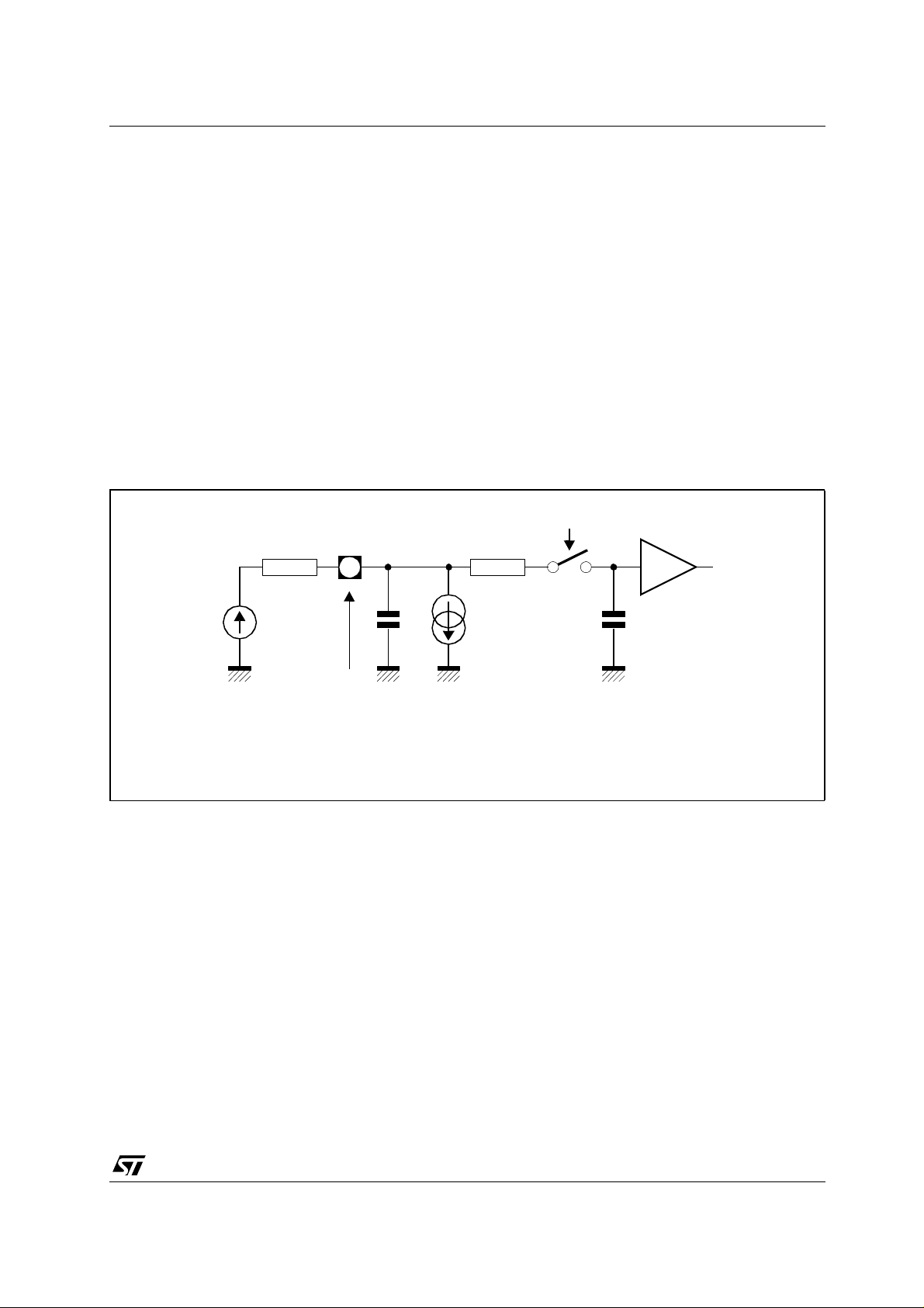
Figure 4 :
Analog Reference Source - Impedance Characteristics
Noise can be reduced by carefull design, PCB routing and dec oupling of the
pin.
AREF
):
c
Z
AREF
10/t
c
Match the reference voltage internal re sistance to conversion time:
ƒ
Use the formula that relates
conversion time to source internal resistance (given in the ST10 datasheet) to match the reference
voltage to one of the 3 available conversion times.
For example: given
t
--------- - 0.25–=
165
1200
------------ - 0.25–=
165
7kΩ max()=
20µs, Z
V
CC
< 7kΩ, up to 500k
AREF
AREF
Z
AREF
= R//
1
------------
JωC
then the maximum source impedance for t
Note: This should hold up to f=10/t
Figure 5 :
Typical Analog Reference Circuit
, so if t
C
R
R
AREF
of 1200ns is:
cc
R
AREF
≈
C
C
V
AGND
Figure 5 shows a comm only used circuit for the analog reference voltage.
7/8
Page 8

AN1538 - APPLICAT ION NOTE
3 - APPENDIX - DEFINITIONS
LSB :
Least Significant Bit.
Resolution :
between one code and the next adjacent code. Resolution is a design parameter rather than a
performance specification; it says nothing about accuracy. Resolution is either expressed in percent of the
full-scale, or in binary bits.
Accuracy :
equivalent of the binary output code. For ST10 devices, the Total Unadjusted Error describes the
maximu m s um of all errors int risic to the ADC.
Intrisic errors :
hysteresis error, linearity error. For simplicity and ease of use, the ST10 ADC specification gives the sum
of all intrisic errors (Total Unadjusted Errors).
4 - REVISION HIST ORY
4.1 - Creation of the AN1538 on the 14th of March 2002
defines the smalle st input voltage change re quired to increment the output of the ADC
defines the worst case difference between the actual input voltage and the full-scale weighted
are errors intrisic to the ADC itself, such as: quantizing error, scale error, offset error,
Information furnished is bel ieved to be accurate and reliable. However, STMicroe lectronics assumes no responsibility for the
consequences of use of such information nor for any infringement of patents or other rights of third parties which may result from
its use. No li cense is granted by i mp lication or otherwise under any patent or patent rights of STMicroelec tron ic s. S pec ificat ions
mentioned in this publication ar e subject to change without notice. This publication supersedes and replaces all information
previously supplied. S TMicroelectronics products are not authorized for use as critica l components in life suppo rt devices or
systems without express written approval of STMicroelectronics.
The ST logo is a registered trademark of STMicroelectronics
© 2002 STMicroelectronics - All Rights Reserved
STMicroele ct ronics GROUP OF C OM P A NI E S
Australia - Brazi l - Canada - China - Finland - France - Germ any - Hong Kong - India - Israel - Ita l y - J apan - Malaysia - Malt a - Morocco
8/8
Singapor e - S pai n - Sweden - S witzerland - United Kingdom - Unit ed S tates
http://www.st.com
 Loading...