

Page 1

AN1537
APPLICATION NOTE
A SIMPLE TRICK ENHANCES
L5991’s STANDBY FUNCTION
by C. Adragna and G. Gattavari
This application notes describes a simple technique that allows improving the Standby function of the
advanced PWM controller L5991. The price to pay for that is the addition of just two resistors and two
diodes, but the benefit brought in terms of no-load consumption in mains-operated converters is worth
this small fee. The effectiveness of the improved Standby function will be proved and assessed on a
couple of existing designs.
Introduction
L5991's Standby function is a valuable help in reducing light-load input consumption of offline converters and
making them compliant with energy saving standards such as EnergyStar, Energy2000 and others. This function, optimized for flyback topology , is the ability of automatically - and abruptly - reducing the osc illator frequency (i.e. converter's switching frequency) as the converter's load falls below a defined thr eshold and restoring the
normal oscillator frequency as the load increases and exceeds a second threshold.
The frequency shift allows minimizing power losses related to switching frequency, which represent most of
losses at light or no load, without giving up the advantages of a higher switching frequency at full load.
Being the L5991 a current-mode controller [1], the output voltage (V
except for an offset, is proportional to the peak pr imary current and then to the ener gy handled by the transformer cycle by cycle. It is then possible to deduce converter's load conditions by monitoring V
) of its error amplifier (pin 6, COMP),
COMP
.
COMP
Figure 1. L5991's Standby function operation:
fsw
fosc
fSB
Standby
1234
V
T
1
VCOMP
Normal operation
V
T
2
If the peak primary current decreases as a result of a decrease of the pow er demanded by the load and V
fsw vs.
V
locus (left) and
COMP
Pin
PNO
PSB
1234
V
COMP
Undershoot
during transition
V
T
1
VCOMP
vs.
Pin locus (right).
Normal operation
Standby
Overshoot
during transition
V
T
2
fosc
fSB
COMP
falls below a fixed threshold (VT1), the oscillator frequency will be set at a lower value (fSB). If now the peak
primary current increases and V
reset at the normal value ( f
). Since the frequency shift causes V
osc
for energy balance reasons, an appropriate hysteresis (V
from switching back and forth between f
The L5991 allows programming both the normal and the standby frequency. V
exceeds a second threshold (VT2 > VT1) the oscillator frequency will be
COMP
SB
and f
) is provided to prevent the oscillator frequency
T2-VT1
. This operation is shown in fig. 1.
osc
to shift too but in the oppos ite direc tion
COMP
and VT2 are internally fixed but
T1
May 2003
1/18
Page 2
AN1537 APPLICATION NOTE
it is possibl e to adjust the thresholds in terms of input power level (PNO, PSB) by adding a DC offset on its curr ent
sense input (pin 13, ISEN). Reference [2] provides plenty of details on this function and its usage.
There is a maxi mum abrupt frequency shift a llowed, wh ich i s relate d to the amount of hysteresis: the theoretic al
maximum ratio of f
during the transients resulting from the frequency shift. As a matter of fact, depending on the closed-loop characteristics of the voltage control loop and on the amplitude of the load change that causes the frequency shift,
V
may overshoot or undershoot before reaching its new steady-state value (see figure 1). If during a tran-
COMP
sient the other threshold is crossed, V
quency be unstable, going back an d forth from one v alue to the other. As a result, the pr actic al lim it is less than
the theoretical value, probably less than 4 and, at any rate, the control loop dynamics needs to be kept r elatively
slow to limit the aptitude of V
In [2] it is explained also that the addition of a DC offset on the current sense pin increases the maximum f
to fSB ratio allowed. However, this technique is sui table for allowing a higher f
on f
is determined by other considerations: if it is in the audible range (< 16kHz), the transformer will very likely
SB
generate audible noise, espe cially at pow er levels where the frequency i s about to s hift bac k to f
the high peak current involved.
Often, instead, for a given f
aimed at complying even with the most severe energy saving standards. In this case it would be desirable to
have a very low frequency under no-load conditions, where the peak current is too small to be able to generate
audible noise, and a frequency above the audible range at power levels where audible noise issues may arise.
This is exactly the purpose of the modification to the oscillator proposed in the following section.
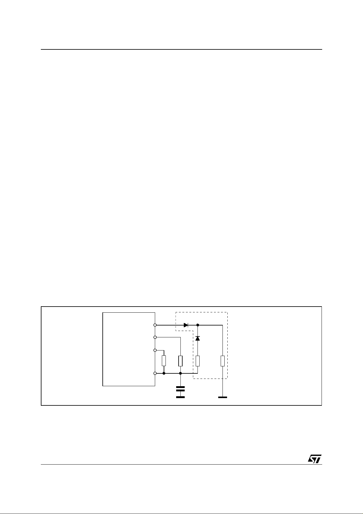
Standby function improvement
To realize the aforementioned function, the osc illator frequency needs to be dependent on c onverter's load conditions - the lower the load, the lower the frequency and vice versa - and only when this is useful, that is at light
load. This can be done by adding few parts to the oscillator of the L5991, as shown in figure 2.
Assuming a perfect matching of the two dio des (with a common-cathode dual di ode like the BAV70 this is closer
to reality), when V
to ground through R
oscillator frequency dec reased, the low er V
3V D1 isolates R
cuit. R
, RB and CT can be then cal culated as us ual with the formulae gi ven i n [1]; as to the deter minatio n of R
A
and R' please refer to the appendix.
to fSB is 5.59, however this value does not account for the dynamic changes of V
osc
may bounce from one threshold to the other and the switching fre-
COMP
to under- or overshooting.
COMP
with a given fSB. The lower limit
osc
, because of
osc
an fSB as low as possible would be required to meet the latest design targets
osc
falls below 3V (oscillator's peak voltage) some of the current that charges CT is diverted
COMP
, D1 an R'. In this way the rate of rise of the voltage across CT is slowed down and the
C
and the oscillator frequency will be either f
C
the lower the frequency. Instead, when V
COMP
or fSB, like in the standard L5991 oscillator cir-
osc
is greater than
COMP
COMP
osc
C
Figure 2. Oscillator modification to improve Standby function
additional parts
D2
D1, D2
D1
B
A
R
R
C
C
R
R'
T
2 x 1N4148
or
1 x BAV70
L5991
6COMP
16 S_BY
Vref4
2
RCT
D2 compensates for the temperature shift of the forward voltage drop VF of D1. Considering that the current
flowing through the diodes is in the hundre d µA or less, D1 and D2 dissip ate negligibl e power and only ambient
temperature affects their V
where R
comes into play will depend on ambient temperature. In real-world operation, considering also that
C
. Assuming D1 and D2 match perfectly, neither oscillator frequency nor the point
F
D1 and D2 do not usually carry the same current, a minimum temperature effect can be observed.
2/18
Page 3

AN1537 APPLICATION NOTE
The "frequency foldback" provided by the additional circuit starts in the neighborhood of V
little before that the high-to-low frequency shift takes place. After the shift, V
switching frequency will be close or exactly equal to f
, depending on the f
SB
will be higher and then the
COMP
to fSB ratio.
osc
= 3V, that is a
COMP
In applications where the switching frequency needs not be tightly fixed for some specific reason there is no
major drawback to thi s technique. The only point to take car e of is that the osc illator f reque ncy be in the audi ble
range only when the peak current is so low that no sound may come from the transformer, even when it is made
with normal const ruction tec hniques. Thi s can be obtained simpl y by choosing f
(e.g. f
> 30kHz seems to be a good rule of thumb).
SB
well above the audible range
SB
The benefits, on the contrary, are considerable:
1) Very low switching frequencies are po ssible which, as already stated, will allow treating the power
throughput as much efficiently as possible: MOSFET's capacitive losses, gate drive consumption and
other parasitic losses will be minimized. See [2] for more details on them.
2) Since the additional com ponents will be c oncerned with taking the os cillator frequency to v ery low
values, the standby frequency
fSB can be kept relatively high, thus reducing the abrupt frequency shift
and eliminating the need for a slow feedback to prevent frequency instability. As already said, keeping f
high has the positive side-effect of eliminating audible noise issues.
SB
3) As a result of the faster dynamic response, start-up under no-load conditions is possible even with a
minimum pre-load on the ou tput. The d ummy load represent ed by t he feedbac k net work, as we ll as
bleeders, if used, can be minimized. The limit to the dummy load reduction is given by the collapse
that the voltage delivered by the self-supply winding experiences with no load, which must not pull
the supply voltage of the L5991 below the UVLO threshold.
To evaluate how much this function modification improves converter's performance at light or no load, the 45W
wide-range mains AC-DC adapter illustrated in [3] and the 80W power-factor-corrected AC-DC adapter described in [4] will be optimized following the guidelines revealed by the above considerations. The "European
Code of Conduct on Efficiency of External Power Supplies", ECC in short, whose limits are summarized in table
1, will be assumed as the reference.
Table 1. Limits envisaged by European Code of Conduct on Efficiency of External Power Supplies
Max. no-load Power Consumption
Rated Input Power
≥ 0.3W and < 15W 1.0W 0.75W 0.30W
≥ 15W and < 50W 1.0W 0.75W 0.50W
≥ 50W and < 75W 1.0W 0.75W 0.75W
Phase 1
01.01.2001
Phase 2
01.01.2003
Phase 3
01.01.2005
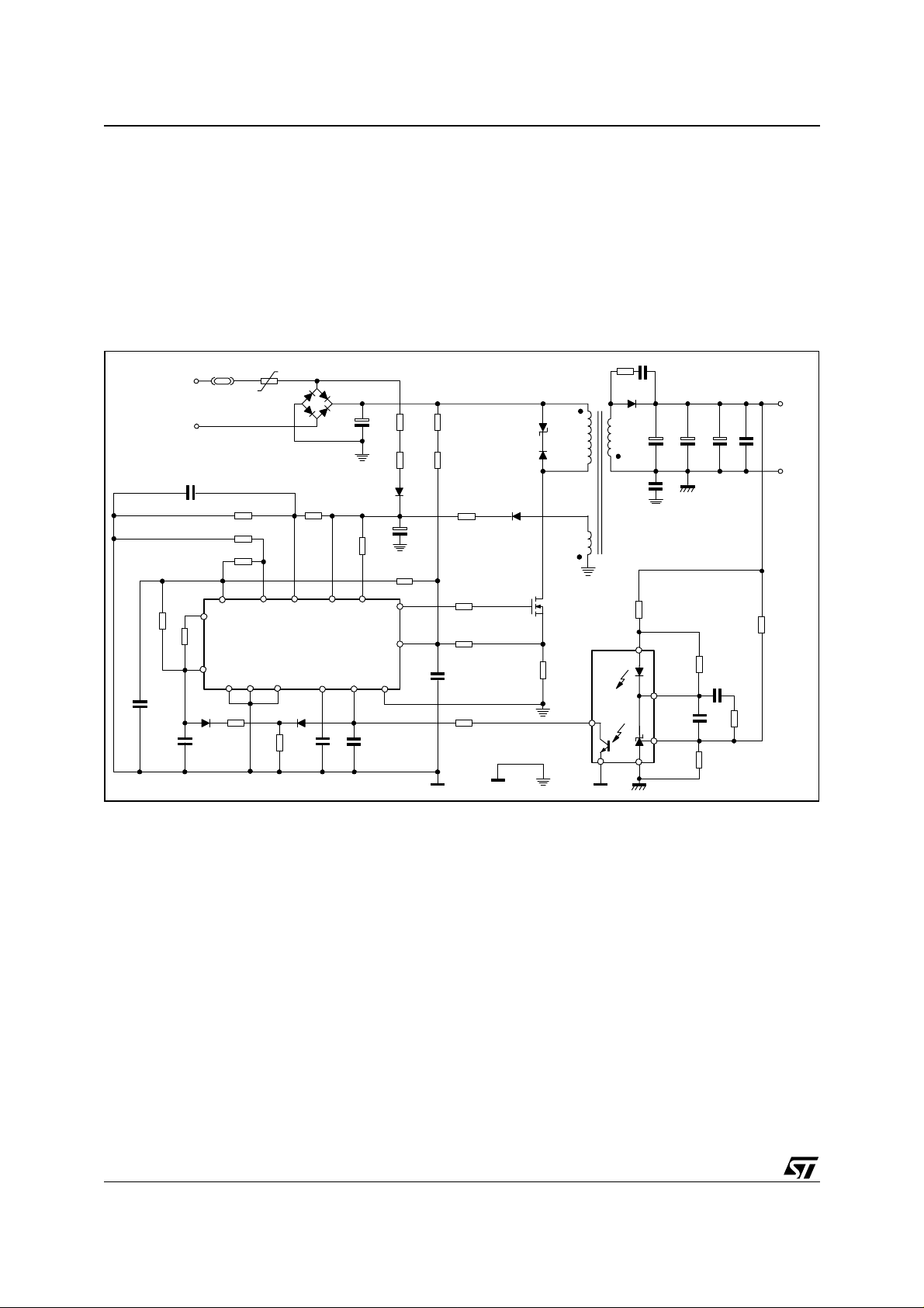
Optimization of a 45W, wide-range mains AC-DC adapter
For reader's convenience, table 2 summarizes the electrical spec of the adapter under consideration. Please
refer to [3] for a detailed description and full evaluation data.
Table 2. 45W, wide-range mains AC-DC adapter: electrical specification of the original design
Input Voltage Range (V
Mains Frequency (f
Maximum Output Power (P
Output
Normal Operation Switching Frequency (f
Light Load Switching Frequency (f
Full-load Efficiency (@ Pout =45W, Vin = 88÷264Vac) > 80%
Maximum no-load Input Power (Vin = 88÷264Vac) < 1W
) 88 to 264 Vac
in
) 50/60Hz
L
) 45W
out
Vout = 18V ± 3%
Iout = 2.5A max.
Full load ripple ≤ 2% pk-pk
) 70kHz typ.
osc
) 18kHz typ.
SB
3/18
Page 4
AN1537 APPLICATION NOTE
Since the full-load input power is greater than 50W, this adapter belongs to the third bracket envisaged by the
ECC. Its no load consumption is 0.9W @264Vac and 0.7W @220Vac then it meets Phase 1 limit (1W) and is
close to that of Phase 2 and 3 (0.75W) with almost no margin.
Although the ECC specifies that the compliance test be done at the nominal voltage 230 Vac, in the pre-compliance test it is quite usual to refer to the consumption at 264 Vac, to account for production spread. With this
criterion the adapter cannot be considered compliant with Phase 2 or 3 limits.
The target of the optimization is then to make the adapter ECC-compliant in the above menti oned sense. Figure
3 shows the electrical schematic of the converter with the added and modified components highlighted. Only
these changes will be discussed.
Figure 3. 45W AC-DC adapter: electrical schematic of the modified circuit
12 k
R12
100 nF
ΩΩΩΩ
C4
C3 100 nF
R13
12 k
88 to 264
ST-BY
ΩΩΩΩ
F1 T2A250V
Vac
R5 47 k
R8 22 k
R9 27 k
VREF
43
16
2
15
RCT
DC-LIM SGND
D6 1N4148
Rc
C5
5.9 k
3.3 nF
12
ΩΩΩΩ
NTC1 N.A.
Ω
ΩΩΩΩ
ΩΩΩΩ
DCC
R'
8.2 k
ΩΩΩΩ
L5991
5
VFB
D7 1N4148
IC1
C6
56 nF
330 k
BD1
DF04M
C1
100 µF
400 V
R6
Ω
R10
Ω
22
814
9
6
7
SS
COMP
1N4148
VCVCCDIS
C7
3.3 nF
D3
10
13
11
56 k
56 k
R23 N.A.
OUT
ISEN
PGND
R1
R2
47 µF
25 V
R3
Ω
Ω
2.2 M
R4
Ω
Ω
2.2 M
R7 1
C2
R11
Ω
10
R14
1 kΩ
C8
100 pF
R16 100
D1
BZW06-154
D2
STTA106
ΩΩΩΩ
D4 1N4148
STP7NB60
Ω
R15
0.47 Ω
1/2 W
Q1
R22
N.A.
T1
N1 N2
N3
R17
4.3 k
IC2
PC905
7
6
D5
BYW29-200
C9
330 µF
25 V
C12
4.7 nF
2kV
Ω
3
C17
N.A.
18V/2.5A
C10
C11
330 µF
25 V
C14
8.2 nF
R21
3.16 k
C15
220 nF
ΩΩΩΩ
20 k
R18
180 k
ΩΩΩΩ
R20
GND
ΩΩΩΩ
330 µF
25 V
1
R19
N.A.
2
C13
N.A.
4
1) The oscillator has been modified to maintain the same frequency under normal operation (70kHz) at
full load and have a standby frequency equal to half the normal frequency (35kHz). The oscillator frequency with no-load will be 5kHz. Further details on the calculations can be found in the appendix.
2) The dummy load represented by the feed back components o n the sec ondary side (170mW in the
original design) has been reduced at 40mW: R21 has been increas ed from 348 Ω to 3.16kΩ and,
consequently, R18 from 2.2 to 20kΩ to maintain the same regulated output voltage. This reduces the
current consumption of the divide r from 7. 2 to 0.8 mA. Additionally, R1 9 wh ich was t o provide 1 mA
extra bias current to the reference of the PC905, has been taken out since it was not strictly necessary.
3) The frequency compens ation of the voltage c ont rol loop (C7 , C14, R20) has been modi fied so as to
get a larger bandwidth - it has been almost doubled - and then a faster response. The main purpose
of that is to allow a correct start-up of t he converter even with no l oad, whereas a slow feedback (basically, a large C14) causes the system to try continuously to restart under these conditions.
4) R7 has been decreased from 4.7 to 1 Ω, to prevent the supply voltage of the L5991 from going below
the UVLO threshold with no load. To help this, the total consum ption of the I C has been reduc ed by
0.3 mA by increasing R8 and R9 (from 5.6 to 22k Ω and from 6.8 to 27kΩ, respectively). Although
with this change the voltage generated at full load is higher, it is still below the OVP threshold, set by
R5 and R6, with a safe margin.
These modifications are summarized in table 3.
4/18
Page 5
AN1537 APPLICATION NOTE
Table 3. 45W, wide-range mains AC-DC adapter: list of modifications to the original design
Part Original value New Value Part Original value New Value
R7 4.7Ω 1Ω R20 5.6kΩ 180kΩ
R8 5.6kΩ 22kΩ R21 348Ω 3.16kΩ
R19 6.8kΩ 27kΩ R
C
R12 24kΩ 12kΩ R’ --- 8.2kΩ
R13 8.2kΩ 12kΩ C7 220pF 3.3nF
R18 2.2kΩ 20kΩ C14 470nF 4.7nF
R19 1.2kΩ --- D6, D7 --- 1N414 8
45W AC-DC adapter: evaluation results
The following diagrams compare the performance of the original design ("standard standby") with that of the
modified one ("improved standby"). For reference, it has also been measured the input consumption after replacing the start-up circuit made up of R1, R2 and D3 with an active start-up circuit (see fig. 12).
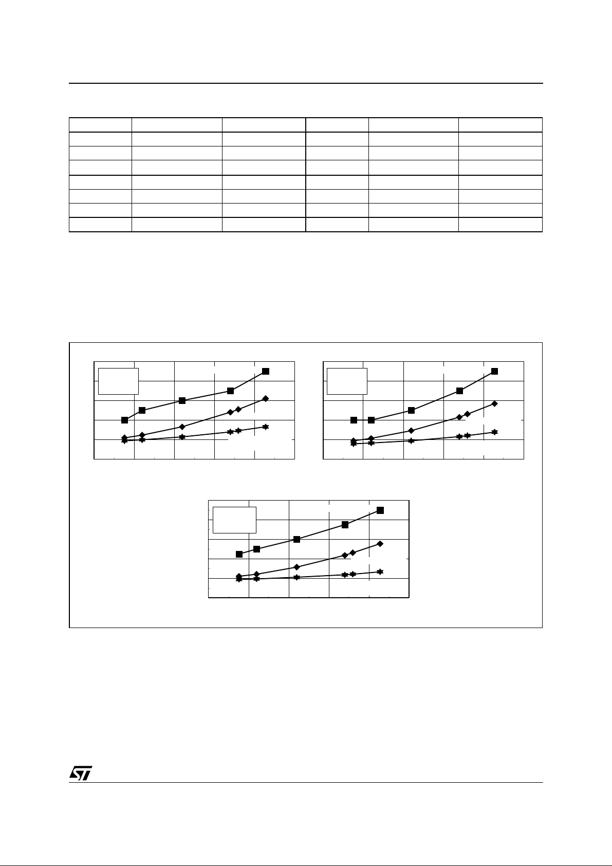
To be noted in figure 4, the no-load consumption is < 0.6W @ 264Vac, then the adapter under test meets the
ECC limits, Phase 3 (< 0.75W @230Vac) with some margin even without the use of an active start-up circuit.
Figure 4. 45W AC-DC adapter: light load input consumption comparison
Pin [ W]
1.6
1.4
1.2
1
Pout = 0.5 W
fsw = 16 kHz
Tamb= 25 °C
standard standby
improved standby
Pin [W]
1.4
1.2
1
0.8
Pout = 0.3 W
fsw = 13 kHz
Tamb= 25 °C
--- 5.9kΩ
standard standby
improved standby
0.8
0.6
50 100 150 200 250 300
(*) refer to the circuit shown in
the schematic of figure 12
Vin [Vac]
Pin [W]
1
0.8
0.6
0.4
0.2
0
improved standby
with active start-up (*)
Pout = 0 W
fsw = 5 kHz
Tamb= 25 °C
50 100 150 200 250 300
(*) refer to the circuit shown in
the schematic of figure 12
0.6
0.4
50 100 150 200 250 300
(*) refer to the circuit shown in
the schematic of figure 12
standard standby
improved standby
improved standby
wit h act ive start-u p (*)
Vin [Vac]
Vin [Vac]
improved standby
with active start-up (*)
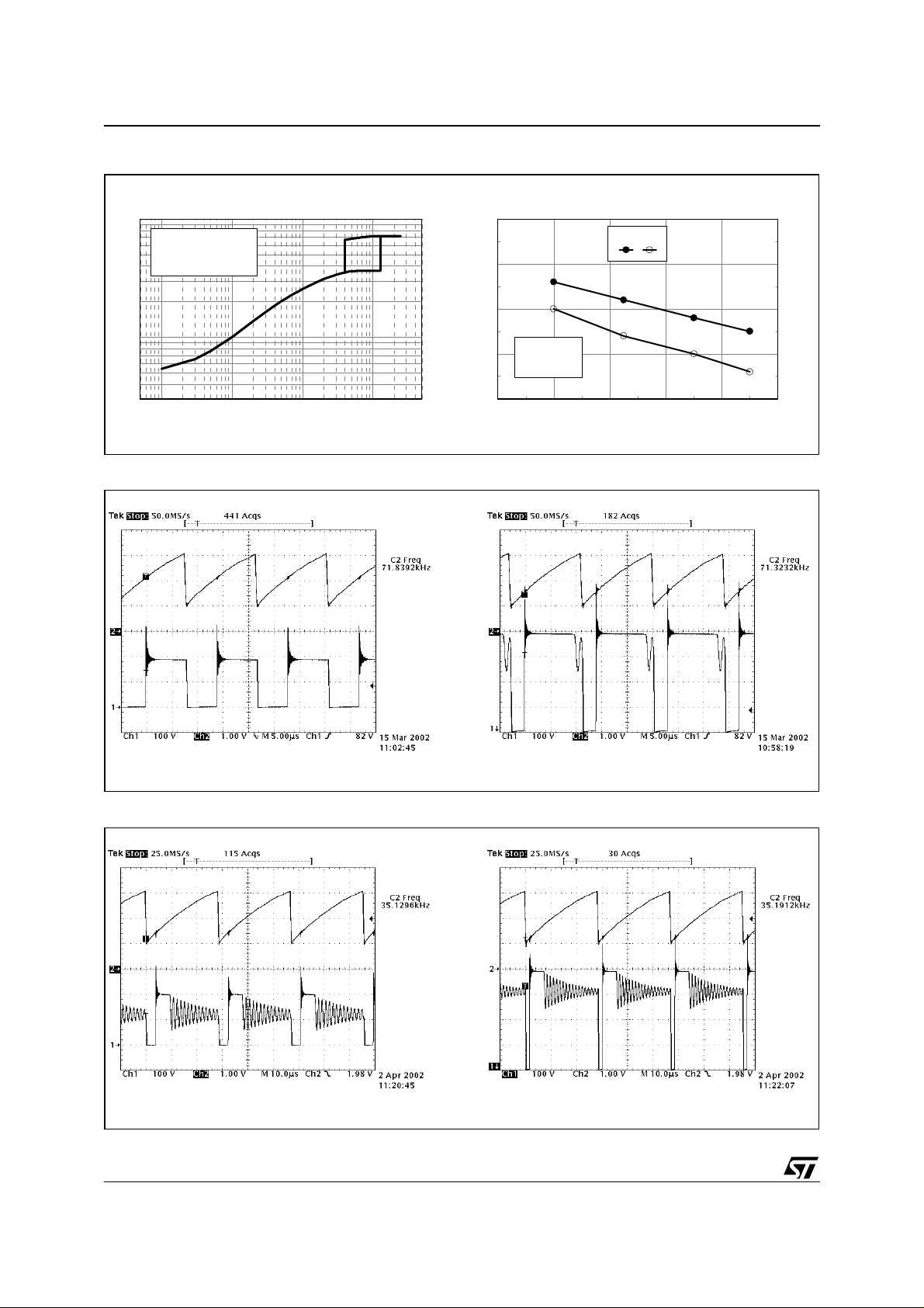
The diagram on the left in figure 5 shows the relationship between output current and switching frequency obtained with the modified oscillator. The oscillator frequency is not much affected by the input voltage, as shown
also by the oscilloscope diagrams of figures 6 to 10: the internal propagation delay of the current sense pin is
compensated by R3 and R 4, then the changes of V
(and, consequently, fsw) with the input voltage are neg-
COMP
ligible.
The diagram on the right in figure 5 illustr ates the effect of temperature on both the os cilla tor frequenc y and the
no-load input consumption (@264Vac) in the temperature range 0-70°C: the variation is very limited.
5/18
Page 6
AN1537 APPLICATION NOTE
Figure 5. 45W AC-DC adapter:
fsw
vs.
I
out
(left);
Pin
fsw [kHz]
100
50
Tamb = 25 °C
Vin = 11 0 Vac, 23 0 Vac
30
20
10
5
3
0.001 0.01 0.1 1
Iout [A]
Figure 6. 45W AC-DC adapter: waveforms @ P
RCT (pin 2 of L5991)
(@
P
= 0) and
out
fsw vs. ambient temperature (right)
fsw [kHz] Pin [W]
7
fsw Pin
6
5
Pout = 0 W
4
Vin = 264 Vac
3
-20 0 20 40 60 80
Tamb[°C]
= 45W
out
RCT (pin 2 of L5991)
0.58
0.57
0.56
0.55
0.54
Q1 Drain
Vin = 110 Vac, Pout = 45W
Figure 7. 45W AC-DC adapter: waveforms
RCT (pin 2 of L5991)
Q1 Drain
@
Q1 Drain
Vin = 220 Vac, Pout = 45W
P
= 7W, just after the abrupt frequency shift
out
RCT (pin 2 of L5991)
Q1 Drain
6/18
Vin = 110 Vac, Pout = 7W
Vin = 220 Vac, Pout = 7W
Page 7

AN1537 APPLICATION NOTE
Figure 8. 45W AC-DC adapter: waveforms @ P
RCT (pin 2 of L5991)
Q1 Drain
Vin = 110 Vac, Pout = 0.5W
@
Figure 9. 45W AC-DC adapter: waveforms
RCT (pin 2 of L5991)
P
out
out
= 0.5W
RCT (pin 2 of L5991)
Q1 Drain
Vin = 220 Vac, Pout = 0.5W
= 0.3W
RCT (pin 2 of L5991)
Q1 Drain
Vin = 110 Va c, Pout = 0.3W
Figure 10. 45W AC-DC adapter: waveforms
RCT (pin 2 of L5991)
Q1 Drain
@
P
out
= 0W
Q1 Drain
Vin = 220 Vac, Pout = 0.3W
RCT (pin 2 of L5991)
Q1 Drain
Vin = 110 Vac, Pout = 0W
Vin = 220 Vac, Pout = 0W
7/18
Page 8

AN1537 APPLICATION NOTE
Figure 11. 45W AC-DC adapter: load transient 0.1 ⇔ 2 .5A @ 220Va c
Iout
Vout
COMP (pin 6 of L5991)
Optimization of a 80W AC-DC adapter with PFC
Table 4 summarizes the items of the electrical spec of this adapter more relevant to this context. Please refer
to [4] for full electrical spec and evaluation data, as well as for a detailed description.
Table 4. 80W AC-DC adapter with PFC: electrical specification of the original design
Input Voltage Range (Vin) 90 to 265Vac
Mains Frequency (fL) 50/60Hz
Maximum Output Power (P
Output V
Line and Load regulation < 1%
Switching Frequency (Flyback, @ P
Switching Frequency (Flyback, @ P
Target Overall Efficiency (@ P
Maximum No-load Input Power (Vin = 90 ÷265Vac) < 1W
) 80W
outmax
= 80W) 65kHz
out
= 0W) 20kHz
out
= 80W, Vin = 90÷265Vac) η > 75%
out
= 18Vdc ± 2%
out
I
= 0 to 4.5A
out
V
≤ 1%
ripple
The full-load input power is greater than 100W, then this adapter is actually out of the scope of the ECC. Its no
load consumption (0.9W @265Vac, 0.7W @220 Vac), however, is within the Phase 1 limit (1W) and not far
from that of Phase 2 and 3 (0.75W @230 Vac) for the highest power bracket.
Again, the target of the optimization is to meet Phase 3 limit @Vin = 264 Vac. Figure 12 shows the electrical
schematic with the added and modified components highlighted. Only these changes, which track those made
in the previously considered design plus those related to the PFC stage, will be discussed
8/18
Page 9

AN1537 APPLICATION NOTE
Figure 12. 80W AC-DC adapter with PFC: electrical schematic of the modified circuit
D1 STTA106
T1A
F
µ
47
F
µ
100
GND_OUT
C27
C6
C24
C22
C21
C20
C19
D12 A,B,C
3 x 1.5KE68
25V
25V
D6
T2B
T2A
Z18
100nF
F
µ
680
F
µ
680
F
µ
680
F
µ
680
F
µ
680
ZR2
25V
25V
25V
25V
25V
D7
R26 22
MUR1100
C26
R39
C
V
CC
V
4.7nF
10M
Q2
R23 22
OUT
STP7NB80
R24 1K
Isen
101315
IC2
DC-LIM
20K
R31
R29
3.16K
33K
R33
C25
3.3n
C16
PC817A
1N4148
N.A.
VR1
TL431C
C15
220pF
R36
5.6K
C13
C11
C10
C9
3.3nF
10nF
3.3nF
100nF
TR5
BC557
C
R
7.5K
D13
1N4148
N.A.
R30
R32
4.3K
1
2
OC1
4
3
R25A,B
0.56 // 0.56
PGND
11
651272416
D14
27K
R37
F
µ
C14
4.7
L5991A
R15 15K
R16 11K
+18V / 4.5A
µ
L1 2.2
F
µ
C28
450V
100
22K
1.5M +
1.5M +
R7A,B
33 nF
C30
F
µ
C8 1
R2
T1B
R3A, B
D3
D2
400V
+
1.5M
68K
1.5M
499K
R7C
R4 33
7
IC1
52 1
F
µ
C1
630V
0.22
D5
D4
F
µ
C3
630V
0.68
R6A
C23 N.A.
Q1
R5A,B
STP9NB50
0.56 // 0.56
4
6
F
µ
25V
C29
L6561
3
10
8
BYW51-200
D11
R27 N.A.
T2C
R28 1
C7
10nF
R1
22K
C4
4.7nF
R38 47
R22A, B
C17
C18
D10 1N4148 D9 BAV19
10K +
10K
Q3
STD1NB50
R19
100K
C12 100nF
R18 330K
R17 47K
DIS
14 8 9
3
6.8K
6.8K
ST-BY VREF RCT SS SGND VFB COMP
D8
1N4148
DCC
R13
R14
TR4
10M +
C5
LF2-A
ZR1
SI0300
F
µ
C2
0.47
LF1-A
F1 T4A
LF1-B LF2-B
NTC1 10
to
90 Vac
264Vac
4.7nF
10M
R21A, B
BC547
R20 100K
R11
27K
TR3
BC557
R12
R10
100K
R9
R8
150K
150K
47K
TR2
BC547
TR1
BC547
9/18
Page 10

AN1537 APPLICATION NOTE
1 The oscillator of the L5991 has been mod ified to ma intain t he sam e f requency unde r n ormal opera-
tion (65kHz) at full load and have a standby freq uenc y of 36kHz. Also in this case the oscillator frequency with no-load is chosen 5kHz. Further details on the calculations can be found in the appendix.
2 Again, the dummy load represented by the feedback components on the secondary side has been
reduced at about 40mW (see the same point of the previous design).
3 The frequency compensation of the voltage control loo p (C7, C14, R20) has been modified so as to
double the bandwidth and get a faster response (especially useful at start-up).
4
R28 has been decreased from 3.3 to 1Ω, to prevent the supply voltage of the L5991A from going below
the UVLO threshold with no load, while not exceeding the rating of both the L5991A and the L6561.
5 The multiplier bias resistors (R3A = R3B = 680k Ω and R1 = 10 kΩ) of the L6561 con sume 103m W
@264 Vac, then their value has been more than doubled (R3A = R3B = 1.5M Ω and R1 = 22kΩ). In
this way their maximum consumption is reduced at 46mW @264 Vac.
6 The out put di vider of th e P FC p re-regulat or (R7A = R7B = 499k Ω and R1 = 6.34kΩ ) gives origin to
a consumption of 140mW @264 Vac. With the aim of reducing the consumption at 40mW maximum,
while not degrading the dynam ic OVP function, the feed back network has bee n modified as shown
in figure 13. The cap ac itor bypas ses the t wo 1. 5M Ω resistors during out put v oltage ov ershoot s, resulting in a only slightly higher OV P threshold, as compa red to the original one. The pos itive sideeffect is an improvement of the transient response of the PFC pre-regulator. The components for the
frequency compensation of the error amplifier of the L6561 have been changed consequ ent ly.
The modifications are summarized in table 5.
Figure 13. Modified PFC pre-regulator's feedback and frequency compensation network
PFC out
C30
33 nF
400V
C8 1µF
2
R7A
1.5M
R7B
1.5M
R7C
499K
R6A
22K
L6561
Table 5. 80W AC-DC adapter with PFC: list of modifications to the original design
Part Original value New Value Part Original value New Value
R1 10kΩ 22kΩ R31 2.2kΩ 20kΩ
R3A, R3B 680kΩ 1.5MΩ R33 13kΩ 33kΩ
R6A 6.34kΩ 22kΩ R34 510kΩ ---
R7A, R7B 499kΩ 1.5MΩ R35 2.2kΩ shorted
R7C --- 499kΩ R36 10kΩ 5.6kΩ
R15 10kΩ 15kΩ R
R16 22kΩ 11kΩ C13 15nF 3.3nF
R28 3.3Ω 1Ω C25 330nF 3.3nF
R29 348Ω 3.16kΩ C30 --- 33nF / 400V
R30 1.2kΩ --- D13, D14 --- 1N4148
C
--- 7.5kΩ
10/18
Page 11

AN1537 APPLICATION NOTE
80W AC-DC adapter with PFC: evaluation results
The following diagrams compare the performance of the original design ("standard standby") with that of the
modified one ("improved standby").
To be noted in figure 14, the no-load consumption is slightly less than 0.5W @ 264Vac, then the modified 80W
adapter now meets the ECC limits, Phase 3 for the 15-50W bracket (< 0.5W @230Vac).
Figure 14. 80W AC-DC adapter with PFC: light load input consumption comparison
Pin [W]
1,5
1,4
Pout = 0.5 W
Tamb= 25 °C
1,3
1,2
1,1
1
0,9
0,8
50 100 150 200 250 300
Vin [Vac]
standard standby
improved standby
Pin [W]
1
Pout = 0 W
Tamb= 25 °C
0,8
0,6
0,4
0,2
50 100 150 200 250 300
Pin [W]
1,4
Pout = 0.3 W
1,2
Tam b= 2 5 °C
1
0,8
0,6
0,4
50 100 150 200 250 300
standard standby
improved standby
Vin [Vac]
standard standby
improved standby
Vin [Vac]
Figure 15. 80W AC-DC adapter with PFC: f
fsw [kHz]
100
Tamb = 25 °C
50
30
20
Vin = 110 Vac
10
5
3
Vin = 230 Vac
0.001 0.01 0.1 1
Iout [A]
sw
vs. I
5
(left); fsw vs. Vin (right)
out
fsw [kHz]
18
16
14
12
10
8
6
4
2
50 100 150 200 250 300
Vin [Vac]
Tamb= 25 °C
Pout = 0.5W
Pout = 0.3W
Pout = 0W
11/18
Page 12

AN1537 APPLICATION NOTE
Figure 16. 80W AC-DC adapter with PFC: Pin (@ P
fsw [kHz] Pin [W]
12
fsw Pin
10
8
Pout = 0 W
Vin = 110 Vac
6
4
2
-20 0 20 40 60 80
Tamb[°C]
0.34
0.32
0.3
0.28
0.26
0.24
= 0) and fsw vs. ambient temperature
out
fsw [kHz] Pin [W]
12
fsw Pin
10
8
6
4
2
-20 0 20 40 60 80
Tamb[°C]
Pout = 0 W
Vin = 230 Vac
0.46
0.44
0.42
0.4
0.38
0.36
The diagrams in figure 15 illustrate the relationship between output current, input voltage and switching frequency obtained with the modified oscillator. Unlike the previously considered design, in this case the internal
propagation delay of the c urrent sense pin is not compe nsated, then V
changes slightly with the input volt-
COMP
age and then there is a variation of the oscillator frequency.
The diagrams of figure 16 illustrate the very limited temperature effect on both the oscillator frequency and the
no-load input consumption at both nominal voltages in the temperature range 0-70 °C.
Figure 17. 80W AC-DC adapter with PFC, flyback section: waveforms @ P
= 80W
out
RCT (pin 2 of L5991)
Q2 Drain
Figure 18. 80W AC-DC adapter with PFC, flyback section: waveforms @ P
RCT (pin 2 of L5991)
Q1 Drain
RCT (pin 2 of L5991)
Q1 Drain
= 30W
out
12/18
Vin = 110 Vac, Pout = 30W Vin = 230 Vac, Pout = 30W
Page 13

AN1537 APPLICATION NOTE
Figure 19. 80W AC-DC adapter with PFC, flyback section: waveforms @ P
RCT (pin 2 of L5991)RCT (pin 2 of L5991)
Q2 Drain
Q2 Drain
Vin = 110 Vac, Pout = 0.5W Vin = 230 Vac, Pout = 0.5W
Figure 20. 80W AC-DC adapter with PFC, flyback section: waveforms @ P
RCT (pin 2 of L5991)
RCT (pin 2 of L5991)
= 0.5W
out
= 0.3W
out
Q2 Drain
Q2 Drain
Vin = 110 Vac, Pout = 0.3W
Vin = 230 Vac, Pout = 0.3W
Figure 21. 80W AC-DC adapter with PFC, flyback section: waveforms @ P
RCT (pin 2 of L5991)RCT (pin 2 of L5991)
Q2 Drain
Q2 Drain
out
= 0W
Vin = 110 Vac, Pout = 0W Vin = 230 Vac, Pout = 0W
13/18
Page 14

AN1537 APPLICATION NOTE
Figure 22. 80W AC-DC adapter with PFC, flyback section: load transient 0.1 ⇔ 4. 5A @ 220V ac
Iout
Vout
COMP (pin 6 of L5991)
Conclusions
A simple modification of the oscillator allows optimizing L5991-based converters to achieve a considerable decrease of the no-load consumption. This has been proved in a 45W AC-DC adapter and in an 80W power-factorcorrected adapter, w here the opti mization her e proposed has brought a reduction of the no-load in put consumption up to 400mW at high line.
This is the result of concurrent improvements. The modification to the oscillator allows very low switching frequency under no-load condi tions without a large f
headroom for overshoots and undershoots, so that it has been possible to enlarge the bandwidth of the control
loop without any frequency instability. In turn, the faster response due to the larger bandwidth has allowed the
reduction of the dummy load on the output, without compromising correct start-up when the adapter is unloaded.
The lower residual load and the loss reduction due to the very low oscillator frequency, results in a dramatic
decrease of the power absorbed from the mains at no load.
to fSB ratio. The resulting lower V
osc
jump provides more
COMP
REFERENCES
[1] "L5991/L5991A Primary Controller with Standby" Datasheet
[2] "Minimize Power Losses of Lightly Loaded Flyback Converters with the L5991 PWM Controller" (AN1049)
[3] "45W AC-DC Adapter with Standby Function" (AN1134)
[4] "80W Power-factor-corrected AC-DC Adapter with Standby Using the L6561 and the L5991A" (AN1440)
14/18
Page 15

AN1537 APPLICATION NOTE
APPENDIX
How to calculate R
As previously said in the section
timing components C
only the calculation of R
To this end it is necessary to c onsider fi r st the timing equations that gov ern the operati on of the oscillator. Refer
to figure A1 for the equivalent circuit and the relevant waveform, which assume that D1 and D2 match.
Figure A1. Equivalent circuit for oscillator calculations (left) and theoretical V(RCT) waveform (right)
and R'.
C
"Standby function improvement"
, RA, RB because RC is disconnected by the series diode D1 when V
T
C
6COMP
to get a given f
, as well as that of R' needs to be taken into consideration.
min
3
, there is no change for the calculation of the
1
f
SB
COMP
> 3V. Then
SW
L5991
open if V(RCT)> V
SW
{
closed if V (RCT)> V
Vref4
A
R
2
RCT
COMP
COMP
C
R
V(RCT)
T
C
As long as the oscillator voltage V(RCT) is less then V
2.5
2
1.5
COMP
openSWclosed
SW
A
T
τ
· C
= R
1
A
τ
' = (R
1
T
// RC) · C
T
t
, D1 is reverse-biased (SW is open) and only R
VCOMP
Tsw0
contributes to the time constant τ; moreover, the asymptote of the exponential curve is the reference voltage
V
(5V). When V(RCT) equals and exceeds V
REF
parallel to R
Note that the new time constant
to determine the time constant τ' and the asymptote will be changed to:
A
V
REF
τ
' is shorter, then it will be the lower asymptote the responsible for getting a
R
C
--------------------- -
RARC+
, D1 is forward-biased (SW is closed), then RC goes in
COMP
R
A
COMP
--------------------- -
RARC+
V
<+
REF
V
longer oscillator period. The complete equation describing the oscillator is then
t
--–
τ
–
tT
≤+
1
R
A
----------------------
RARC+
–
V
REFVV
----------------------------------------
ln τ
–
V
REFVCOMP
R
C
----------------------
RARC+
V
–()– e
REFVCOMP
4
-----------------------------
ln==
5V
–
COMP
tT1–
--------------–
τ'
tT
>+
1
(A1)
V RCT()
where:
=
V
V
V
REF
V
REFVV
R
C
----------------------
RARC+
–()1e
V
COMP
τ
T
1
A
is the time when V(RCT) = V
(1V) and the time constants
To find a simple formula to calc ulate R
will be neglected and it is possible to write:
V
, (A2)
pk
where V
T
<< Tsw it will be also τ' << Tsw and the exponential term in (A2) can be neglected. Then (A2) becomes:
1
is the oscillator peak voltage (3V) and V
pk
V
REF
----------------------
RARC+
and RC comes into play (i.e. SW is closed), VV is the oscillator val ley v oltage
COMP
τ
and τ' are defined as shown in figure A1.
some simplific ations are necess ary. U suall y T1 << Tsw = 1/f
C
T
SW
R
C
V
COMP
R
----------------------
0
RARC+
A
COMP
R
C
----------------------
–+=
RARC+
the value of V
0
V
–()e
REFVCOMP
under no-load conditions. But, if
COMP
-----------–
τ'
0
min
, then T
15/18
1
Page 16

AN1537 APPLICATION NOTE
that, solved for RC, yields:
R
C
--------------------- -
V
R
C
V
pk
RA=
REF
V
–
pkVCOMP
--------------------------------------
V
REFVpk
RARC+
–
V
+=
COMP
3V
0
=
–
------------------------------ -
R
A
--------------------- -
0
RARC+
COMP
2
R
A
0
. (A3)
The maximum value for R' can be calculated by imposing that D2 be always forward-biased, that is its current
never fall to zero, with V
COMP
= V
. The current flowing through D2 is:
COMP
0
V
I
---------------------------------- - I
D2
COMP
R'
VF–
0
–=
,
D1
while the maximum current flowing through D1 is:
Then, imposing I
Since I
and ID2 are typically in the hundred µA, with good approximation it is possible to assume VF = 0.5V
D1
VpkVFV
I
D1x
> 0 with ID1 = I
D2
-------------------------------------------------------------------- -
R'R
COMP
R
C
and solving for R', it is possi ble to obtain:
D1x
V
COMP
--------------------------------------
< R
C
V
–
pkVCOMP
VF–()––
0
VF–
0
=
0
–
V
pkVCOMP
------------------------------------- -
R
C
V
COMP
3V
–
COMP
0
---------------------------------- -
C
0
VF–
. (A4)
0
–
3V
COMP
R
0
.
C
------------------------------ -===
@ 25°C in (A4). Worst-case scenario is at minimum operating temperature: -2.5 mV/°C drift can be considered
to take this into account.
The point is now to calculate the value of V
. In [2] it is shown that in L5991-based flyback converters the
0
COMP
following relationships holds true:
2P
V
COMP
1.4 3 R s
--------------
fswL
where Rs is the sense resistor (R15 in figure 3, R25 in figure 12), P
primary inductance, V
sense pin (200 ns typ.) and V
In case the offset V
the DC input voltage to the converter , T
in
is chosen equal to
o
a DC voltage offset that can be applied to the current sense pin.
o
V
------- -
Rs
L
V
in
in
------- -
T
–
delay
L
p
p
delay
in
T
p
delay
,
V
++=
, (A5)
o
the input power to the transformer, Lp its
in
the internal propagation del ay of the current
the effect of the propagation delay is compensated and V
will no longer depend on the input voltage Vin.
COMP
That is the case of the 45W adapter, where the job is done by R3 and R4 along with R14. For the 80W adapter
there is no compensation (V
frequency when R
Figure A2. V
16/18
is active) on Vin. This is confirmed by the experimental results.
C
voltage under no-load conditions: 45W adapter (left), 80W adapter (right)
COMP
= 0) then there will be a slight dependence of V
o
45W Adapter 80W Adapter
(and then of the oscillator
COMP
Page 17

AN1537 APPLICATION NOTE
To calculate V
, Pin needs to be estimated considering the power processe d by the transfor mer under no-
0
COMP
load conditions. It is possible to use the following formula:
P
= 1.25(V
in
where I
is the residual output current (through the output divider, through the optocoupler's LED, as well
outres
as any residual dummy load resistor), V
out Ioutres
is the voltage generated by the auxiliary winding that supplies the
aux
L5991 (and the L6561 in the 80W adapter) and I
+ V
the total consumption on this winding (quiescent current of
aux
aux Iaux
) , (A6)
the L5991, of the L6561 too in the 80W adapter, optocoupler's transistor current and the consumption of any
circuit supplied by the reference voltage of the L5991 or dir ectly connected to its supply bus). The coefficient
1.25 stems from an estimated efficiency of 80% that experiments have shown many flyback transformers feature under no-load conditions, almost regardless of their size, parameters and construction.
It is obvious that the estima te of P
tote of the oscil lator waveform that governs the osc illator frequen cy, even some ten mV variation of V
change the frequency considerably. A small error in the assessment of V
R
that gives an f
C
away from the target. This is why it is recommended to use the result of the calculation as
min
is the weak poi nt of thi s des ign proc edure . Since i t is ess entially the as ymp-
in
, then, could lead to a value for
0
COMP
COMP
may
0
a starting point that has to be checked on the bench and, in case, corrected after the experiments. For completeness, it must be said also that under no-load conditions V
is far from being a perfect DC voltage, as
COMP
shown in the diagrams of figure A2.
45W adapter example calculation
With CT = 3.3nF, RA and RB are 12kΩ each. The residual output load is 40mW, the total consumption of the
auxiliary winding is estimated around I
= 10mA, that is 110mW assuming V
aux
≈ 1.25 (0.04 + 0.11) = 0.188W .
P
in
= 11V. Then, using (A6):
aux
V
will be given by (A5), where it is assumed a perfect propagation delay compensation:
COMP
0
V
COMP
1.4 3 0. 47
0
2 0.188⋅
------------------------------------------------⋅+ 2.011V==
3
510
400 10
⋅⋅⋅
6–
.
From (A3):
R
C
From (A4), considering T
R'5.9 10
12 103
= 0°C, then VF = 0.563V:
amb
⋅< 8.638 103⋅=
----------------------- -
⋅ 5.934 103⋅==
3
2
2.011 0.563–
----------------------------------- -
3 2.011–
use standard value 5.9k
use standard value 8.2k
Ω
.
Ω
.
3 2.011–
80W adapter example calculation
With CT = 3.3nF, we get RA =15kΩ and RB = 11kΩ. The residual output load is 40mW, the total estimated consumption of the auxiliary winding is I
V
will be given by (A5):
0
COMP
V
COMP
1.4 3 0. 28
0
= 12mA, that is 120mW assuming V
aux
≈ 1.25 (0.04 + 012) = 0.2W
P
in
⋅+ 1.616V==
20.2⋅
------------------------------------------------
3
510
430 10
⋅⋅⋅
375 200 10
⋅⋅
---------------------------------------- -–
6–
430 10
= 10V. Then, using (A6):
aux
9–
6–
⋅
.
From (A3):
3 1.616–
R
C
From (A4) ), considering T
R'7.5 10
11 103
amb
⋅⋅< 5.706 10
----------------------- -
⋅ 7.612 103⋅==
2
= 0 °C, then VF = 0.563 V:
3 1.616 0.563–
----------------------------------- -
3 1.616–
⋅=
use standard value 7.5k
3
use standard value 5.6k
Ω
Ω
.
17/18
Page 18

AN1537 APPLICATION NOTE
Information furnished is believed to be accurate and reliable. However, STMicroelectronics assumes no responsibility for the consequences
of use of such information nor for any infringement of patents or other rights of third parties which may result from its use. No license is granted
by implic ation or otherwise under any patent or patent r i ght s of STMi croelectr oni cs. Specifications menti oned in thi s publicati on are subj ect
to change without notice. This publication supersedes and replaces all information previously supplied. STMicroelectronics products are not
authorized for use as cri tical components in li f e support dev i ces or systems without express writ t en approval of STMicroel ectronics.
The ST logo is a registered trademark of STMicroelectronics
2003 STMicroelectronics - All Ri ghts Rese rved
Austra lia - Brazil - Canada - Ch i na - F i nl and - France - Germany - Hong Kong - India - Israel - Italy - Japan -Malay si a - Malta - Morocco -
Singap ore - Spain - Sw eden - Switzerland - Uni ted Kingdom - United St ates.
STMicroelectronics GROUP OF COMPANIES
http://www.s t. com
18/18
 Loading...