

Page 1

AN1528
APPLICATION NOTE
ST92F120/F124/150/F250 TESTFLASH
INTRODUCTION
The testflash is a ST reserved flash area that contains device information, flash parameters
and the boot code. This boot code contains the protocol for In-System Programming and the
TM
routines for E3
factory before shipping and cannot be erased or programmed in user mode.
The purpose of this document is to give an sufficiently accurate description of the testflash
content to allow the user to access to the different parameters and routines included in the
testflash.
After an overview of the testflash content, the document describes the different routines that
can be called at any time by the user code. The last part of this document provides guidelines
on the way to handle an E3
initialization and management. The testflash is programmed by ST at the
TM
failure.
1 GLOSSARY AND ACRONYMS
The terms, abbreviations and acronyms used in this document are listed below and described
in alphabetical order.
– CONFxR: CONFiguration x Register
– NVAPR: Non Volatile Access Protection Register
– NVCSSx: NV Complementary Sector Status x
– NVESPx: NV Emulation Status Pointer x
– NVPWDx: Non Volatile PassWorD x
– NVWPR: Non Volatile Write Protection Register
– REDxR: REDundancy x Register
– VCSSx: Volatile Complementary Sector Status x
– VESPx: Volatile Emulation Status Pointer x
Rev. 3.0
AN1528/0105 1/18
1
Page 2

Table of Contents
INTRODUCTION . . . . . . . . . . . . . . . . . . . . . . . . . . . . . . . . . . . . . . . . . . . . . . . . . . . . . . . 1
1 GLOSSARY AND ACRONYMS . . . . . . . . . . . . . . . . . . . . . . . . . . . . . . . . . . . . . . . . . . 1
2 OVERVIEW . . . . . . . . . . . . . . . . . . . . . . . . . . . . . . . . . . . . . . . . . . . . . . . . . . . . . . . . . . 3
2.1 VECTOR TABLE . . . . . . . . . . . . . . . . . . . . . . . . . . . . . . . . . . . . . . . . . . . . . . . . . 4
2.1.1 Device identifier . . . . . . . . . . . . . . . . . . . . . . . . . . . . . . . . . . . . . . . . . . . . . . 4
2.1.2 Testflash code revision . . . . . . . . . . . . . . . . . . . . . . . . . . . . . . . . . . . . . . . . 4
2.2 USER OTP AREA . . . . . . . . . . . . . . . . . . . . . . . . . . . . . . . . . . . . . . . . . . . . . . . . 4
2.3 PROTECTIONS . . . . . . . . . . . . . . . . . . . . . . . . . . . . . . . . . . . . . . . . . . . . . . . . . . 5
3 ROUTINES DESCRIPTION . . . . . . . . . . . . . . . . . . . . . . . . . . . . . . . . . . . . . . . . . . . . . 6
3.1 POWER-ON ROUTINE (230020H) . . . . . . . . . . . . . . . . . . . . . . . . . . . . . . . . . . . . 6
3.2 NON MASKABLE INTERRUPT ROUTINE . . . . . . . . . . . . . . . . . . . . . . . . . . . . . 7
3.3 CODE UPDATE ROUTINE: IN-SYSTEM PROGRAMMING . . . . . . . . . . . . . . . . 8
3.4 E3
3.5 E3
TM
INITIALIZATION ROUTINE (230026H) . . . . . . . . . . . . . . . . . . . . . . . . . . . 9
TM
SWAP ERROR ROUTINES . . . . . . . . . . . . . . . . . . . . . . . . . . . . . . . . . . . 11
3.5.1 Find Wrong Pages (230029h) . . . . . . . . . . . . . . . . . . . . . . . . . . . . . . . . . . 11
3.5.2 Find Wrong Bytes (23002Ch) . . . . . . . . . . . . . . . . . . . . . . . . . . . . . . . . . . 12
3.5.3 Complete Aborted Swap (23002Fh) . . . . . . . . . . . . . . . . . . . . . . . . . . . . . 13
TM
3.6 E3
RESET TO DELIVERY STATUS (230032H) . . . . . . . . . . . . . . . . . . . . . . 14
3.7 USER ROUTINE FOR EXTERNAL WATCHDOG REFRESH . . . . . . . . . . . . . . 15
TM
4 E3
FAILURE RECOVERY . . . . . . . . . . . . . . . . . . . . . . . . . . . . . . . . . . . . . . . . . . . 17
4.1 ERASE OR WRITE ERROR: FATAL ERROR . . . . . . . . . . . . . . . . . . . . . . . . . . 17
4.2 SWAP ERROR: NON FATAL ERROR . . . . . . . . . . . . . . . . . . . . . . . . . . . . . . . 17
4.2.1 Generate a reset . . . . . . . . . . . . . . . . . . . . . . . . . . . . . . . . . . . . . . . . . . . . 17
4.2.2 Call the “complete aborted swap phase” routine in testflash. . . . . . . . . . . 17
2/18
1
18
Page 3
ST92F120/F124/150/F250 TESTFLASH
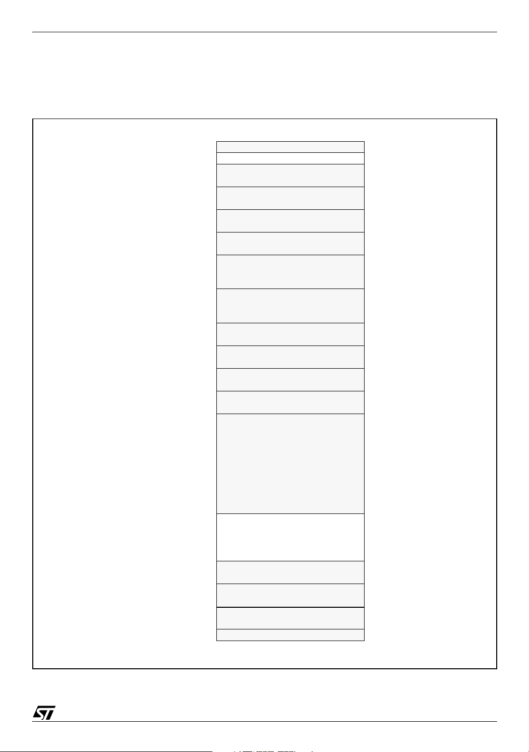
2 OVERVIEW
The structure of the TestFlash content is shown by the following figure:
Figure 1. ST9 TestFlash content
230000h
230020h
230023h
230026h
230029h
23002Ch
23002Fh
230032h
230035h
Vec t o r Table
Powe r-On
routine
Code Update routine
(in-system programming)
SCI Interrupt
routines
E3TM Initialization
TM
E3
Management
routines
E3TM Swap Error:
Find Wrong Pages
E3TM Swap Error:
Find Wrong Bytes in given Page
E3TM Swap Error:
Complete aborted Swap phase
E3TM Reset
to delivery status
230E80h
231E80h
231F78h
231F80h
231FFCh
Not Used
(4 Kbytes)
Reserved for Testing
(248 bytes)
Otp area
124 bytes
Protections
3/18
2
Page 4
ST92F120/F124/150/F250 TESTFLASH
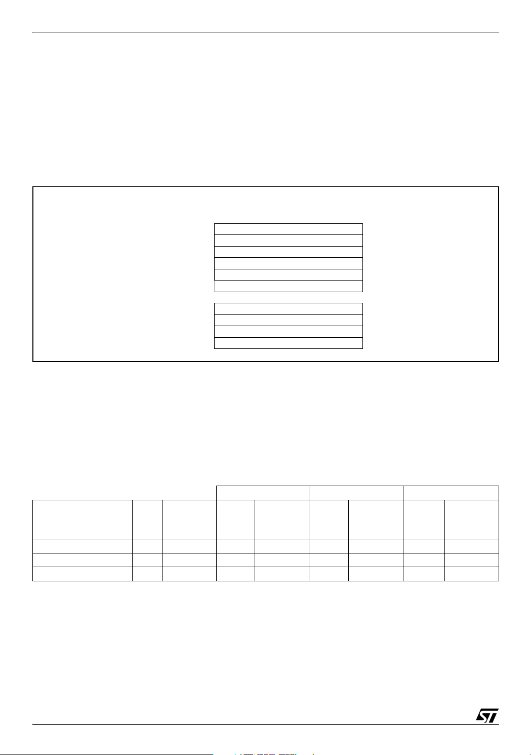
2.1 VECTOR TABLE
The first 16 words of the TestFlash contain the Vector Table.
The Power-On Vector is read when exiting from Reset. The Monitor Vector is read in Embedded Emulation Mode after an ETRAP instruction or an external Break. The NMI Vector is
read if a Non Maskable Interrupt occurs. The SCI Interrupt Vectors are used for the In-System
Programming routine.
Figure 2. Vector Table
Vector Table
230000h
230002h
230004h
230006h
230008h
23000Ah
230010h
230012h
230014h
230016h
Powe r-On Vector
Monitor Vector
NMI Vector
Mask Set Number
Device Identifier
TestFlash Code Revision
SCI Error Vector
SCI Address Match Vector
SCI Receiving End Vector
SCI Transmitting End Vector
2.1.1 Device identifier
This identifier contains the information about the device, its flash size and its reset vector location.
2.1.2 Testflash code revision
The CheckSum is the sum of all the bytes from 230000h to 230E77h, it can be used to verify
if the actual TestFlash content is the most recent one, or if the TestFlash content is corrupted.
rev 2.6 rev 2.7 rev 2.7.1
TF rev
(23000
Ah)
Testflash
checksum
Device
Flash
size
Device ID
(230008h)
ST92F124/F150 64K 1024h xx26h 933BFh xx27h 8FC55h 0127h 8FBEBh
ST92F124/F150 128K 1080h xx26h 9341Bh xx27h 8FCB1h 0127h 8FC47h
ST92F250 256K 1100h xx26h 9339Ch xx27h 8FC32h 0127h 8FBC8h
TF rev
(23000
Ah)
Testflash
checksum
TF rev
(23000
Ah)
Testflash
checksum
2.2 USER OTP AREA
The 124 bytes of TestFlash from 231F80h to 231FFBh are available to the User application as
One Time Programmable area (not erasable).
4/18
Page 5

ST92F120/F124/150/F250 TESTFLASH
2.3 PROTECTIONS
The TestFlash locations shown by the following figure have a special meaning related to the
Access and Write Flash Protection features (refer to the datasheets).
Figure 3. Protection Map
Protection
231FFCh
231FFDh
231FFEh NVPWD0
NVAPR
NVWPR
NVPWD1231FFFh
5/18
Page 6
ST92F120/F124/150/F250 TESTFLASH
3 ROUTINES DESCRIPTION
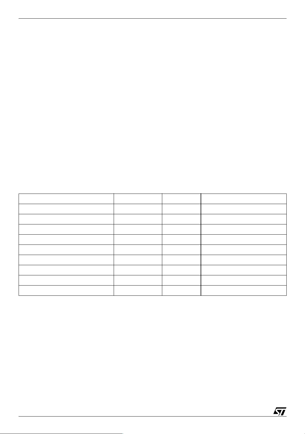
3.1 POWER-ON ROUTINE (230020H)
Inputs: None.
Outputs: R0, R1.
Variables: R2-R47, R160-R223 (for Stack).
Goal: to perform the initializations of ST9 device (Boot Code).
The Power-On routine is executed automatically when exiting reset.
The Power-On routine performs the following operations:
■ initialize the Stack Pointer in the Register File (for this reason, this routine modifies the
Registers of group A, B, C and D).
■ call the “E3
■ initialize the MMU paged registers as shown by the following table.
TM
Initialization routine“ (230026h).
Table 1. MMU Registers Initialization
Register Value Seg Notes
DPR0 - R240 00h 0h 1st 16k-page
DPR1 - R241 01h 0h 2nd 16k-page
DPR2 - R242 02h 0h 3rd 16k-page
DPR3 - R243 80h 20h 1st 16k-page
ISR - R248 00h 0h
DMASR - R249 20h 20h
MPSR - R250 21h 21h
MDPR0 - R251 84h 21h 1st 32k-page
MDPR1 - R252 86h 21h 2nd 32k-page
■ Set bit MEMSEL (bit 4) in the R246 (EMR2) register page 21
■ Set the Register Page Pointer to page 0.
■ Set Group 0 as working registers.
■ Set Program Memory.
■ read in 000000h the first word of segment 0h (Flash Memory), that is interpreted as the
Power-On Vector of the User application. (Warning: if the device identifier is equal to 0080h,
the User Reset Vector is read in 01E000h instead of in 000000h).
6/18
Page 7
ST92F120/F124/150/F250 TESTFLASH
■ check the value of the SOUT0 pin (SOUT pin of SCI0 macrocell): if it is low, the “Code
Update routine” is called.
■ check the Power-On Vector of the User application: if its value is FFFFh HALT instruction is
executed, otherwise the execution jumps into the location it points to.
The User Application should check the 2 Output variables of the Power-On routine:
The “E3
zation has been successful (Good Code: A4h), or if the E3
rupted (Bad Code: 40h) and the user software has to call the “E3
TM
Initialization routine” writes an output code in the R0 register to show if the initiali-
TM
NV Pointers are completely cor-
TM
Reset routine” (230032h).
The “Code Update routine” writes an output code in the R1 register to show if no update has
been requested or the update has been requested and the SCI communications have been
performed correctly (Good Code: 23h), or if the update has been requested, but the SCI communications has not been performed correctly in the timeout of 10ms (for a Fosc frequency of
4MHz) (Bad Code: 3Fh).
TM
Due to the “E3
Initialization routine”, the Power-On routine can last a long time. The typical
duration of the Power-On routine as a function of the external clock period Tck is shown in the
following table.
Table 2. Power-On routine typical duration
Condition
Normal operation (no E3 TM operation) 33 ms
SOUT0 pulled low, no code update 42 ms
Aborted E3 TM write operation (worst case) 165 ms (1)
(1) This duration depends also on E3 erasing
and programming times
Typical Power-on routine duration
with Fosc=4MHz
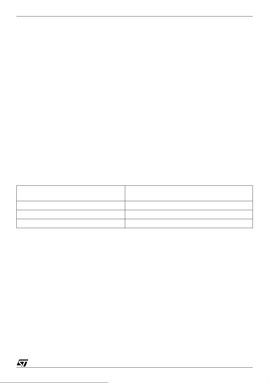
3.2 NON MASKABLE INTERRUPT ROUTINE
Inputs: None.
Outputs: None.
Variables: None.
Goal: react to a Non Maskable Interrupt when the Vector Table is remapped in TestFlash.
This routine should never be called, since the Vector Table is normally mapped in the Flash
address space.
This routine does not perform any operation, simply returns from interrupt.
7/18
Page 8

ST92F120/F124/150/F250 TESTFLASH
3.3 CODE UPDATE ROUTINE: IN-SYSTEM PROGRAMMING
Inputs: None.
Outputs: R1.
Variables: R4-R15, R208-R223 (for Stack).
Goal: in-system programming of the Flash memory content.
The Code Update routine is automatically called by the Power-On routine if the SOUT0 pad is
checked low.
The Code Update routine performs the following operations:
■ enable the SCI0 peripheral in synchronous mode;
■ transmit a synchronisation datum (25h);
■ wait for an address match (23h) with a timeout of 10ms (with an Fosc frequency of 4MHz).;
■ if the match is not received before the timeout, the execution returns to the Power-On routine
with an Error Code in the output register R1 (25h);
■ if the match is received, the SCI0 transmits a new datum (21h) to tell the external device that
it is ready to receive the data to be loaded in RAM (that represents the code of the in-system
programming routine);
■ receive two data bytes representing the number of bytes to be loaded (max 4Kbyte);
■ receive the specified number of bytes (each one preceded by the transmission of a Ready
to Receive character: 21h) and write them in internal RAM starting from address 200010h;
the first 4 words should be the interrupt vectors of the 4 possible SCI interrupts, to be used
by the in-system programming routine.
■ transmit a last datum (21h) as an end of communication request;
■ receive the end of communication confirmation datum (any byte other than 25h);
■ Reset all the unused Ram locations to FFh;
■ Call the address 200018h in internal RAM.
■ After completion of the in-system programming routine, an HALT instruction is executed and
a Hardware Reset is needed.
The Code Update routine initializes the SCI0 peripheral as shown in the following table:
Table 3. SCI0 Registers (page 24) initialization
8/18
Register Value Notes
IVR - R244 10h Vector Table in 0010h
ACR - R245 23h Address Match is 23h
IDPR - R249 00h SCI interrupt priority is 0
Page 9

Table 3. SCI0 Registers (page 24) initialization
Register Value Notes
CHCR - R250 83h 8 Data Bits
ST92F120/F124/150/F250 TESTFLASH
CCR - R251 E8h
BRGHR - R252 00h
BRGLR - R253 04h Baud Rate Divider is 4
SICR - R254 83h Synchronous Mode
SOCR - R255 01h
rec. clock: ext RXCLK0
trx clock: int CLKOUT0
The Code Update routine also remaps the interrupts in TestFlash (ISR = 23h), and configures
pins 3 (SOUT0) and 4 (CLKOUT0) of Port 5 as Alternate Function.
The Code Update routine uses 4 Interrupt routines: SCI Receiver Error Interrupt routine
(vector in 0010h), SCI Address Match Interrupt routine (vector in 0012h), SCI Receiver Data
Ready Interrupt routine (vector in 0014h), SCI Transmitter Buffer Empty Interrupt routine
(vector in 0016h).
TM
3.4 E3
INITIALIZATION ROUTINE (230026H)
Inputs: None.
Outputs: R0.
Variables: R1-R47, R160-R223 (for Stack).
TM
Goal: to initialize the E3
Hardware Emulation.
This routine is automatically called by the Power-On routine, but it can be also called by any
other routine through a far call:
CALLS 23h, 0026h ;E3TM Init
The E3TM Initialization routine performs the following operations:
■ read the NVCSS1 registers of sector E0 (229003h) and E1 (22D003h);
■ if the values of the two NVCSS1 registers are not coherent, the routine returns with the Error
TM
Code 40h, without completing the E3
■ if an aborted erase phase is detected, a Sector Erase operation is performed on the bad
Initialization;
sector;
■ write the VCSS1 register (222003h) with the sector number currently mapping the E3
TM
data;
■ read the NVCSS0 registers of sector E0 (229001h) and E1 (22D001h);
9/18
Page 10

ST92F120/F124/150/F250 TESTFLASH
■ if the values of the two NVCSS0 registers are not invalid, the routine returns with the Error
TM
Code 40h, without completing the E3
■ if an aborted erase phase is detected, a Sector Erase operation is performed on the bad
Initialization;
sector;
■ write the VCSS0 register (222001h) with the number of the last completed Erase Phase on
complementary sector;
■ read the NVESP0-63 registers of sector E0 (229000h-22907Eh) and E1 (22D000h-
22D07E);
■ if the values of a pair of NVESPX registers are invalid, the routine returns with the Error Code
40h, without completing the E3
■ if an aborted swap phase is detected, the swap is completed and a Sector Erase operation
TM
Initialization;
is performed on the old sector;
■ write each of the VESP0-63 registers (222000h-2223F0h) with the block number in which
the relative page is mapped;
■
each time an E3TM write operation is performed, a User routine is called to refresh an
external Watchdog if needed. 3.7 User routine for External Watchdog Refresh for details.
TM
The User Application should check the Output variable of the E3
Register R0 shows if the E3
TM
E3
NV Pointers are invalid and the initialization has not been completed (Bad Code: 40h).
In case of an initialization error, the E3
TM
a far call to the “E3
CALLS 23h, 0032h ;E3TM Reset
Reset routine” (230032h):
TM
initialization has been possible (Good Code: A4h), or if the
TM
NV pointers can be reset to a valid content through
Initialization routine:
Note that in this case, any data present in the E3TM is lost.
10/18
Page 11
ST92F120/F124/150/F250 TESTFLASH
3.5 E3TM SWAP ERROR ROUTINES
3.5.1 Find Wrong Pages (230029h)
Inputs: None.
Outputs: R16-R23.
Variables: R192-R223 (for Stack).
Goal: to find the pages in which some new data are different from the old ones after a Swap
fail.
This routine has to be called by the User application if bits FEERR of FESR0 (224002h) reg-
TM
ister and SWER of FESR1 (224003h) register are set after an E3
write operation. It can be
called through a far call:
CALLS 23h, 0029h ;Find Wrong Pages
This routine performs the following operations:
■ initialize a Page counter (from 00h to 3Fh);
■ read the 16 bytes of the current Page in the new block (new data after Swap);
■ read the 16 bytes of the current Page in the old block (old data before Swap);
■ if at least one of the new and old data differs, set the output flag corresponding to the current
Page;
■ increment the Page counter and repeat the 3 preceding steps, untill the last Page is
reached;
The User Application should check the 8 Output variables, which are explained in the following
table:
Table 4. Wrong Pages Output Meaning
Reg Bit 0 Meaning 1 Meaning
R16 0 Page 00h OK Page 00h Wrong
R16 X Pg 00h+X OK Pg 00h+X Wrong
R16 7 Page 07h OK Page 07h Wrong
R17 0 Page 08h OK Page 08h Wrong
R17 X Pg 08h+X OK Pg 08h+X Wrong
R17 7 Page 0Fh OK Page 0Fh Wrong
R18 X Pg 10h+X OK Pg 10h+X Wrong
R19 X Pg 18h+X OK Pg 18h+X Wrong
R20 X Pg 20h+X OK Pg 20h+X Wrong
R21 X Pg 28h+X OK Pg 28h+X Wrong
11/18
Page 12

ST92F120/F124/150/F250 TESTFLASH
Table 4. Wrong Pages Output Meaning
Reg Bit 0 Meaning 1 Meaning
R22 0 Page 30h OK Page 30h Wrong
R22 X Pg 30h+X OK Pg 30h+X Wrong
R22 7 Page 37h OK Page 37h Wrong
R23 0 Page 38h OK Page 38h Wrong
R23 X Pg 38h+X OK Pg 38h+X Wrong
R23 7 Page 3Fh OK Page 3Fh Wrong
3.5.2 Find Wrong Bytes (23002Ch)
Inputs: R2-R3.
Outputs: R0-R1.
Variables: R192-R223 (for Stack).
Goal: to find in the specified page the bytes different from the old ones after a Swap fail.
This routine has to be called by the User application if bits FEERR of FESR0 (224002h) reg-
TM
ister and SWER of FESR1 (224003h) register are set after an E3
write operation. After
having executed the “Find Wrong Pages routine”, this routine can be called through a far call,
providing as input in RR2 the address of the first byte of the Page to check:
LDW RR2, #01C0h;If Page 1Ch is wrong
CALLS 23h, 002Ch ;Find Wrong Bytes
This routine performs the following operations:
■ initialize a Byte counter (from 0h to Fh);
■ read the current Byte in the new block (new data after Swap);
■ read the current Byte in the old block (old data before Swap);
■ if the new and old data differs, set the output flag corresponding to the current Byte;
■ increment the Byte counter and repeat the 3 preceding steps, untill the last Byte is reached;
The User Application should check the 2 Output variables, which are explained in the following
table:
Table 5. Wrong Bytes Output Meaning
Reg Bit 0 Meaning 1 Meaning
R1 0 Byte 0h OK Byte 0h Wrong
R1 X Byte 0h+X OK Byte 0h+X Wrong
R1 7 Byte 7h OK Byte 7h Wrong
R0 0 Byte 8h OK Byte 8h Wrong
12/18
Page 13

ST92F120/F124/150/F250 TESTFLASH
Table 5. Wrong Bytes Output Meaning
Reg Bit 0 Meaning 1 Meaning
R0 X Byte 8h+X OK Byte 8h+X Wrong
R0 7 Byte Fh OK Byte Fh Wrong
3.5.3 Complete Aborted Swap (23002Fh)
Inputs: None.
Outputs: R0.
Variables: R192-R223 (for Stack).
Goal: complete the aborted Swap Phase after a Swap fail.
TM
This routine has to be called by the User application if after an E3
write operation the bits
FEERR of FESR0 (224002h) and SWER of FESR1 (224003h) are set. After having executed
the “Find Wrong Pages routine” and the “Find Wrong Bytes routine”, and after having stored in
TM
Ram the E3
addresses and data to program again, this routine can be called through a far
call:
CALLS 23h, 002Fh ;Complete Swap
This routine performs the following operations:
■ perform a Sector Erase operation on the old sector;
■ during the Sector Erase operation, a User routine is called toy refresh an external Watchdog
if necessary. 3.7 User routine for External Watchdog Refresh for details.
■ write the VCSS1 register (222003h) with the sector number currently mapping the E3
TM
data;
■ write the VCSS0 register (222001h) with the number of the last completed Erase Phase on
the complementary sector;
The User Application should check the Output variable of the Complete Swap routine:
Register R0 shows if the Sector Erase operation has been completed correctly (Good Code:
A4h), or if has failed (Bad Code: 40h).
13/18
Page 14

ST92F120/F124/150/F250 TESTFLASH
3.6 E3TM RESET TO DELIVERY STATUS (230032H)
Inputs: None.
Outputs: R0.
Variables: R192-R223 (for Stack).
Goal: erase sectors E0 and E1 and program the NV pointers so that E0 is the current sector
with all the Pages mapped in block 0 and E1 is completely erased.
TM
This routine has to be called by the User application if the E3
NV Pointers have lost any coherence and can be no more correctly interpreted by the “Power-On routine”. This routine can
be called through a far call:
CALLS 23h, 0032h ;E3TM Reset
This routine performs the following operations:
■ perform a Sector Erase operation on sector E0;
■ perform a Sector Erase operation on sector E1;
■ program FDh in the NVCSS1 register of sector E0 (229003h);
■ write 00h in the VCSS1 register (222003h): E0 is the sector currently mapping the E3
TM
data;
■ program 00h in the NVCSS0 register of sector E0 (229001h);
■ write 30h in the VCSS0 register (222001h): Erase Phase 3 has been completed on
complementary sector E1;
■ program EEh in the NVESP0-63 registers of sector E0 (229000h-22907Eh);
■ write 00h in the VESP0-63 registers (222000h-2223F0h): all Pages are mapped in block 0
of sector E0;
■ each time an E3
TM
write operation is performed, a User routine is called to eventually refresh
an external Watchdog. 3.7 User routine for External Watchdog Refresh for details.
TM
The User Application should check the Output variable of the E3
Reset routine:
Register R0 shows if the Sector Erase operations have been completed correctly (Good
Code: A4h), or if have failed (Bad Code: 40h).
14/18
Page 15
ST92F120/F124/150/F250 TESTFLASH
3.7 USER ROUTINE FOR EXTERNAL WATCHDOG REFRESH
Inputs: None.
Outputs: None.
Variables: None.
Goal: to refresh the external Watchdog during the BootRom code execution.
This routine has to be written by the User in Flash. The address where the routine starts has
to be written in 000006h (1 word), while the segment where the routine is located has to be
written in 000009h (1 byte).
This routine is called at least once every time that the BootRom execution performs an E3
TM
write operation. If the write operations has a long duration, the User routine is called with a rate
fixed by location 000008h: with an internal clock frequency of 2MHz, location 000008h fixes
the number of milliseconds to wait between two calls of the User routine.
Table 6. User routine parameters
Location Size Notes
000006h 2 byte User routine address
000008h 1 byte ms rate at 2MHz
000009h 1 byte User routine segment
If location 000006h is virgin (FFFFh), the User routine is not called.
TM
The user routine is called only by the E3
TM
Reset routine) in testflash revisions 2.5 and 2.6, but is also called by the E3TM initializa-
E3
management routines (E3TM Swap Error Routines,
tion routine at Power on in testflash version 2.5.
To avoid modifying the User initialization, when the BootRom code calls the User routine, it
does not perform the standard initializations:
■ The MMU paged registers are set as shown by the following table.
Table 7. MMU Registers Initialization
Register Value Seg Notes
DPR0 - R240 00h 0h 1st 16k-page
DPR1 - R241 89h 22h 2nd 16k-page
DPR2 - R242 8Ah 22h 3rd 16k-page
DPR3 - R243 8Bh 22h 4th 16k-page
ISR - R248 XXh XXh not modified
DMASR - R249 XXh XXh not modified
15/18
Page 16
ST92F120/F124/150/F250 TESTFLASH
Table 7. MMU Registers Initialization
Register Value Seg Notes
MPSR - R250 XXh XXh not modified
MDPR0 - R251 XXh XXh not modified
MDPR1 - R252 XXh XXh not modified
■ Bit MEMSEL (bit 4) of R246 (EMR2) page 21 is not modified.
■ The Register Page Pointer is set to page 21.
■ Group 0 is set as the working register group.
■ Data Memory is Set.
The User routine must avoid modifying the context of the BootRom routine. The following registers must not be modified when the User routine returns:
■ System Stack Pointer: RR238.
■ Page Pointer: R234.
■
Register Pointers: RR232.
■ Bit 0 of Flag Register: R231.
■ Data Page Pointers DPR0-3.
■ Registers of Groups 0 and 1.
16/18
Page 17

ST92F120/F124/150/F250 TESTFLASH
4 E3TM FAILURE RECOVERY
4.1 ERASE OR WRITE ERROR: FATAL ERROR
TM
ST guarantees 100 000 erase cycles endurance for the E3
write cycles for the most updated page (1 page contains 16 bytes). But after this period, an
erase error or a write error may occur. This error is due to one or several flash cells that cannot
be erased (logic level 1) or programmed (logic level 0) anymore. This is a hardware failure and
the only workaround is to not use these bytes, which means that the data must be relocated.
As each time a data is updated, the whole page is recopied, consequently the whole page
should be remapped in order to avoid any erase/write error at the same location.
4.2 SWAP ERROR: NON FATAL ERROR
TM
A swap error may occur during the E3
fied in any application using the Emulated E3
product life. Till now, no swap error has been identi-
TM
of the ST9. Anyway, this error is not fatal and
there are 2 ways to recover:
, which correponds to 800 000
4.2.1 Generate a reset
Generating a software reset will automatically execute the testflash, which will complete the
TM
E3
swap operation. It will restore the E3TM content as it was before the last writing attempt,
which means that the last updated data is lost.
4.2.2 Call the “complete aborted swap phase” routine in testflash.
The fastest way to complete the swap operation is to call the routine “complete aborted swap
phase” directly in testflash. This is done by the instruction:
CALLS 0x23, 0x002F ;Complete Swap
The “complete aborted swap phase” routine will restore the E3TM content as it was before the
last write attempt, which means that the last updated data is lost. It is possible for the user to
find exactly what was the last page and byte written by calling the routines “Find wrong page”
and then “Find wrong byte”.
17/18
Page 18

ST92F120/F124/150/F250 TESTFLASH
“THE PRESENT NOTE WHICH IS FOR GUIDANCE ONLY AIMS AT PROVIDING CUSTOMERS WITH INFORMATION
REGARDING THEIR PRODUCTS IN ORDER FOR THEM TO SAVE TIME. AS A RESULT, STMICROELECTRONICS
SHALL NOT BE HELD LIABLE FOR ANY DIRECT, INDIRECT OR CONSEQUENTIAL DAMAGES WITH RESPECT TO
ANY CLAIMS ARISING FROM THE CONTENT OF SUCH A NOTE AND/OR THE USE MADE BY CUSTOMERS OF
THE INFORMATION CONTAINED HEREIN IN CONNECTION WITH THEIR PRODUCTS.”
Information furnished is believed to be accurate and reliable. However, STMicroelectronics assumes no responsibility for the consequences
of use of such information nor for any infringement of patents or other rights of third parties which may result from its use. No license is granted
by implication or otherwise under any patent or patent rights of STMicroelectronics. Specifications mentioned in this publication are subject
to change without notice. This publication supersedes and replaces all information previously supplied. STMicroelectronics products are not
authorized for use as critical components in life support devices or systems without express written approval of STMicroelectronics.
The ST logo is a registered trademark of STMicroelectronics.
All other names are the property of their respective owners
© 2005 STMicroelectronics - All rights reserved
STMicroelectronics group of companies
Australia – Belgium - Brazil - Canada - China – Czech Republic - Finland - France - Germany - Hong Kong - India - Israel - Italy - Japan -
Malaysia - Malta - Morocco - Singapore - Spain - Sweden - Switzerland - United Kingdom - United States of America
www.st.com
18/18
 Loading...