

Page 1
AN1517
Application note
Designing with the L5972D high efficiency DC-DC converter
Introduction
The L5972D is a step-down monolithic power switching regulator capable of delivering up to
2 A at output voltages from 1.235 V to 35 V. The operating input voltage ranges from 4.4 V to
36 V. It has been designed using BCDV technology and the power switching element is
implemented through a P-channel DMOS transistor. It does not require a bootstrap
capacitor, and the duty cycle can range up to 100%. An internal oscillator fixes the switching
frequency at 250 kHz. This minimizes the LC output filter.
Pulse-by-pulse and frequency foldback over-current protection offer effective protection
against short-circuit. Other features are voltage feed-forward, protection against feedback
disconnection, and thermal shutdown. The device is housed in a thermally improved SO-8
package (with 4 pins connected to GND so that the thermal resistance junction-to-ambient
is reduced to approximately one-half compared with a standard SO-8 package.
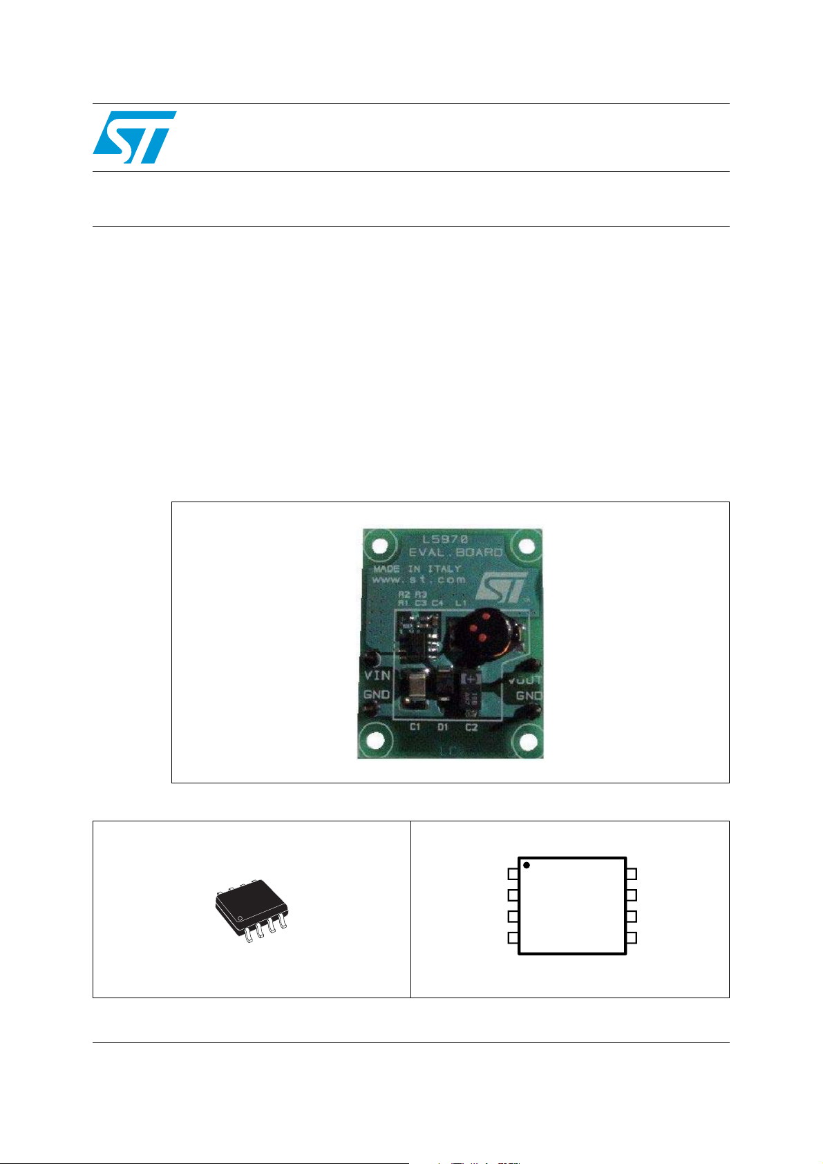
Figure 1. Demonstration board
L5972D (SO-8) Board dimensions: 23 x 20 mm
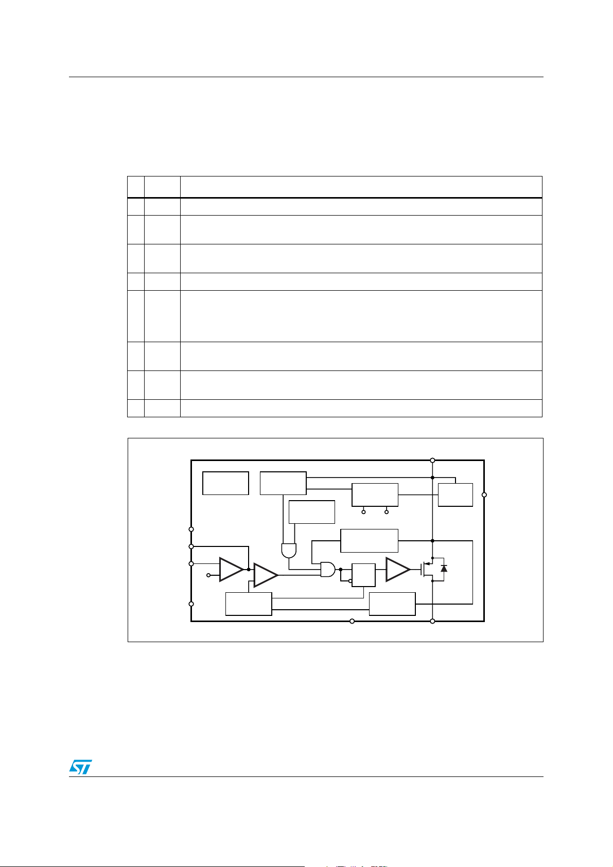
Figure 2. Package Figure 3. Pin connection
May 2008 Rev 2 1/29
VCC
8
7
6
5
AM00004v1
GND
VREF
FB
www.st.com
SO-8
OUT
SYNC
INH
COMP
1
2
3
4
Page 2

Contents AN1517
Contents
1 Pin functions . . . . . . . . . . . . . . . . . . . . . . . . . . . . . . . . . . . . . . . . . . . . . . . 5
1.1 Pin description . . . . . . . . . . . . . . . . . . . . . . . . . . . . . . . . . . . . . . . . . . . . . . 5
2 Functional description . . . . . . . . . . . . . . . . . . . . . . . . . . . . . . . . . . . . . . . 6
2.1 Power supply and voltage reference . . . . . . . . . . . . . . . . . . . . . . . . . . . . . 6
2.2 Voltages monitor . . . . . . . . . . . . . . . . . . . . . . . . . . . . . . . . . . . . . . . . . . . . . 6
2.3 Oscillator . . . . . . . . . . . . . . . . . . . . . . . . . . . . . . . . . . . . . . . . . . . . . . . . . . 7
2.4 Current protection . . . . . . . . . . . . . . . . . . . . . . . . . . . . . . . . . . . . . . . . . . . . 7
2.5 Error amplifier . . . . . . . . . . . . . . . . . . . . . . . . . . . . . . . . . . . . . . . . . . . . . . . 8
2.6 PWM comparator and power stage . . . . . . . . . . . . . . . . . . . . . . . . . . . . . . 8
2.7 Thermal shutdown . . . . . . . . . . . . . . . . . . . . . . . . . . . . . . . . . . . . . . . . . . . 9
3 Additional features and protection . . . . . . . . . . . . . . . . . . . . . . . . . . . . 10
3.1 Feedback disconnection . . . . . . . . . . . . . . . . . . . . . . . . . . . . . . . . . . . . . . 10
3.2 Output over-voltage protection . . . . . . . . . . . . . . . . . . . . . . . . . . . . . . . . . 10
3.3 Zero load . . . . . . . . . . . . . . . . . . . . . . . . . . . . . . . . . . . . . . . . . . . . . . . . . 10
4 Closing the loop . . . . . . . . . . . . . . . . . . . . . . . . . . . . . . . . . . . . . . . . . . . 11
4.1 Error amplifier and compensation network . . . . . . . . . . . . . . . . . . . . . . . . 11
4.2 LC filter . . . . . . . . . . . . . . . . . . . . . . . . . . . . . . . . . . . . . . . . . . . . . . . . . . . 12
4.3 PWM comparator . . . . . . . . . . . . . . . . . . . . . . . . . . . . . . . . . . . . . . . . . . . 13
5 Application information . . . . . . . . . . . . . . . . . . . . . . . . . . . . . . . . . . . . . 16
5.1 Component selection . . . . . . . . . . . . . . . . . . . . . . . . . . . . . . . . . . . . . . . . 16
5.1.1 Input capacitor . . . . . . . . . . . . . . . . . . . . . . . . . . . . . . . . . . . . . . . . . . . . 16
5.1.2 Output capacitor . . . . . . . . . . . . . . . . . . . . . . . . . . . . . . . . . . . . . . . . . . 17
5.1.3 Inductor . . . . . . . . . . . . . . . . . . . . . . . . . . . . . . . . . . . . . . . . . . . . . . . . . 17
5.2 Layout considerations . . . . . . . . . . . . . . . . . . . . . . . . . . . . . . . . . . . . . . . . 18
5.3 Thermal considerations . . . . . . . . . . . . . . . . . . . . . . . . . . . . . . . . . . . . . . 19
5.4 Short-circuit protection . . . . . . . . . . . . . . . . . . . . . . . . . . . . . . . . . . . . . . . 20
5.5 Application circuit . . . . . . . . . . . . . . . . . . . . . . . . . . . . . . . . . . . . . . . . . . . 21
6 Application ideas . . . . . . . . . . . . . . . . . . . . . . . . . . . . . . . . . . . . . . . . . . . 24
2/29
Page 3

AN1517 Contents
6.1 Positive buck-boost regulator . . . . . . . . . . . . . . . . . . . . . . . . . . . . . . . . . . 24
7 Buck-boost regulator . . . . . . . . . . . . . . . . . . . . . . . . . . . . . . . . . . . . . . . 24
7.1 Dual output voltage with auxiliary winding . . . . . . . . . . . . . . . . . . . . . . . . 25
8 Compensation network with MLCC (multiple layer ceramic capacitor) at
the output . . . . . . . . . . . . . . . . . . . . . . . . . . . . . . . . . . . . . . . . . . . . . . . . . 26
8.1 External soft-start network . . . . . . . . . . . . . . . . . . . . . . . . . . . . . . . . . . . . 26
9 Revision history . . . . . . . . . . . . . . . . . . . . . . . . . . . . . . . . . . . . . . . . . . . 28
3/29
Page 4

List of figures AN1517
List of figures
Figure 1. Demonstration board . . . . . . . . . . . . . . . . . . . . . . . . . . . . . . . . . . . . . . . . . . . . . . . . . . . . . . 1
Figure 2. Package . . . . . . . . . . . . . . . . . . . . . . . . . . . . . . . . . . . . . . . . . . . . . . . . . . . . . . . . . . . . . . . . 1
Figure 3. Pin connection . . . . . . . . . . . . . . . . . . . . . . . . . . . . . . . . . . . . . . . . . . . . . . . . . . . . . . . . . . . 1
Figure 4. Block diagram . . . . . . . . . . . . . . . . . . . . . . . . . . . . . . . . . . . . . . . . . . . . . . . . . . . . . . . . . . . . 5
Figure 5. Internal regulator circuit . . . . . . . . . . . . . . . . . . . . . . . . . . . . . . . . . . . . . . . . . . . . . . . . . . . . 7
Figure 6. Oscillator circuit block diagram . . . . . . . . . . . . . . . . . . . . . . . . . . . . . . . . . . . . . . . . . . . . . . . 7
Figure 7. Current limitation circuitry . . . . . . . . . . . . . . . . . . . . . . . . . . . . . . . . . . . . . . . . . . . . . . . . . . . 8
Figure 8. Driving circuitry . . . . . . . . . . . . . . . . . . . . . . . . . . . . . . . . . . . . . . . . . . . . . . . . . . . . . . . . . . . 9
Figure 9. Block diagram of the loop . . . . . . . . . . . . . . . . . . . . . . . . . . . . . . . . . . . . . . . . . . . . . . . . . . 11
Figure 10. Error amplifier equivalent circuit and compensation network . . . . . . . . . . . . . . . . . . . . . . . 12
Figure 11. Module plot . . . . . . . . . . . . . . . . . . . . . . . . . . . . . . . . . . . . . . . . . . . . . . . . . . . . . . . . . . . . . 14
Figure 12. Phase plot . . . . . . . . . . . . . . . . . . . . . . . . . . . . . . . . . . . . . . . . . . . . . . . . . . . . . . . . . . . . . . 15
Figure 13. Layout example . . . . . . . . . . . . . . . . . . . . . . . . . . . . . . . . . . . . . . . . . . . . . . . . . . . . . . . . . 18
Figure 14. Short-circuit current V
Figure 15. Short-circuit current V
Figure 16. Demonstration board application circuit . . . . . . . . . . . . . . . . . . . . . . . . . . . . . . . . . . . . . . . 21
Figure 17. PCB layout (component side) . . . . . . . . . . . . . . . . . . . . . . . . . . . . . . . . . . . . . . . . . . . . . . . 22
Figure 18. PCB layout (bottom side) . . . . . . . . . . . . . . . . . . . . . . . . . . . . . . . . . . . . . . . . . . . . . . . . . . 22
Figure 19. PCB layout (front side) . . . . . . . . . . . . . . . . . . . . . . . . . . . . . . . . . . . . . . . . . . . . . . . . . . . . 23
Figure 20. Junction temperature vs. output current . . . . . . . . . . . . . . . . . . . . . . . . . . . . . . . . . . . . . . . 23
Figure 21. Junction temperature vs. output current . . . . . . . . . . . . . . . . . . . . . . . . . . . . . . . . . . . . . . . 23
Figure 22. Junction temperature vs. output current . . . . . . . . . . . . . . . . . . . . . . . . . . . . . . . . . . . . . . . 23
Figure 23. Efficiency vs. output current . . . . . . . . . . . . . . . . . . . . . . . . . . . . . . . . . . . . . . . . . . . . . . . . 23
Figure 24. Positive buck-boost regulator . . . . . . . . . . . . . . . . . . . . . . . . . . . . . . . . . . . . . . . . . . . . . . . 24
Figure 25. Buck-boost regulator. . . . . . . . . . . . . . . . . . . . . . . . . . . . . . . . . . . . . . . . . . . . . . . . . . . . . . 24
Figure 26. Dual output voltage with auxiliary winding . . . . . . . . . . . . . . . . . . . . . . . . . . . . . . . . . . . . . 25
Figure 27. MLCC compensation network example . . . . . . . . . . . . . . . . . . . . . . . . . . . . . . . . . . . . . . . 26
Figure 28. Soft-start network example . . . . . . . . . . . . . . . . . . . . . . . . . . . . . . . . . . . . . . . . . . . . . . . . . 27
= 25 V. . . . . . . . . . . . . . . . . . . . . . . . . . . . . . . . . . . . . . . . . . . . . . 21
IN
= 30 V. . . . . . . . . . . . . . . . . . . . . . . . . . . . . . . . . . . . . . . . . . . . . . 21
IN
4/29
Page 5
AN1517 Pin functions
1 Pin functions
1.1 Pin description
Table 1. Pin description
N. Name Description
1 OUT Regulator output.
2GND
Ground. Lead connected directly to the frame in order to reduce the junction-to-ambient
thermal resistance.
3GND
Ground. Lead connected directly to the frame in order to reduce the junction-to-ambient
thermal resistance.
4 COMP E/A output to be used for frequency compensation.
Step-down feedback input. Connecting the output voltage directly to this pin results in
5FB
an output voltage of 1.235 V. An external resistor divider is required for higher output
voltages (the typical value for the resistor connected between this pin and ground is
4.7 k).
6GND
7GND
8V
Ground. Lead connected directly to the frame in order to reduce the junction-to-ambient
thermal resistance.
Ground. Lead connected directly to the frame in order to reduce the junction-to-ambient
thermal resistance.
Unregulated DC input voltage.
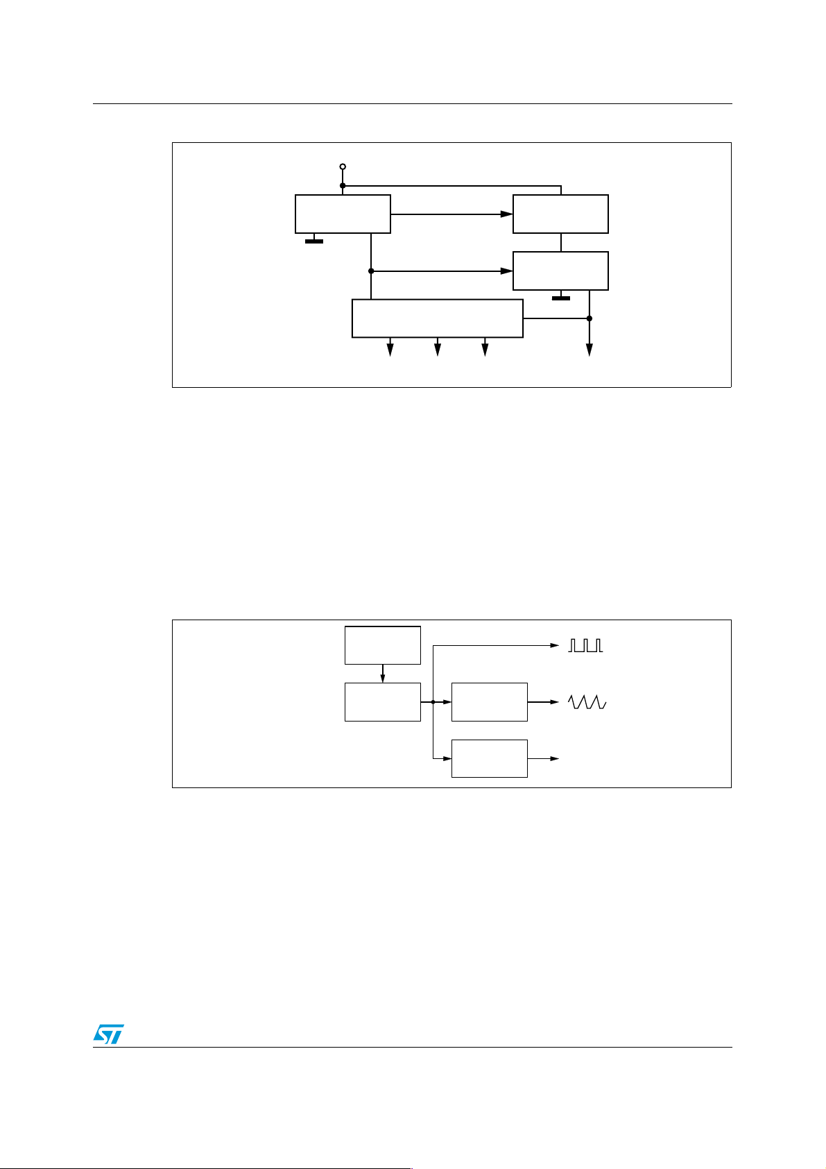
CC
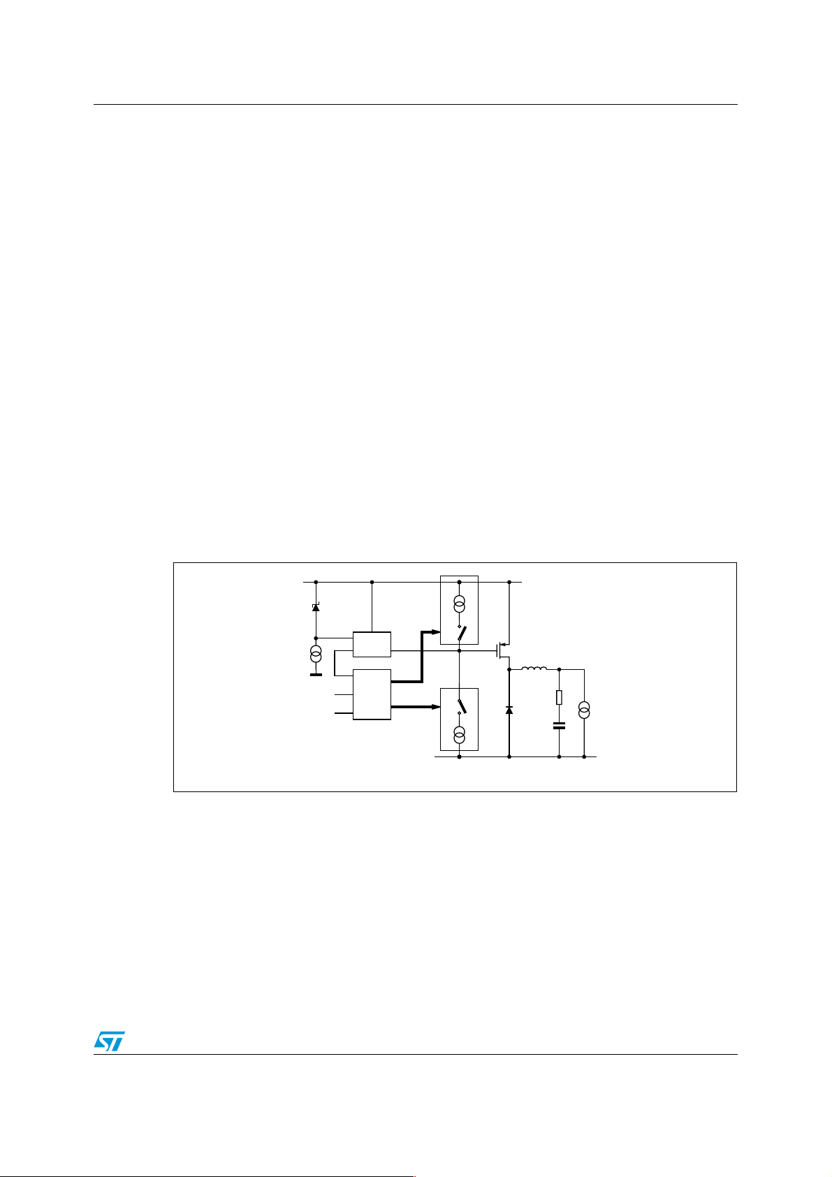
Figure 4. Block diagram
VOLTAGES
MONITOR
PWM
+
-
THERMAL
SHUTDOWN
SUPPLY
1.235V 3.5V
PEAK TO PEAK
CURRENT LIMIT
DCkQ
GND
COMP
FB
GND
TRIMMING
1.235V
E/A
-
+
OSCILLATOR
DRIVER
FREQUENCY
SHIFTER
VCC
V
REF
BUFFER
LPDMOS
POWER
GND
GND OUT
AM00028v1
5/29
Page 6

Functional description AN1517
2 Functional description
The main internal blocks are shown in the device block diagram in Figure 4. They are:
● A voltage regulator that supplies the internal circuitry. From this regulator, a 3.3 V
reference voltage is externally available.
● A voltage monitor circuit which checks the input and internal voltages.
● A fully integrated sawtooth oscillator with a frequency of 250 kHz ±15%, including also
the voltage feed-forward function and an input/output synchronization pin.
● Two embedded current limitation circuits which control the current that flows through
the power switch. The pulse-by-pulse current limit forces the power switch OFF cycle
by cycle if the current reaches an internal threshold, while the frequency shifter reduces
the switching frequency in order to significantly reduce the duty cycle.
● A transconductance error amplifier.
● A pulse width modulation (PWM) comparator and the relative logic circuitry necessary
to drive the internal power.
● A high-side driver for the internal P-MOS switch.
● A circuit to implement the thermal protection function.
2.1 Power supply and voltage reference
The internal regulator circuit (shown in Figure 5) consists of a start-up circuit, an internal
voltage Preregulator, the Bandgap voltage reference and the Bias block that provides
current to all the blocks.
The Starter gives the start-up currents to the entire device when the input voltage goes high
and the device is enabled (inhibit pin connected to ground).
The Preregulator block supplies the Bandgap cell with a preregulated voltage V
a very low supply voltage noise sensitivity.
2.2 Voltages monitor
An internal block continuously senses the VCC, V
their thresholds, the regulator begins operating. There is also a hysteresis on the V
(UVLO).
and VBG. If the voltages go higher than
REF
REG
that has
CC
6/29
Page 7
AN1517 Functional description
Figure 5. Internal regulator circuit
V
CC
2.3 Oscillator
Figure 6 shows the block diagram of the oscillator circuit.
The Clock Generator provides the switching frequency of the device, which is internally fixed
at 250 kHz. The Frequency Shifter block acts to reduce the switching frequency in case of
strong over-current or short-circuit. The clock signal is then used in the internal logic
circuitry and is the input of the Ramp Generator.
The Ramp Generator circuit provides the sawtooth signal, used to for PWM control and the
internal voltage feed-forward.
Figure 6. Oscillator circuit block diagram
STARTER
PREREGULATOR
VREG
BANDGAP
IC BIAS
VREF
AM00006v1
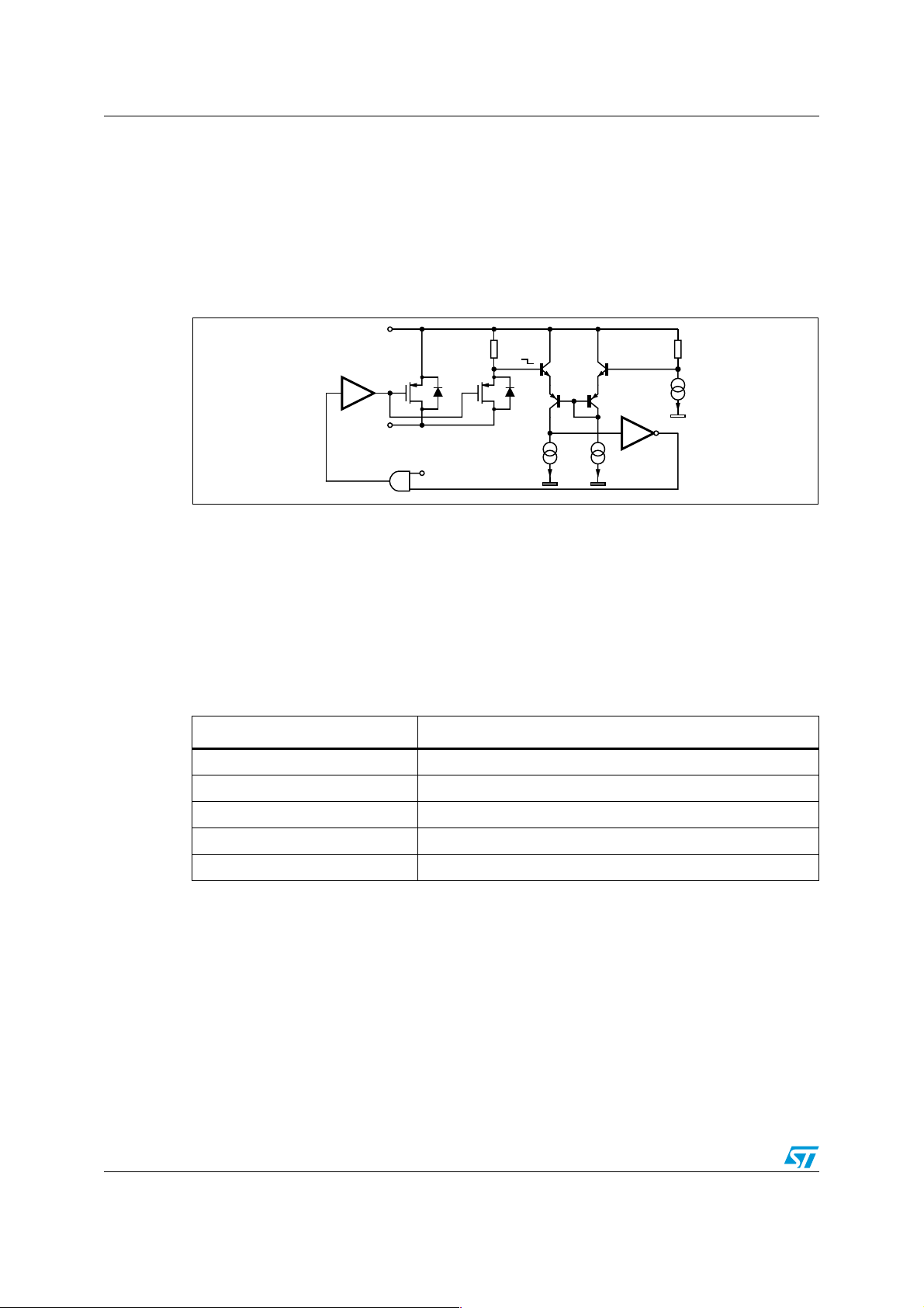
2.4 Current protection
The L5973AD has two types of current limit protection: pulse-by-pulse and frequency
foldback.
The schematic of the current limitation circuitry for the pulse-by-pulse protection is shown in
Figure 7. The output power PDMOS transistor is split into two parallel PDMOS transistors.
The smallest one includes a resistor in series, R
R
switched off until the next falling edge of the internal clock pulse.
and if it reaches the threshold, the mirror becomes unbalanced and the PDMOS is
SENSE
FREQUENCY
Ibias_osc
GENERATOR
FREQUENCY
SHIFTER
SHIFTER
CLOCK
CLOCK
GENERATOR
RAMP
RAMP
GENERATOR
GENERATOR
SYNCHRONIZATOR
SYNCHRONIZER
. The current is sensed through
SENSE
CLOCK
RAMP
SYNC
t
AM00007v1
7/29
Page 8
Functional description AN1517
Due to this reduction of the ON time, the output voltage decreases.
Since the minimum switch ON time (necessary to avoid a false over-current signal) is too
short to obtain a sufficiently low duty cycle at 250 kHz, the output current, in strong overcurrent or short-circuit conditions, could increase again. For this reason the switching
frequency is also reduced, thus keeping the inductor current under its maximum threshold.
The Frequency Shifter (Figure 6) functions based on the feedback voltage. As the feedback
voltage decreases (due to the reduced duty cycle), the switching frequency decreases also.
Figure 7. Current limitation circuitry
VCC
DRIVER
OUT
A1/A2=95
PWM
RSENSE
A1
A2
I
OFF
II
RTH
I
NOT
AM00008v1
L
2.5 Error amplifier
The voltage error amplifier is the core of the loop regulation. It is a transconductance
operational amplifier whose non inverting input is connected to the internal voltage
reference (1.235 V), while the inverting input (FB) is connected to the external divider or
directly to the output voltage. The output (COMP) is connected to the external compensation
network. The uncompensated error amplifier has the following characteristics:
Table 2. Uncompensated error amplifier characteristics
Description Values
Transconductance 2300 µS
Low frequency gain 65 dB
Minimum sink/source voltage 1500 µA/300 µA
Output voltage swing 0.4 V/3.65 V
Input bias current 2.5 µA
The error amplifier output is compared with the oscillator sawtooth to perform PWM control.
2.6 PWM comparator and power stage
This block compares the oscillator sawtooth and the error amplifier output signals
generating the PWM signal for the driving stage.
The power stage is a highly critical block, as it functions to guarantee a correct turn ON and
turn OFF of the PDMOS. The turn ON of the power element, or more accurately, the rise
time of the current at turn ON, is a very critical parameter. At a first approach, it appears that
8/29
Page 9
AN1517 Functional description
the faster the rise time, the lower the turn ON losses. However, there is a limit introduced by
the recovery time of the recirculation diode.
In fact, when the current of the power element is equal to the inductor current, the diode
turns OFF and the drain of the power is able to go high. But during its recovery time, the
diode can be considered a high value capacitor and this produces a very high peak current,
responsible for many problems:
● Spikes on the device supply voltage that cause oscillations (and thus noise) due to the
board parasitics
● Turn ON over-current leads to a decrease in the efficiency and system reliability
● Major EMI problems
● Shorter freewheeling diode life
The fall time of the current during the turn OFF is also critical, as it produces voltage spikes
(due to the parasitics elements of the board) that increase the voltage drop across the
PDMOS.
In order to minimize these problems, a new driving circuit topology has been used and the
block diagram is shown in Figure 8. The basic idea is to change the current levels used to
turn the power switch ON and OFF, based on the PDMOS and the gate clamp status.
This circuitry allows the power switch to be turned OFF and ON quickly and addresses the
freewheeling diode recovery time problem. The gate clamp is necessary to avoid that V
the internal switch goes higher than V
max. The ON/OFF Control block protects against
GS
GS
of
any cross conduction between the supply line and ground.
Figure 8. Driving circuitry
Vgs
STOP
DRIVE
DRAIN
2.7 Thermal shutdown
The Thermal Shutdown block generates a signal that turns OFF the power stage if the
temperature of the chip goes higher than a fixed internal threshold (150 °C). The sensing
element of the chip is very close to the PDMOS area, ensuring fast and accurate
temperature detection. A hysteresis of approximately 20 °C avoids that the device turns ON
and OFF continuously.
max
CLAMP
ON/OFF
CONTROL
GATE
OFF
ON
I
OFF
DRAIN
I
ON
VCC
PDMOS
ESR
C
VOUT
AM00009v1
I
LOAD
L
9/29
Page 10

Additional features and protection AN1517
3 Additional features and protection
3.1 Feedback disconnection
If the feedback is disconnected, the duty cycle increases towards the maximum allowed
value, bringing the output voltage close to the input supply. This condition could destroy the
load.
To avoid this hazardous condition, the device is turned OFF if the feedback pin is left
floating.
3.2 Output over-voltage protection
Over-voltage protection, or OVP, is achieved by using an internal comparator connected to
the feedback, which turns OFF the power stage when the OVP threshold is reached. This
threshold is typically 30% higher than the feedback voltage.
When a voltage divider is required to adjusting the output voltage (Figure 14), the OVP
intervention will be set at:
Equation 1
R1R2+
V
OVP
1.3
--------------------- -
• VFB•=
R
2
Where R
R
is between the feedback pin and ground.
2
is the resistor connected between the output voltage and the feedback pin, while
1
3.3 Zero load
Due to the fact that the internal power is a PDMOS, no bootstrap capacitor is required and
so the device works properly even with no load at the output. In this condition it works in
burst mode, with random burst repetition rate.
10/29
Page 11

AN1517 Closing the loop
4 Closing the loop
Figure 9. Block diagram of the loop
4.1 Error amplifier and compensation network
The output L-C filter of a step-down converter contributes with 180 degrees phase shift in
the control loop. For this reason a compensation network between the COMP pin and
GROUND is added. The simplest compensation network together with the equivalent circuit
of the error amplifier are shown in Figure 10. R
open loop gain. CP does not significantly affect system stability but it is useful to reduce the
noise of the COMP pin.
The transfer function of the error amplifier and its compensation network is:
Equation 2
A
V0
where A
A0s()
= Gm · R
vo
---------------------------------------------------------------------------------------------------------------------------------------------------------------------------------------------------=
2
s
R0• C0Cp+()RcCcsR0Cc• R0C0Cp+()RcCc•+•+()1+•+•••
o
and CC introduce a pole and a zero in the
C
1s+ RcCc••()•
11/29
Page 12

Closing the loop AN1517
Figure 10. Error amplifier equivalent circuit and compensation network
The poles of this transfer function are (if C
Equation 3
Equation 4
where the zero is defined as:
Equation 5
F
is the low frequency which sets the bandwidth, while the zero FZ1 is usually put near to
P1
the frequency of the double pole of the L-C filter (see below). F
frequency.
4.2 LC filter
The transfer function of the L-C filter is given by:
Equation 6
A
LC
s()
----------------------------------------------------------------------------------------------------------------------------------------------------------------------------------------------------=
s2LC
OUT
>> C0+CP):
c
-------------------------------------=
F
P1
F
------------------------------------------------------- -=
P2
2 π• Rc• C0Cp+()•
F
Z1
R
LOAD
ESR R
+()s ESR C
LOAD
• Cc•
2 π• R
-------------------------------------=
• Cc•
2 π• R
1 ESR C
1
0
1
1
c
is usually at a very high
P2
s••+()•
OUT
• R
OUT
LOAD
L+•()R
+•+•••
LOAD
where R
If R
LOAD
is defined as the ratio between V
LOAD
>>ESR, the previous expression of ALC can be simplified and becomes:
12/29
OUT
and I
OUT
.
Page 13

AN1517 Closing the loop
Equation 7
ALCs()
----------------------------------------------------------------------------------------------=
LC
1 ESR C
• s2ESR C
OUT
• s•+
OUT
• s1+•+•
OUT
The zero of this transfer function is given by:
Equation 8
F
--------------------------------------------------- -=
O
2 π• ESR• C
F
is the zero introduced by the ESR of the output capacitor and it is very important to
0
1
•
OUT
increase the phase margin of the loop.
The poles of the transfer function can be calculated through the following expression:
Equation 9
F
PLC1 2,
ESR C
--------------------------------- ---------------------------------------------------------- -----------------------------------------------=
OUT
ESR C
•()
2L• C
•
OUT
OUT
2
4L• C
•–±•–
OUT
In the denominator of A
LC,
Equation 10
If the damping coefficient δ is very close to zero, the roots of the equation become a double
root whose value is ω
Similarly, for A
LC
.
n
the poles can usually be defined as a double pole whose value is:
Equation 11
4.3 PWM comparator
The PWM gain is given by the following formula:
Equation 12
where V
OSCMAX
minimum value. A voltage feed forward is implemented to ensure a constant GPWM. This is
obtained by generating a sawtooth waveform directly proportional to the input voltage V
is the maximum value of a sawtooth waveform and V
the typical second order system equation can be recognized:
s22 δ•ω
F
PLC
G
s()
PWM
• s ω
n
----------------------------------------------=
2 π• LC
-------------------------------------------------------------=
V
OSCMAXVOSCMIN
2
+•+
n
1
••
OUT
V
cc
–()
OSCMIN
is the
CC
.
Equation 13
V
OSCMAXVOSCMIN
– KV
•=
CC
Where K is equal to 0.076. Therefore the PWM gain is also equal to:
Equation 14
1
s()
G
PWM
--- - const==
K
13/29
Page 14

Closing the loop AN1517
This means that even if the input voltage changes, the error amplifier does not change its
value to keep the loop in regulation, thus ensuring a better line regulation and line transient
response.
To sum up, the open loop gain can be written as:
Equation 15
R
2
Gs() G
PWM
s()
--------------------
• AOs()• ALC• s()=
R1R2+
Example:
● Considering R
–F
–F
–F
● If L = 22 µH, C
–F
–F
Finally R
= 9 Hz
P1
= 256 kHz
P2
= 2.68 kHz
Z1
PLC
= 19.89 kHz
0
= 5.6 kΩ and R2 = 3.3 kΩ.
1
= 2.7 kΩ, CC = 22 nF and CP = 220 pF, the poles and zeroes of A0 are:
C
= 100 µF and ESR = 80 mΩ, the poles and zeroes of ALC become:
OUT
= 3.39 kHz
The gain and phase bode diagrams are plotted respectively in Figure 11 and Figure 12.
Figure 11. Module plot
14/29
Page 15
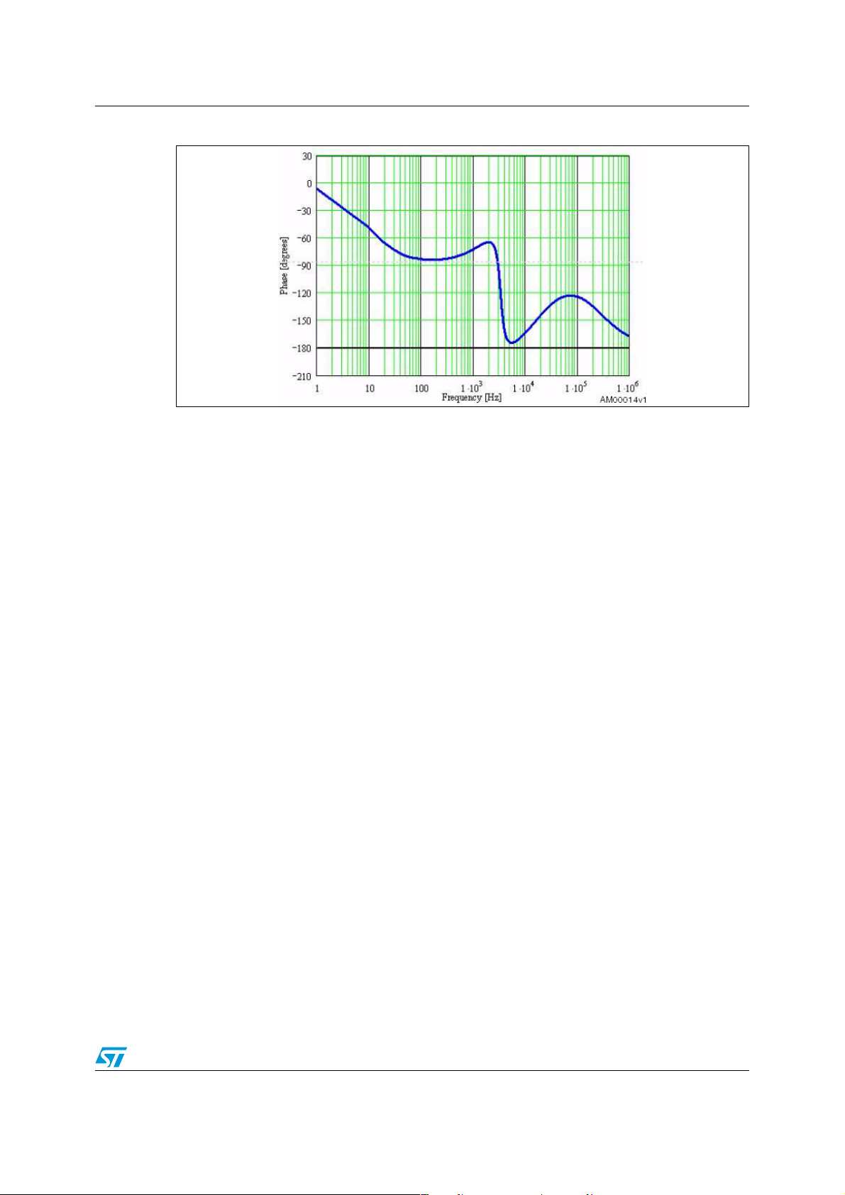
AN1517 Closing the loop
Figure 12. Phase plot
The cut off frequency and the phase margin are:
Equation 16
FC22.8KHz=
Phase margin = 39.8°
15/29
Page 16

Application information AN1517
5 Application information
5.1 Component selection
5.1.1 Input capacitor
The input capacitor must be able to withstand the maximum input operating voltage and the
maximum RMS input current.
Since step-down converters draw current from the input in pulses, the input current is
squared and the height of each pulse is equal to the output current. The input capacitor has
to absorb all this switching current, which can be up to the load current divided by two (worst
case, with duty cycle of 50%). For this reason, the quality of these capacitors has to be very
high to minimize its power dissipation generated by the internal ESR, thereby improving
system reliability and efficiency. The critical parameter is usually the RMS current rating,
which must be higher than the RMS input current.
The maximum RMS input current (flowing through the input capacitor) is:
Equation 17
2
2
D
-------+
η
I
RMSIO
•=
----------------- -–
η
2D
•
D
Where η is the expected system efficiency, D is the duty cycle and I
the output DC current.
O
This function reaches its maximum value at D = 0.5 and the equivalent RMS current is equal
to I
divided by 2 (considering η = 1). The maximum and minimum duty cycles are:
O
Equation 18
V
------------------------------------------
V
INMINVSW
where V
D
MAX
is the freewheeling diode forward voltage and VSW the voltage drop across the
F
internal PDMOS. Considering the range D
I
going through the input capacitor. Capacitors that can be considered are:
RMS
● Electrolytic capacitors: These are widely used due to their low price and their
+
OUTVF
–
=
to D
MIN
D
MIN
, it is possible to determine the max
MAX
V
=and
--------------------------------------------
V
INMAXVSW
+
OUTVF
–
availability in a wide range of RMS current ratings. The only drawback is that,
considering ripple current rating requirements, they are physically larger than other
capacitors.
● Ceramic capacitors: If available for the required value and voltage rating, these
capacitors usually have a higher RMS current rating for a given physical dimension
(due to very low ESR). The drawback is the considerably high cost.
● Tantalum capacitor: Good, small tantalum capacitors with very low ESR are becoming
more available. However, they can occasionally burn if subjected to very high current
during charge. Therefore, it is better to avoid this type of capacitor for the input filter of
the device. They can, however, be subjected to high surge current when connected to
the power supply.
16/29
Page 17
AN1517 Application information
5.1.2 Output capacitor
The output capacitor is very important to meet the output voltage ripple requirement.
Using a small inductor value is useful to reduce the size of the choke but it increases the
current ripple. So, to reduce the output voltage ripple, a low ESR capacitor is required.
Nevertheless, the ESR of the output capacitor introduces a zero in the open loop gain,
which helps to increase the phase margin of the system.
If the zero goes to a very high frequency, its effect is negligible. For this reason, ceramic
capacitors and very low ESR capacitors in general should be avoided.
Tantalum and electrolytic capacitors are usually good for this purpose.
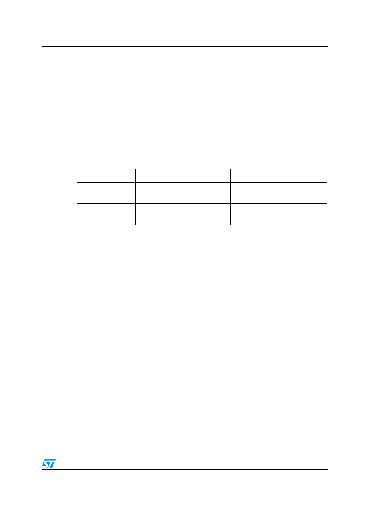
Ta bl e 3 below provides a list of some tantalum capacitor manufacturers.
Table 3. Recommended output capacitors
Manufacturer Series Cap value (µF) Rated voltage (V) ESR (mΩ)
AVX TPS 100 to 470 4 to 35 50 to 200
KEMET T494/5 100 to 470 4 to 20 30 to 200
Sanyo POSCAP
Sprague 595D 220 to 390 4 to 20 160 to 650
(1)
TPA/B/C 100 to 470 4 to 16 40 to 80
1. POSCAP capacitors have characteristic very similar to tantalum ones.
5.1.3 Inductor
The inductor value is very important because it fixes the ripple current flowing through
output capacitor.
The ripple current is usually fixed at 20-40% of I
A. The approximate inductor value is obtained using the following formula:
Equation 19
where T
For example, with V
21 µH.
The peak current through the inductor is given by:
Equation 20
and it can be observed that if the inductor value decreases, the peak current (which must be
lower than the current limit of the device) increases. So, when the peak current is fixed, a
higher inductor value allows a higher value for the output current.
ON
max, which is 0.3 - 0.6 A with IOmax = 1.5
O
V
–()
INVOUT
-------------------------------------- -
L
I∆
T
•=
ON
is the ON time of the internal switch, given by D · T.
= 3.3 V, VIN = 12 V and ∆IO = 0.45 A, the inductor value is about
OUT
I
PKIO
I∆
---- -+=
2
In Table 4: Inductor selection, some inductor manufacturers are listed.
17/29
Page 18
Application information AN1517
Table 4. Inductor selection
Manufacturer Series Inductor value (µH) Saturation current (A)
Coilcraft DO3316 33 to 47 1.6 to 2
Coiltronics UP2B 33 to 47 1.7 to 2
BI HM76-3 33 to 47 2 to 2.5
Epcos B82476 33 to 47 1.6 to 2
Wurth Elektronik 744561 33 to 47 1.6 to 2
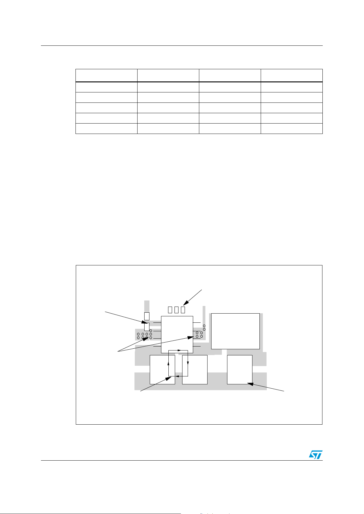
5.2 Layout considerations
The layout of switching DC-DC converters is very important to minimize noise and
interference. Power-generating portions of the layout are the main cause of noise and so
high switching current loop areas should be kept as small as possible and lead lengths as
short as possible.
High impedance paths (in particular the feedback connections) are susceptible to
interference, so they should be as far as possible from the high current paths. A layout
example is provided in Figure 13 below.
The input and output loops are minimized to avoid radiation and high frequency resonance
problems. The feedback pin connections to the external divider are very close to the device
to avoid pick-up noise. Moreover, the GND pin of the device is connected to the ground
plane directly with VIA on the bottom side of the PCB.
Figure 13. Layout example
COMPENSATION NETWORK FAR
FROM HIGH CURRENT PATHS
to output voltage
MINIMUN SIZE OF FEEDBACK
PIN CONNECTIONS TO AVOID
PICKUP
R2
45
CONNECTION TO
GROUNDPLANE
THROUGH VIAS
R1
L5972D
8
1
Vin Vout
L
Cin D Cout
Gnd
VERY SMALL HIGH CURRENT
CIRCULATING PATH TO MINIMIZE
RADIATION AND HIGH FREQUENCY
RESONANCE PROBL EMS
AM00131v1
OUTPUT CAPACITOR
DIRECTLY CONNECTED
TO HEAVY GROUND
18/29
Page 19

AN1517 Application information
5.3 Thermal considerations
The dissipated power of the device is tie to three different sources:
● switch losses due to the not negligible R
Equation 21
P
ON
R
DSONIOUT
where D is the duty cycle of the application. Note that the duty cycle is theoretically given by
the ratio between V
and VIN, but in practice it is substantially higher than this value to
OUT
compensate for the losses of the overall application. For this reason, the switching losses
related to the R
● Switching losses due to turning ON and OFF. These are derived using the following
increase compared to an ideal case.
DSON
equation:
Equation 22
T
+()
ONTOFF
P
SWVINIOUT
•
---------------------------------------- -
• FSW• VINI
2
. These are equal to:
DSON
()
• D•=
2
• TSW• FSW•==
OUT
Where T
current flowing into it during the turn ON and turn OFF phases. T
ON
and T
are the overlap times of the voltage across the power switch and the
OFF
is the equivalent
SW
switching time.
● Quiescent current losses.
Equation 23
P
VINIQ•=
Q
where I
● Example:
R
DSON
is the quiescent current.
Q
–V
–V
–I
IN
OUT
OUT
= 5 V
= 3.3 V
= 1.5 A
has a typical value of 0.25 Ω @ 25 °C and increases up to a maximum value of 0.5 Ω
@ 150 °C. We can consider a value of 0.4 Ω.
T
is approximately 70 ns. IQ has a typical value of 2.5 mA @ VIN = 12 V. The overall
SW
losses are:
Equation 24
P
TOT
R
DSONIOUT
0.4 1.520.7 51.570109–250 10352.5103–0.9W≅⋅⋅+⋅⋅⋅ ⋅ ⋅+⋅⋅=
()2DVINI
OUTTSWFSWVINIQ
=⋅+⋅⋅⋅+⋅⋅=
The junction temperature of device will be:
Equation 25
T
JTA
Where T
is the ambient temperature and Rth
A
ambient.
Rth
+=
P•
JA–
J-A
TOT
is the thermal resistance junction-to-
19/29
Page 20

Application information AN1517
Considering that the device in SO-8 (4+2+2) package mounted on board with a good
groundplane has a thermal resistance junction to ambient (Rth
) of about 62 °C/W and
J-A
considering an ambient temperature of about 70 °C.
Equation 26
TJ70 0.9 62 128°C≅•+=
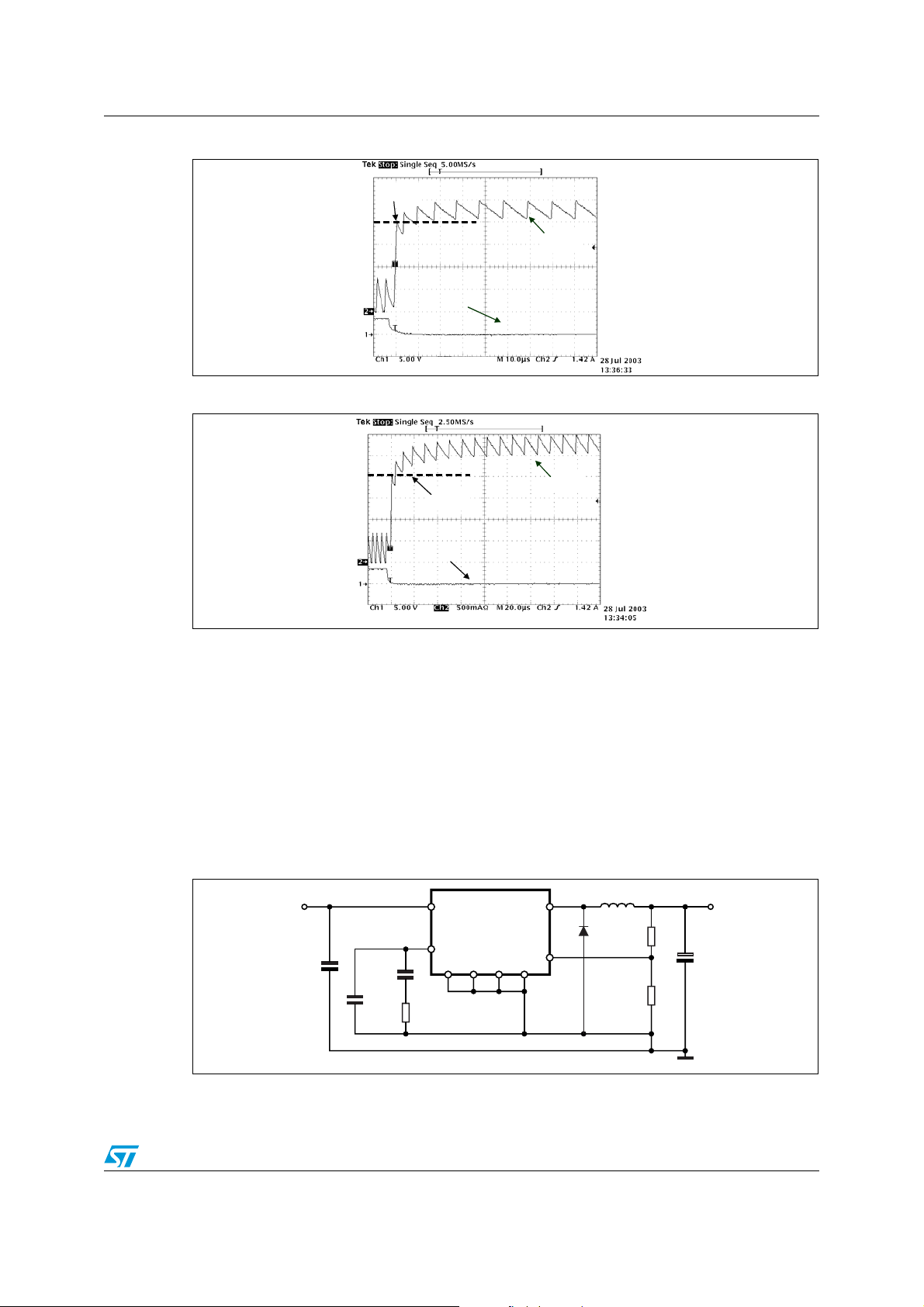
5.4 Short-circuit protection
In over-current protection mode, when the peak current reaches the current limit, the device
reduces the T
frequency to approximately one third of its nominal value (see Section 2.4: Current
protection). In these conditions, the duty cycle is strongly reduced and, in most applications,
this is enough to limit the current to I
output (V
OUT
effect of external components), the current peak could reach values higher than I
This can be understood considering the inductor current ripple during the ON and OFF
phases:
● ON phase
down to its minimum value (approximately 250 ns) and the switching
ON
. In any event, in case of heavy short-circuit at the
LIM
=0 V) and depending on the application conditions (VCC value and parasitic
.
LIM
Equation 27
•––()
DCRLI
T
•=
ON
● OFF phase
VINV
-------------------------------------------------------------------- -
IL∆
out
L
Equation 28
where V
VDV
------------------------------------------------------------------
IL∆
is the voltage drop across the diode, and DCRL is the series resistance of the
D
out
L
DCR
I•++()
L
T
•=
OFF
inductor.
In short-circuit conditions V
is negligible. So, during the T
OUT
, the voltage applied to the
OFF
inductor is very small and it may be that the current ripple in this phase does not
compensate for the current ripple during the T
The maximum current peak can be easily measured through the inductor with V
(short-circuit) and V
CC=VIN
max. In cases where the application must sustain the short-
ON
.
= 0 V
OUT
circuit condition for an extended period, the external components (mainly the inductor and
diode) must be selected based on this value.
20/29
Page 21
AN1517 Application information
Figure 14. Short-circuit current VIN = 25 V
I
LIMIT
I
Vout
Figure 15. Short-circuit current V
In Figure 14 and Figure 15, for example, it can be observed that when the input voltage
increases for a given component list, the current peak increases also. The current limit is
immediately triggered but the current peak increases until the current ripple during the T
is equal to the current ripple during the T
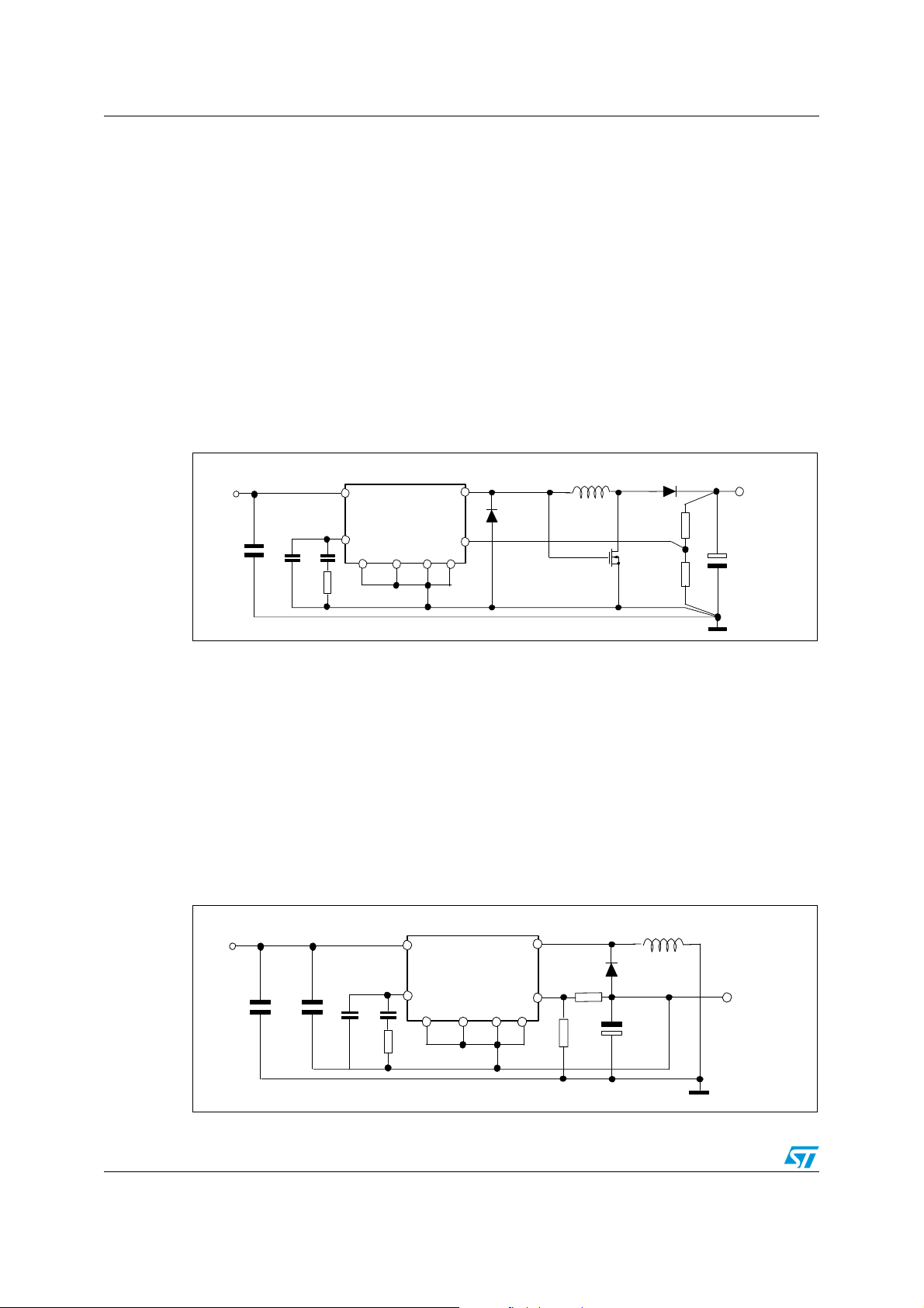
5.5 Application circuit
Figure 16 shows the demonstration board application circuit for the device in the SMD
version, where the input supply voltage, V
voltage of the input capacitor and the output voltage is adjustable from 1.235 V to V
I
LIMIT
Vout
= 30 V
IN
I
.
ON
, can range from 4.4 V to 25 V due to the rated
CC
CC
.
OFF
Figure 16. Demonstration board application circuit
VIN = 4.4V to 25V
C1
10µF
25V
CERAMIC
VCC OUT
8
4
6
L5972D
2
3
C4
22nF
C3
220pF
COMP
R3
4.7K
7
1
5
GND
FB
AM00027v1
L1 33µH
D1
STPS2L25U
R1
5.6K
R2
3.3K
VOUT=3.3V
C2
100µF
10V
21/29
Page 22

Application information AN1517
Table 5. Component list
Reference Part number Description Manufacturer
C1 10 µF, 25 V Tokin
C2 POSCAP 10TPB100M 100 µF, 10 V Sanyo
C3 C1206C221J5GAC 220 pF, 5%, 50 V KEMET
C4 C1206C223K5RAC 22 nF, 10%, 50 V KEMET
R1 5.6 K, 1%, 0.1 W 0603 Neohm
R2 3.3 K, 1%, 0.1 W 0603 Neohm
R3 4.7 K, 1%, 0.1 W 0603 Neohm
D1 STPS2L25U 2 A, 25 V STMicroelectronics
L1 DO3316P-333 33 µH, 2.1 A Coilcraft
Figure 17. PCB layout (component side)
42mm
AM00132v1
Figure 18. PCB layout (bottom side)
22/29
34mm
AM00133v1
Page 23

AN1517 Application information
Figure 19. PCB layout (front side)
AM00134v1
Below are some graphs showing the T
versus output current in different input and output
j
voltage conditions.
Figure 20. Junction temperature vs. output
TJ(°C)
100.0
90.0
80.0
70.0
60.0
50.0
40.0
30.0
20.0
current
Vin=5V
Tamb.=25°C
0.2 0.4 0.6 0.8 1 1.2 1.4 1.6 1.8 2
Io(A)
Vo=2.5V
Vo=3.3V
Vo=1.8V
Figure 22. Junction temperature vs. output
current
95
93
91
89
87
85
83
81
79
77
Efficiency (%)
75
73
Vin=5V
71
69
67
0.1 0.3 0.5 0.7 0.9 1.1 1.3 1.5 1.7
Vo=1.8V
Vo=1.8V
Vo=2.5V
Vo=2.5V
Vo=3.3V
Vo=3.3V
Io (A)
Figure 21. Junction temperature vs. output
current
TJ(°C)
100.0
90.0
Vin=12V
80.0
70.0
60.0
50.0
40.0
30.0
20.0
Tamb= 25°C
0.2 0.4 0.6 0.8 1 1.2 1.4 1 .6 1.8 2
Io(A)
Vo=5V
Vo=2.5V
Vo=3.3V
Figure 23. Efficiency vs. output current
96
94
92
90
88
86
84
82
80
Efficiency (%)
78
76
74
Vin=12V
Vin=12V
72
70
0.1 0.3 0.5 0.7 0.9 1.1 1.3 1.5 1.7
Vo=3.3V
Vo=3.3V
Vo=2.5V
Vo=2.5V
Vo=5V
Vo=5V
Io (A)
23/29
Page 24
Application ideas AN1517
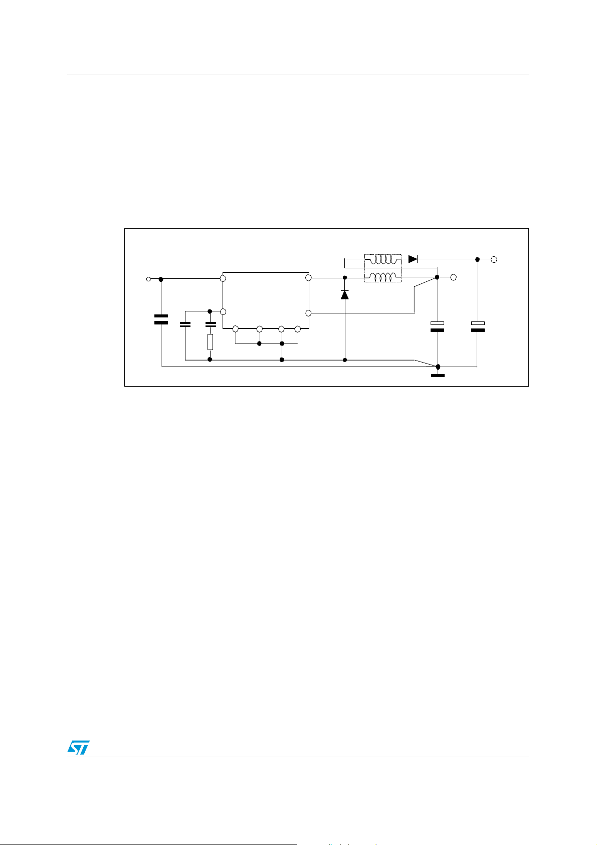
6 Application ideas
6.1 Positive buck-boost regulator
The device can be used to implement an step-up/down converter with a positive output
voltage. Figure 24 below shows the schematic diagram of this topology for an output voltage
of 12 V.
The input voltage can range from 5 V and 35 V. The output voltage is given by V
D/(1-D), where D is the duty cycle. The maximum output current is given by I
The current capability is reduced by the term (1-D) and so, for example, with a duty cycle of
0.5, the maximum output current deliverable to the load is 0.75 A. This is due to the fact that
the current flowing through the internal power switch is delivered to the output only during
the OFF phase.
Figure 24. Positive buck-boost regulator
C3
22nF
R3
4.7k
Vcc
COMP
8
L5972D
4
2
7
6
GND
VIN=5V
C1
10uF
10V
Ceramic
C2
220pF
7 Buck-boost regulator
·
O=VIN
=1× (1-D).
OUT
L1
OUT
1
5
3
FB
D1
STPS2L25U
33uH
AM00136v1
D2
STPS2L2 5U
M1
STN4NE03L
24k
2.7k
VOUT=1 2V/0.45A
C4
100uF
16V
In Figure 25, the schematic circuit for a standard buck-boost topology is shown. The output
voltage is given by V
= -VIN · D/(1-D). The maximum output current is equal to I
O
D), for the same reason as that of the up-down converter. An important thing to take in
account is that the ground pin of the device is connected to the negative output voltage.
Therefore, the device is subjected to a voltage equal to V
36 V (the maximum operating input voltage).
Figure 25. Buck-boost regulator
C4
22nF
R3
4.7k
Vcc
COMP
8
L5972D
4
2
VIN=5V
C1
10uF
10V
Ceramic
C2
10uF
25V
Ceramic
C3
220pF
24/29
=1 · (1-
OUT
, which has to be lower than
IN-VO
L1
OUT
33uH
1
D1
2.7k
AM00135v1
STPS2L25U
C5
100uF
16V
VOUT=-12V/0.45A
FB
5
6
GND
3
7
24k
Page 25
AN1517 Buck-boost regulator
7.1 Dual output voltage with auxiliary winding
When two output voltages are required, it is possible to create a dual output voltage
converter by using a coupled inductor. During the ON phase the current is delivered to V
while D2 is reverse-biased.
During the OFF phase, the current is delivered through the auxiliary winding to the output
voltage V
. This is possible only if the magnetic core has stored sufficient energy. So, to
OUT1
be certain that the application is working properly, the load related to the second output
V
should be much lower than the load related to V
OUT1
OUT
.
Figure 26. Dual output voltage with auxiliary winding
OUT
VIN=12V
C1
10uF
25V
C2
220pF
C3
22nF
R3
4.7k
Vcc
COMP
n=N1/N2=2
8
L5972D
4
6
2
7
GND
OUT
1
D1
FB
5
STPS2L25U
3
AM00137v1
N2
N1
D2
STPS2L25U
VOUT=3.3V
C4
100uF
10V
VOUT1=5V
50mA
C5
47uF
10V
25/29
Page 26

Compensation network with MLCC (multiple layer ceramic capacitor) at the output AN1517
8 Compensation network with MLCC (multiple layer
ceramic capacitor) at the output
MLCCs with values in the range of 10 µF-22 µF and rated voltages in the range of 10 V-25 V
are available today at relatively low cost from many manufacturers.
These capacitors have very low ESR values (a few mΩ) and thus are occasionally used for
the output filter in order to reduce the voltage ripple and the overall size of the application.
However, a very low ESR value affects the compensation of the loop (see Section 4: Closing
the loop) and in order to keep the system stable, a more complicated compensation network
may be required. Figure 27 shows an example of compensation network that stabilizes the
system with ceramic capacitors at the output (the optimum component value depends on
the application).
Figure 27. MLCC compensation network example
4.7uH
4.7uH
Coilcraft
VIN=5V
VIN=5V
C1
C1
MLCC
MLCC
10uF
10uF
C3=220pF
C3=220pF
C4=4.7 nF
C4=4.7 nF
Vcc
Vcc
COMP
COMP
R3=2.2K
R3=2.2K
OUT
37
37
1
1
5
5
GND
GND
OUT
FB
FB
D1
D1
8
8
L5972D
L5972D
4
4
6
6
2
2
Coilcraft
STPS2 L25U
STPS2 L25U
L1
L1
VOUT=2.1V
VOUT=2.1V
C2
C2
MLCC
MLCC
22uF
22uF
6.3V
6.3V
R4=47 0
R2=4K7
R2=4K7
R1=3.3K
R1=3.3K
R4=47 0
C5=2.7 nF
C5=2.7 nF
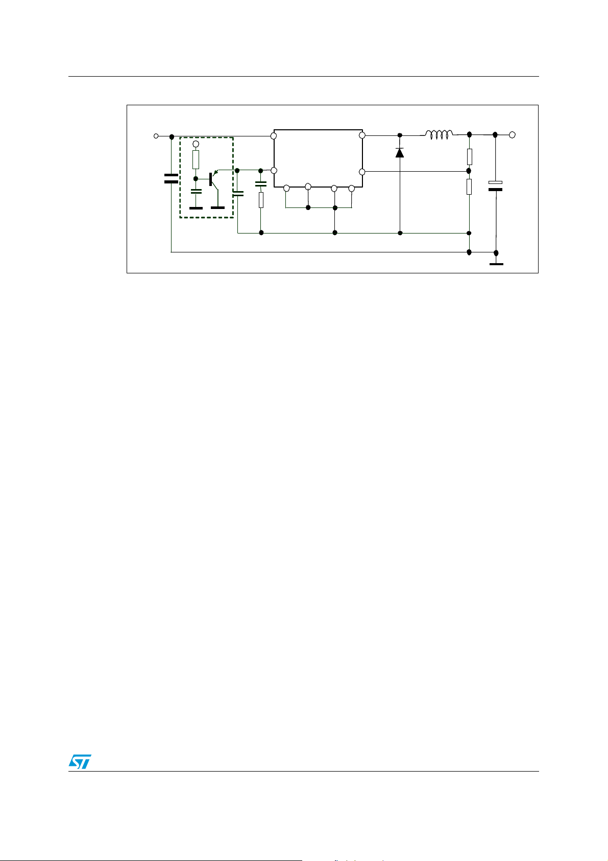
8.1 External soft-start network
At the start-up, the device can quickly increase the current up to the current limit in order to
charge the output capacitor. If a soft ramp-up of the output voltage is required, an external
soft-start network can be implemented as shown in Figure 28. The capacitor C is charged
up to an external reference (through R), and the B
This clamps the duty cycle, limiting the slew rate of the output voltage.
AM00138v1
clamps the COMP pin.
JT
26/29
Page 27
AN1517 Compensation network with MLCC (multiple layer ceramic capacitor) at the output
Figure 28. Soft-start network example
33uH
33uH
Coilcraft
VIN=4.4V to 25V
VIN=4.4V to 25V
C1
C1
10uF
10uF
25V
25V
CERAMIC
CERAMIC
VREF
VREF
VREF
R=4K7
R=4K7
R=4K7
Css=2.7nF
Css=2.7nF
BC327
BC327
C4=22nF
C4=22nF
C3=220pF
C3=220pF
Vcc
Vcc
COMP
COMP
R3=4.7K
R3=4.7K
OUT
3
3
1
1
5
5
GND
GND
OUT
FB
FB
D1
D1
8
8
L5972D
L5972D
4
4
6
6
2
2
7
7
Coilcraft
STPS2L25U
STPS2L25U
L1
L1
R2=3.3K
R2=3.3K
AM00139v1
VOUT=3.3V
VOUT=3.3V
R1=5.6K
R1=5.6K
C2
C2
100uF
100uF
10V
10V
27/29
Page 28

Revision history AN1517
9 Revision history
Table 6. Document revision history
Date Revision Changes
08-Nov-2006 1 First issue
– The document has been reformatted
28-May-2007 2
– Section 4: Closing the loop modified
– Minor text changes
28/29
Page 29

AN1517
Please Read Carefully:
Information in this document is provided solely in connection with ST products. STMicroelectronics NV and its subsidiaries (“ST”) reserve the
right to make changes, corrections, modifications or improvements, to this document, and the products and services described herein at any
time, without notice.
All ST products are sold pursuant to ST’s terms and conditions of sale.
Purchasers are solely responsible for the choice, selection and use of the ST products and services described herein, and ST assumes no
liability whatsoever relating to the choice, selection or use of the ST products and services described herein.
No license, express or implied, by estoppel or otherwise, to any intellectual property rights is granted under this document. If any part of this
document refers to any third party products or services it shall not be deemed a license grant by ST for the use of such third party products
or services, or any intellectual property contained therein or considered as a warranty covering the use in any manner whatsoever of such
third party products or services or any intellectual property contained therein.
UNLESS OTHERWISE SET FORTH IN ST’S TERMS AND CONDITIONS OF SALE ST DISCLAIMS ANY EXPRESS OR IMPLIED
WARRANTY WITH RESPECT TO THE USE AND/OR SALE OF ST PRODUCTS INCLUDING WITHOUT LIMITATION IMPLIED
WARRANTIES OF MERCHANTABILITY, FITNESS FOR A PARTICULAR PURPOSE (AND THEIR EQUIVALENTS UNDER THE LAWS
OF ANY JURISDICTION), OR INFRINGEMENT OF ANY PATENT, COPYRIGHT OR OTHER INTELLECTUAL PROPERTY RIGHT.
UNLESS EXPRESSLY APPROVED IN WRITING BY AN AUTHORIZED ST REPRESENTATIVE, ST PRODUCTS ARE NOT
RECOMMENDED, AUTHORIZED OR WARRANTED FOR USE IN MILITARY, AIR CRAFT, SPACE, LIFE SAVING, OR LIFE SUSTAINING
APPLICATIONS, NOR IN PRODUCTS OR SYSTEMS WHERE FAILURE OR MALFUNCTION MAY RESULT IN PERSONAL INJURY,
DEATH, OR SEVERE PROPERTY OR ENVIRONMENTAL DAMAGE. ST PRODUCTS WHICH ARE NOT SPECIFIED AS "AUTOMOTIVE
GRADE" MAY ONLY BE USED IN AUTOMOTIVE APPLICATIONS AT USER’S OWN RISK.
Resale of ST products with provisions different from the statements and/or technical features set forth in this document shall immediately void
any warranty granted by ST for the ST product or service described herein and shall not create or extend in any manner whatsoever, any
liability of ST.
ST and the ST logo are trademarks or registered trademarks of ST in various countries.
Information in this document supersedes and replaces all information previously supplied.
The ST logo is a registered trademark of STMicroelectronics. All other names are the property of their respective owners.
© 2008 STMicroelectronics - All rights reserved
STMicroelectronics group of companies
Australia - Belgium - Brazil - Canada - China - Czech Republic - Finland - France - Germany - Hong Kong - India - Israel - Italy - Japan -
Malaysia - Malta - Morocco - Singapore - Spain - Sweden - Switzerland - United Kingdom - United States of America
www.st.com
29/29
 Loading...