

Page 1

AN1514
Application note
VIPower: double output buck or
buck-boost converter using VIPer12A-E/22A-E
Introduction
This paper introduces two double output off-line non isolated SMPS based on the
VIPerX2A-E family. The first SMPS is a Buck converter with two positive outputs and the
second one is a Buck-Boost converter with two negative outputs. The use of VIPer12A-E or
VIPer22A-E in both converters depends on the output power specifications. The power
supplies are operated in off-line mode with an extended wide range of the input voltage,
from 80 to 285 Vac. The target applications are small loads, such as microcontrollers,
motors, displays and peripherals in several industrial and home appliances.
Two converter topologies are introduced in this paper. The considered double output
converters are based on the VIPerX2A-E device family and are suitable for non isolated offline applications. VIPerX2A-E is a low cost monolithic smart power with a PWM controller,
start-up circuit and protection integrated on the same chip. The power stage consists of a
vertical Power MOSFET with 730 V breakdown voltage and 0.32 A for VIPer12A-E or 0.56 A
for VIPer22A-E maximum drain current with internal limitation.
The use of a VIPower device makes the design very simple and easy, since several features
are integrated in the smart power IC. The first SMPS is a Buck converter with two positive
outputs and the second one is a Buck-Boost converter with two negative outputs. The use of
VIPer12A-E or VIPer22A-E in both converters depends on the output power specifications.
The power supplies are operated in off-line mode with an extended wide range of the input
voltage, from 80 to 285 Vac.
The target applications are small loads, such as microcontrollers, motors, displays and
peripherals in several industrial and home appliances with power level up to 6-8 W.
September 2007 Rev 2 1/17
www.st.com
Page 2

Contents AN1514
Contents
1 Off-line double output converters . . . . . . . . . . . . . . . . . . . . . . . . . . . . . . 5
2 VIPer application examples . . . . . . . . . . . . . . . . . . . . . . . . . . . . . . . . . . . 5
2.1 Double output buck converter using VIPer12A-E . . . . . . . . . . . . . . . . . . . . 6
2.1.1 Experimental results . . . . . . . . . . . . . . . . . . . . . . . . . . . . . . . . . . . . . . . . 8
2.2 Double output buck-boost converter using VIPer22A-E . . . . . . . . . . . . . . . 9
2.2.1 Experimental results . . . . . . . . . . . . . . . . . . . . . . . . . . . . . . . . . . . . . . . 11
2.2.2 Thermal measurements . . . . . . . . . . . . . . . . . . . . . . . . . . . . . . . . . . . . . 12
3 Conclusion . . . . . . . . . . . . . . . . . . . . . . . . . . . . . . . . . . . . . . . . . . . . . . . . 16
4 Revision history . . . . . . . . . . . . . . . . . . . . . . . . . . . . . . . . . . . . . . . . . . . 16
2/17
Page 3

AN1514 List of tables
List of tables
Table 1. Buck converter specifications . . . . . . . . . . . . . . . . . . . . . . . . . . . . . . . . . . . . . . . . . . . . . . . . 6
Table 2. Component list . . . . . . . . . . . . . . . . . . . . . . . . . . . . . . . . . . . . . . . . . . . . . . . . . . . . . . . . . . . 7
Table 3. Load regulation at V
Table 4. Load regulation at V
Table 5. Buck-boost converter specifications . . . . . . . . . . . . . . . . . . . . . . . . . . . . . . . . . . . . . . . . . . 10
Table 6. Component list . . . . . . . . . . . . . . . . . . . . . . . . . . . . . . . . . . . . . . . . . . . . . . . . . . . . . . . . . . 11
Table 7. Load regulation at V
Table 8. Load regulation at V
Table 9. Thermal characterization (package: DIP8; R
T
=25°C). . . . . . . . . . . . . . . . . . . . . . . . . . . . . . . . . . . . . . . . . . . . . . . . . . . . . . . . . . . . . 14
amb
Table 10. Document revision history . . . . . . . . . . . . . . . . . . . . . . . . . . . . . . . . . . . . . . . . . . . . . . . . . 16
=80V
in
=285V
in
=80V
in
=285V
in
. . . . . . . . . . . . . . . . . . . . . . . . . . . . . . . . . . . . . . . . . . . . . . 9
acrms
. . . . . . . . . . . . . . . . . . . . . . . . . . . . . . . . . . . . . . . . . . . . . 9
acrms
. . . . . . . . . . . . . . . . . . . . . . . . . . . . . . . . . . . . . . . . . . . . . 11
acrms
. . . . . . . . . . . . . . . . . . . . . . . . . . . . . . . . . . . . . . . . . . . . 12
acrms
=45°C/W mounted by socket;
thj-lead
3/17
Page 4

List of figures AN1514
List of figures
Figure 1. Double output buck topology . . . . . . . . . . . . . . . . . . . . . . . . . . . . . . . . . . . . . . . . . . . . . . . . 5
Figure 2. Double output buck-boost topology . . . . . . . . . . . . . . . . . . . . . . . . . . . . . . . . . . . . . . . . . . . 5
Figure 3. Converter schematic . . . . . . . . . . . . . . . . . . . . . . . . . . . . . . . . . . . . . . . . . . . . . . . . . . . . . . . 6
Figure 4. Board layout . . . . . . . . . . . . . . . . . . . . . . . . . . . . . . . . . . . . . . . . . . . . . . . . . . . . . . . . . . . . . 8
Figure 5. Board prototype . . . . . . . . . . . . . . . . . . . . . . . . . . . . . . . . . . . . . . . . . . . . . . . . . . . . . . . . . . 8
Figure 6. Efficiency vs. output power . . . . . . . . . . . . . . . . . . . . . . . . . . . . . . . . . . . . . . . . . . . . . . . . . . 9
Figure 7. Converter schematic . . . . . . . . . . . . . . . . . . . . . . . . . . . . . . . . . . . . . . . . . . . . . . . . . . . . . . 10
Figure 8. Efficiency vs. output power . . . . . . . . . . . . . . . . . . . . . . . . . . . . . . . . . . . . . . . . . . . . . . . . . 12
Figure 9. V
Figure 10. V
Figure 11. VIPer22A-E temperature at maximum load with parasitic capacitance . . . . . . . . . . . . . . . 13
Figure 12. V
Figure 13. Conducted emissions at full load with EN55014 limits: line emissions. . . . . . . . . . . . . . . . 15
Figure 14. Conducted emissions at full load with EN55014 limits: neutral emissions . . . . . . . . . . . . . 15
=80V
in
=285V
in
and ID at Vin=230V
DS
acrms
acrms
, I
out2
, I
out2
=75 mA, CH1=V
=75 mA, CH1=V
, I
acrms
=250 mA . . . . . . . . . . . . . . . . . . . . . . . . . . . . . . . . . . . . . 14
out
out1
out1
, CH2=I
, CH2=I
, CH3=ILp, CH4=V
out1
, CH3=ILp, CH4=V
out1
. . . . . . . . . . . . . 13
out2
. . . . . . . . . . . . 13
out2
4/17
Page 5
AN1514 Off-line double output converters
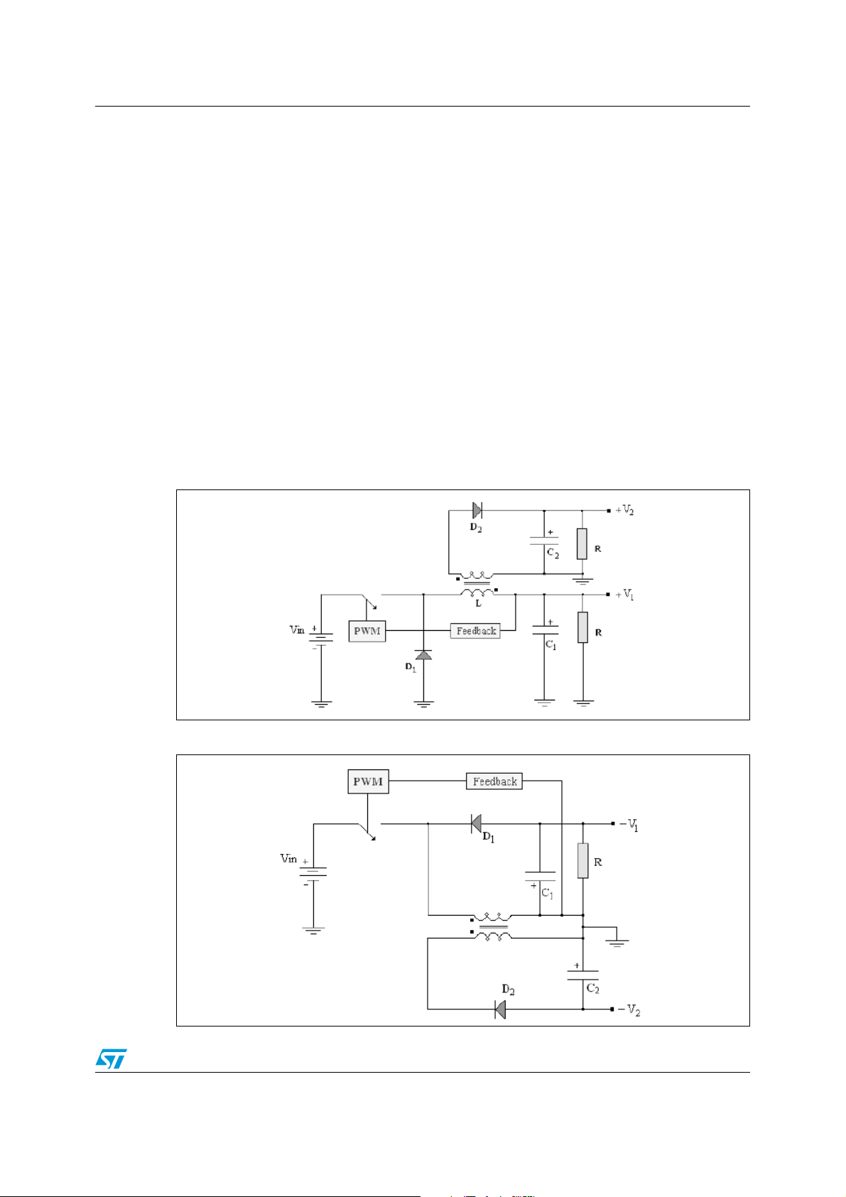
1 Off-line double output converters
In these circuits the first output is obtained using the standard buck or buck-boost topology,
while the second output is obtained by means of a second winding on the main inductor.
This output is directly coupled with the first one in flyback mode and its value is given by the
turns ratio n. The inductor is still low cost since a drum core can be used and the coupling
between the two windings is not as critical as in a flyback converter. The electrical
schematics of both configurations are shown in Figure 1 and Figure 2.
2 VIPer application examples
In this section two VIPerX2A-E application examples are introduced:
1. Double output buck converter 24 V at 30 mA, 5 V at 50 mA
2. Double output buck-boost converter (-24 V) at 250 mA, (-5 V) at 70 mA.
Figure 1. Double output buck topology
Figure 2. Double output buck-boost topology
5/17
Page 6
VIPer application examples AN1514
2.1 Double output buck converter using VIPer12A-E
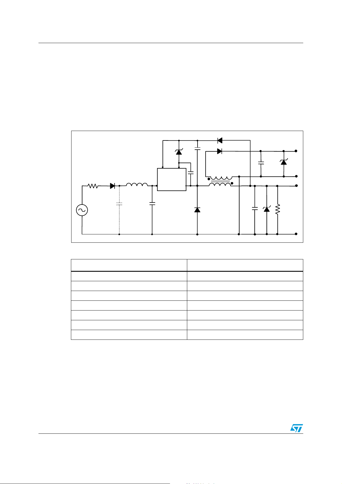
The proposed power supply, shown in Figure 3, is based on VIPer12A-E. The specifications
of the converter are listed in Ta b le 1 . The input section consists of a resistor as a fuse, a
single diode rectifier, and an input LC filter. Such a filter provides both DC voltage
stabilization and improved EMI performance (compliant with EN55022 Class B standard).
The capacitor Cin1 could be connected to provide further reduction of conducted EMI, if
required.
The switching frequency is 60 kHz, given by the integrated oscillator of the VIPer12A-E.
Figure 3. Converter schematic
D
3
D
z
C
3
D
2
V
FB
dd
D
R
f
r
L
f
VIPer12A-E
D
C
4
S
n
C
D
2
L
V
AC
C
in1
C
in
D
1
C
1
D
z1
+5V
z2
V
out2
+24V
V
out1
R
burden
GND
Table 1. Buck converter specifications
Parameter Value
AC input voltage V
Output current I
Output current I
Output voltage V
Output voltage V
inac
out
out2
out1
out2
80 - 285 Vac
30 mA
50 mA
+24±10%V
+5 V±5%
Switching frequency 60 kHz
Output power ~ 1 W
The two outputs are provided using a buck converter for the 24 V output, named "V
a coupled inductor in flyback mode for the 5 V output, named "V
feedback is connected to "V
" as well as the supply circuit of the VIPer12A-E. Doing so,
out1
". The regulation
out2
out1
", and
only one high voltage diode and one capacitor are needed, i.e. D3 and C3 in Figure 3,
reducing the complexity and the cost of the circuit.
The output inductor, L, has two coupled windings on the same ferrite core, with a proper turn
ratio and coupling factor in order to get the correct output voltage. In particular, 1.5 mH
inductor is used, with N1=200t - wound on the ferrite core of "PANASONIC ELC10D152E"
inductor - and N2=60t. Zener diodes, Dz1 and Dz2 protect both outputs against overvoltage.
6/17
Page 7

AN1514 VIPer application examples
A burden resistor is connected across V
V
is in open load condition. Such a resistor greatly improves the regulation with a slight
out1
in order to perform the regulation on V
out1
out2
when
impact on the efficiency.
The output rectifier diodes are both fast diodes: D1 is a high voltage diode since it has to
sustain a reverse voltage given by the input DC bus voltage while D2 is a low voltage diode.
The part list of the proposed circuit is given in Tab le 2 . In Figure 4 the board layout is shown
and Figure 5 shows the lab prototype.
Table 2. Component list
Reference Value Description
R
r
R
f
Rburden 4.7 KΩ 1/4 W
C
in
C
1
C
2
C
3
C
4
D
r
D
1
D
2
D
3
D
Z
D
Z1
D
Z2
L 1.5 mH
10 Ω 1/2 W
10 KΩ 1/4 W
4.7 µF, 450 V Electrolytic capacitor
33 µF, 50 V Electrolytic capacitor
100 µF, 16 V Electrolytic capacitor
1 µF, 25 V Electrolytic capacitor
22 nF Ceramic capacitor
Diode 1N4007
Diode BA159 (fast)
Diode 1N4148 (fast)
Diode 1N4004
22 V Zener
27 V Zener
5.6 V Zener
L
f
470 µH Inductor
IC1 STMicroelectronics VIPer12A-E
7/17
Page 8

VIPer application examples AN1514
Figure 4. Board layout
Figure 5. Board prototype
2.1.1 Experimental results
In this section the characterization of the circuit is given. Four load conditions have been
considered:
1. Output1 = open load - output2 = open load
2. Output1 = full load - output2 = open load
3. Output1 = open load - output2 = full load
4. Output1 = full load - output2 = full load
In Ta bl e 3 and Tabl e 4 the experimental results are listed, with 80 V and 285 V input voltage
respectively. In all the considered operating conditions the proposed power supply meets
the given specifications. The efficiency has been evaluated and is shown in Figure 6, where
the output power P
Equation 1
8/17
is given by (Equation 1).
out
P
outPout1Pout2
+=
Page 9

AN1514 VIPer application examples
Table 3. Load regulation at V
Vin=80Vac V
1 24.95 5 5.58 0
2 26.16 30 5.58 0
3 26.98 5 4.90 50
4 24.02 30 5.06 50
(V) I
out1
Table 4. Load regulation at Vin=285V
Vin=285Vac Vout1(V) Iout1(mA) Vout2(V) Iout2(mA)
1 24.95 5 5.58 0
2 24.39 30 5.58 0
3 24.86 5 4.75 50
4 24.39 30 5.20 50
=80V
in
acrms
(mA) V
out1
acrms
(V) I
out2
Figure 6. Efficiency vs. output power
out2
(mA)
2.2 Double output buck-boost converter using VIPer22A-E
The proposed power supply, shown in Figure 7, is based on VIPer22A-E. It delivers
maximum 7 W output power in wide range, according to Ta bl e 5 which lists the main
specifications of the converter. This topology is used to supply negative output voltage
referred to neutral in non isolated applications. The input stage is similar to the Buck based
application but requires a larger bulk capacitor due to the higher power level, as shown in
Ta bl e 6 .
9/17
Page 10

VIPer application examples AN1514
Table 5. Buck-boost converter specifications
Parameter Value
AC input voltage V
Output current I
Output current I
Output voltage V
Output voltage V
Switching frequency 60 kHz
Output power ~ 7 W
inac
250 mA
out1
out2
-24±10%V
out1
out2
80 - 285 Vac
70 mA
-5 V±5%
The two outputs are provided using a Buck-Boost converter for the -24 V output, named
"V
", and a coupled inductor in flyback mode for the -5 V output, named "V
out1
regulation feedback is connected to "V
" as well as the supply circuit of the Viper22A-E.
out1
out2
". The
Doing so, only one high voltage diode and one capacitor are needed, i.e. D2 and C3 in
Figure 7, reducing the complexity and the cost of the circuit.
The output inductor, L, has two coupled windings on the same ferrite core, with a proper turn
ratio and coupling factor in order to get the correct output voltage. In particular, 1 mH
inductor "PANASONIC ELC08D102E" is used with a second winding (N2=45 turns) in order
to obtain the secondary output.
Zener diode Dz2 protects the Out2 against overvoltage, but this protection is not needed in
Out1. A burden resistor (R
) is connected across V
b
in order to perform the regulation on
out1
Vout2 when Vout1 is in open load condition. The output rectifier diodes are both ultrafast
diodes: D3 is a high voltage diode since it has to sustain a reverse voltage given by the input
DC bus voltage while D4 is a low voltage diode. The part list of the proposed circuit is given
in Ta bl e 6 .
Figure 7. Converter schematic
10/17
-E
Page 11

AN1514 VIPer application examples
Table 6. Component list
Reference Value Description
R
(Fuse) 10 Ω1/2 W
f
b 1.5 kΩ1/2 W
R
C
10 µF, 400 V Electrolytic capacitor
1
C
2
10 µF, 25 V Electrolytic capacitor
C
3
C
100 nF Ceramic capacitor
4
220 µF,16 V Electrolytic capacitor
C
5
220 µF,25 V Electrolytic capacitor
C
6
D
Diode 1N4007
1
Diode BYT400 (fast)
D
2
D
Diode STTA106 (Turbosw.)
3
Diode STTA102 (200V)
D
4
24V Zener
D
Z1
D
5.6V Zener
Z2
1mH
L
p
45 turns
L
s
IC1 STMicroelectronics VIPer22ADIP-E
10 µF, 400 V Electrolytic capacitor
2.2.1 Experimental results
In this section the characterization of the circuit is given. Four load conditions have been
considered:
1. Output1 = open load - output2 = open load
2. Output1 = full load - output2 = open load
3. Output1 = open load - output2 = full load
4. Output1 = full load - output2 = full load
The experimental results are listed in Tab le 7 and Tab le 8 , with 80 V and 285 V input voltage
respectively. In all the considered operating conditions the proposed power supply meets
the given specifications. The efficiency has been evaluated and is shown in Figure 8, where
the output power P
Table 7. Load regulation at Vin=80V
Vin=80Vac V
1 -24.72 10 - 4.85 0
2 -23.86 250 - 5.54 0
3 -24.7 10 - 4.59 70
4. -23.7 250 - 4.88 70
is given by (Equation 1).
out
out1
(V) I
acrms
(mA) V
out1
(V) I
out2
out2
(mA)
11/17
Page 12

VIPer application examples AN1514
Table 8. Load regulation at V
Vin=285Vac V
1 -24.67 10 - 4.98 0
2 -24.1 250 - 5.61 0
3 -24.7 10 - 4.62 70
4 -24 250 - 5.03 70
(V) I
out1
=285V
in
Figure 8. Efficiency vs. output power
acrms
(mA) V
out1
(V) I
out2
out2
(mA)
2.2.2 Thermal measurements
Due to the higher power level of such a non isolated converter, thermal constraints have to
be evaluated in order to allow proper system operation. The main issue is related to parasitic
effects that can lead to higher power dissipation in the device and consequently a higher
working temperature. For example, if a fast diode is used, the recovery of charge generates
a current spike in the device increasing the switching losses, as shown in Figure 9 and
Figure 10 for V
temperature as shown in Figure 11.
=80 V and Vin=285 V respectively. The device is forced to operate at high
in
12/17
Page 13

AN1514 VIPer application examples
Figure 9. Vin=80V
Figure 10. Vin=285V
acrms
acrms
, I
=75 mA, CH1=V
out2
, I
=75 mA, CH1=V
out2
out1
out1
, CH2=I
, CH2=I
, CH3=ILp, CH4=V
out1
, CH3=ILp, CH4=V
out1
out2
out2
Figure 11. VIPer22A-E temperature at maximum load with parasitic capacitance
13/17
Page 14

VIPer application examples AN1514
In this case the temperature of the device will be so high as to enable the thermal shutdown
in a few minutes. If an ultra fast diode is used under the previous load condition, thermal
measurements give lower temperature as listed in Tabl e 9 . In such a case the temperature
increase is below 40°C increasing the efficiency of the system and allowing proper operation
with ambient temperature up to 65°C with no heat sink.
The above considerations apply to other parasitic elements on the board, e.g. stray
capacitance of the inductor, as shown in Figure 12. In this case a good inductor helps to limit
the power dissipation in the device and then the operating temperature.
In Figure 13 and Figure 14 the EMI behavior of the power supply at full load is shown, using
a 50 LISN according to EN550014 standard, for line and neutral respectively. Although the
measurements have been performed using peak detector, the emission level is well below
the Quasi-Peak (QP) limit, complying with the previously mentioned standard.
Table 9. Thermal characterization (package: DIP8; R
V
(Vrms) Pdiss (W) ∆T (°C) T (°C)
inac
80 0.7 30.6 55.6°C
220 0.58 26.1 51.1
285 0.88 39 64°C
Figure 12. V
socket; T
and ID at Vin=230V
DS
amb
=25°C)
acrms
, I
out
=250 mA
=45 °C/W mounted by
thj-lead
14/17
Page 15

AN1514 VIPer application examples
Figure 13. Conducted emissions at full load with EN55014 limits: line emissions
Figure 14. Conducted emissions at full load with EN55014 limits: neutral emissions
15/17
Page 16

Conclusion AN1514
3 Conclusion
Very low cost power supplies based on STMicroelectronics VIPerX2A family have been
proposed for low power applications where two non isolated voltages are required. Two
application examples have been given with a full characterization. The converters show
good performances in terms of electrical behavior, size and cost, confirming the suitability to
industrial as well as home appliance applications of such a VIPower device.
4 Revision history
Table 10. Document revision history
Date Revision Changes
04-Jan-2005 1 Minor text changes
– The document has been reformatted
26-Sep-2007 2
– VIPer12A becomes VIPer12A-E
– VIPer22A becomes VIPer22A-E
– VIPer22ADIP becomes VIPer22ADIP-E
16/17
Page 17

AN1514
Please Read Carefully:
Information in this document is provided solely in connection with ST products. STMicroelectronics NV and its subsidiaries (“ST”) reserve the
right to make changes, corrections, modifications or improvements, to this document, and the products and services described herein at any
time, without notice.
All ST products are sold pursuant to ST’s terms and conditions of sale.
Purchasers are solely responsible for the choice, selection and use of the ST products and services described herein, and ST assumes no
liability whatsoever relating to the choice, selection or use of the ST products and services described herein.
No license, express or implied, by estoppel or otherwise, to any intellectual property rights is granted under this document. If any part of this
document refers to any third party products or services it shall not be deemed a license grant by ST for the use of such third party products
or services, or any intellectual property contained therein or considered as a warranty covering the use in any manner whatsoever of such
third party products or services or any intellectual property contained therein.
UNLESS OTHERWISE SET FORTH IN ST’S TERMS AND CONDITIONS OF SALE ST DISCLAIMS ANY EXPRESS OR IMPLIED
WARRANTY WITH RESPECT TO THE USE AND/OR SALE OF ST PRODUCTS INCLUDING WITHOUT LIMITATION IMPLIED
WARRANTIES OF MERCHANTABILITY, FITNESS FOR A PARTICULAR PURPOSE (AND THEIR EQUIVALENTS UNDER THE LAWS
OF ANY JURISDICTION), OR INFRINGEMENT OF ANY PATENT, COPYRIGHT OR OTHER INTELLECTUAL PROPERTY RIGHT.
UNLESS EXPRESSLY APPROVED IN WRITING BY AN AUTHORIZED ST REPRESENTATIVE, ST PRODUCTS ARE NOT
RECOMMENDED, AUTHORIZED OR WARRANTED FOR USE IN MILITARY, AIR CRAFT, SPACE, LIFE SAVING, OR LIFE SUSTAINING
APPLICATIONS, NOR IN PRODUCTS OR SYSTEMS WHERE FAILURE OR MALFUNCTION MAY RESULT IN PERSONAL INJURY,
DEATH, OR SEVERE PROPERTY OR ENVIRONMENTAL DAMAGE. ST PRODUCTS WHICH ARE NOT SPECIFIED AS "AUTOMOTIVE
GRADE" MAY ONLY BE USED IN AUTOMOTIVE APPLICATIONS AT USER’S OWN RISK.
Resale of ST products with provisions different from the statements and/or technical features set forth in this document shall immediately void
any warranty granted by ST for the ST product or service described herein and shall not create or extend in any manner whatsoever, any
liability of ST.
ST and the ST logo are trademarks or registered trademarks of ST in various countries.
Information in this document supersedes and replaces all information previously supplied.
The ST logo is a registered trademark of STMicroelectronics. All other names are the property of their respective owners.
© 2007 STMicroelectronics - All rights reserved
STMicroelectronics group of companies
Australia - Belgium - Brazil - Canada - China - Czech Republic - Finland - France - Germany - Hong Kong - India - Israel - Italy - Japan -
Malaysia - Malta - Morocco - Singapore - Spain - Sweden - Switzerland - United Kingdom - United States of America
www.st.com
17/17
 Loading...