

Page 1

AN1506
APPLICATION NOTE
A MOTOR DRIVES SYSTEM FOR
WHEELCHAIR APPLICATIONS
G. Belverde - C. Guastella - M. Melito - A. Raciti
1. ABSTRACT
This paper deals with a new conc ept applied in designing low-voltage power MOSFE Ts that are suitable
for high-current low-voltage converter application s. The layout of the proposed dev ice famil y overc om es
the traditional cell structure by a new strip-based geometry. They present interesting characteristics due
to the advanced de sign rules typical of VLS I processes and s trong reduction of the on-state resistance.
Further, the technology process allows a significant simplification of the silicon fabrication steps, thus
allowing to enhance the device ruggedness. The hig h current handling in switching conditions (up to
150A) with a breakdown voltage in the range betwe en 20-50V in a convenient pac kage solution gi ve the
correct answers to the low-voltage range switch applications. This paper starts with the description of the
main technology issues in comparison with that of standard devices, particularly focusing on the
innovations and the improved performances. Moreover, a detailed characterization of the MOSFET
behavior in a traditional test circuit as well as in an actual AC motor drive for wheel chair applications are
presented and discussed.
2. INTRODUCTION.
Higher efficiencies are expected nowadays in the field of power converters for battery-powered systems.
As industrial and commercial applications of these systems are increasing more and more (laptops,
portable equipment, home appliances, electric assisted bikes, electric sc ooters, wheel chairs, mobiles,
etc.), higher efficiencies become of major interest in order to meet the user requirem ents of long-lasting
behavior with the sam e bat tery cha rge. To do that, researchers have made dra matic efforts in designing
new converter structures, in increasing the converter switching freq uency and in conceiving innovative
power devices.
Generally speaking, battery powered systems require low-voltage switching devices (<100V). Power
MOSFET de vices domina te in thi s voltage range due to t heir attractive c haracteristics of high sw itching
speed and easy driving capability. On-state losses of MOSFETs are of major concern on their total power
loss balance, esp ecially in case of converters with low or medium sw itching frequency. Since on-state
losses depend on the drain-source resistance (R
modern MOSFETs are realized with a cell-based layout, which determines low on-state resistance. The
increase of the cell density allows to further reduce th e on-state resistance, thus increasing the current
capability per device area-unit. However, for today’ s state-of-the-art MOSFETs, ulterior reduction of the
on-state resistance by this conventional layout is impeded since this approach is reaching its own
physical limit [1]. The need of innovative approaches arises in order to overcome the limit of this
technology.
), which is strictly related to the structure design, many
on
January 2002
1/14
Page 2

AN1506 - APPLICATION NOTE
The strip-based layout is a new approach [2], which allows using a simplified process for implant ing the
body and isolating the poly silicon gate from the source. The new technology is very effective in
eliminating the limit o f the cell-base d layout, which relies on the capability to open smaller and smaller
windows on the poly silicon area in order to obtain greater cell-density figures. With the strip-based
layout, MOSFET devices show improved performances and a simpler manufacturing process. Moreover,
they benefit of the well-established and advanced design rules typical of VLSI processes. On-state
resistance values as low as 1.2mΩ can be reached, but the overall MOSFET design must account for the
best trade-off of a merit figure, which is the product of the on-state resistance and the gate charge values
(R
on QG
).
In this paper the main issues of the new technology are briefly recalled, and the device structure is
described and discussed. The static and dynamic characteristics of devi ces b elonging t o this new f am ily
of MOSFETs are presented and compared with those of more traditional ones. Conventional
experimental tests have bee n carried out a nd are discussed aiming to de termine the impact of turn on
and turn off energy loss [3]. A low-voltage battery-powered converter for wheel chairs is used as a
workbench for an application-oriented characterization. Some relevant tests are reported and discussed.
A detailed analysis is done on the conduction and switching losses and the thermal behavior in the actual
application.
3. MAIN TECHNOLOGY ISSUES OF STRIP-BASED MOSFET.
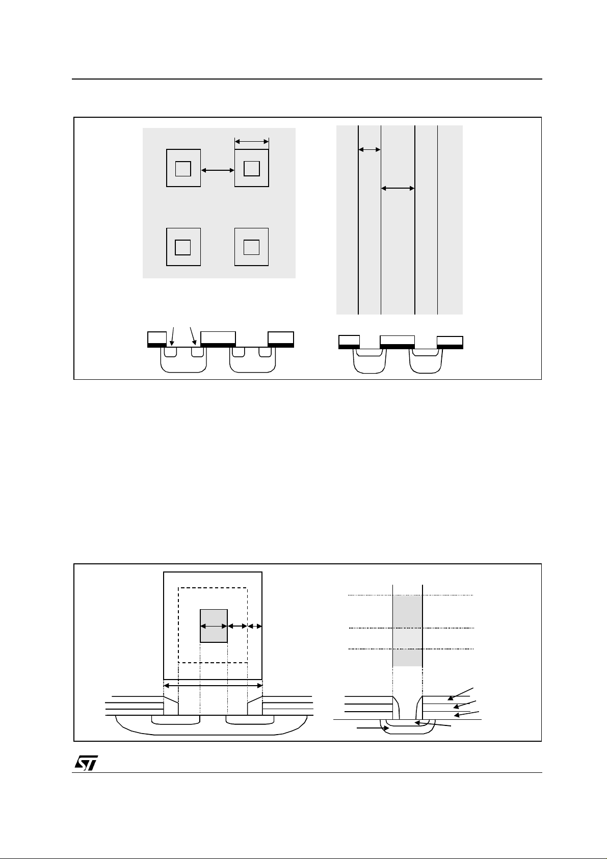
The structure of a strip-based MOSFET device overcomes the limit of a cell structur e. In figure 1 the
geometry of the t wo differently conceived devices are s hown. The m ain differences between a stan dard
square-cell layout and the strip imple mentation may be better unders tood by inspecting figure 2. In the
conventional cell structure shown, all subsequent contacts and isolation openings must be co nfined a nd
aligned inside the large st square windows opene d on the poly silicon layer whose side is L in fig ure 2.
That dimension depends on the alignment, the resolution, and the process tolerances and can be
expressed as:
Lc2b2t++=1()
where:
• c is the contact dimension for the body region imposed by the resolution of the photolithography
equipment;
• b is the contact dimension for the source re gion which depends on the alignm ent c apability and on the
metallization process;
• t is the separation (isolation) between the poly and sou rce metal and is controlled by the alignment
feature.
Consequently, the standard cell layout depends on three feature sizes.
2/14
Page 3
AN1506 - APPLICATION NOTE
Figure 1. Cell-based and strip-based structures of two Power MOSFETs
L
S
source
body
In the strip-based layout process an intermediate dielectric layer is obtained after growing the gate oxide
and depositing the poly silicon. In such a sandwich structure parallel strips are opened through an
appropriate photo masking process. After implanting the body, the source regions are created by using a
sort of small rectangle (patches) masking. The longer sides of the patches are perpendicular to the strips
in such a way that they do not need t o be aligned within the strip but only along their spacing, which
normally is larger than the opening, thus a voiding any alignment problem. Th e nex t s tep is to isolate the
poly silicon along the stripe’ s pe riphery thanks to the spacer proces s. Etching the dielectric material
originally deposited and creating “hills”on the sides of the strips achieve this. Finally, Aluminum
deposition is done in order to contact the strips, and the fabrication flow chart is completed.
L
S
source
body
Figure 2. Cell-based and strip-based structures of two Power MOSFETs showing the key
parameters of the elemental component of the geometry
a) b)
p
n
bt
c
L
cbt
source
body
source
p
n+
p
n+
p-vapox
poly
SiO2
n+
3/14
Page 4

AN1506 - APPLICATION NOTE
The source mask d oes not need to be aligned wit hin the strip itself; the only critical parameter is the
width of the strip (see figure 1), which depends on the equipm ent res olution. As can be argued from the
above description, the process benefits in a reduced number of feature sizes since it is now only
dependent on a single feature size, and higher packing dens ities can be obtained in comparison to the
conventional cell-geometry process. The new process is also named Extremely High Density (EHD)
referring to the possibility of getting devices with very high equivalent cell densities. Figure 3 compares
the obtainable channel perimeter density and thus the current density of the two structures.
Figure 3. Channel perimeter density comparison of cell-based and strip-based structures
30
]
2
25
20
Cell-based layout
Strip-based layout
15
Channel perimeter density [cm/mm
10
87654321
Minimum feature size [µm]
4. STATIC AND DYNAMIC BEHAVIOR OF THE NEW DEVICE.
The resulting MOSFET device of the strip-based process shows very interesting characteristics:
extremely high packing densit y and low on -state resistance, rugged aval anche charact eristics, and less
critical alignment steps. First of all we have selected the device STB8 0NF55, which was the cand idate
for the actual application in an AC drive. The drive is described with more details in the next section. The
main electrical quantities of the component are summarized in Table 1.
Table 1. STB80NF55 Main Electrical Characteristics
R
on
[mΩ]
6.5 55 180 90 66 80 245 6.4
A preliminary characterization in a dc chopper working on indu ctive load has been done. Looking for the
specific application supplied at a dc bus of 24V, several commutation tests (turn on and turn off) have
been done at this voltage while the current assumed a variable value. The energy losses in such
conditions are reported in figure 4. Linear dependence of the energy versus the switched current is
evident both for the turn on and turn off transients.
4/14
BV
DSS
[V]
Q
G
[nC]
Qsw
[nC]
Qgd
[nC]
trr
[nS]
Qrr
[nC]
Irr
[A]
Package
2
PAK
D
Page 5

AN1506 - APPLICATION NOTE
Figure 4. Energy losses during turn off and turn on transients versus the drain current at VDS=24V
E [µJ]
60
50
40
E
off
30
20
10
E
on
0
510152025
I [A]
Since the performances of the body-drain diode could be conveniently exploited in bridge topologies, the
characteristics of this intrinsic diode have been tested. A favorable characteristic of this internal bodydrain diode is its high dv/dt capability; crucial in all bridge topologies such as motor drives or
uninterruptible power supply (UPS). For the used device the allowed limit is 10V/ns. Finally in figure 5 the
static characteristics of the new MOSFET are reported. In forward conduction (positive drain voltage) the
I/V characteristic of the M OSFET is traced . In reverse conduction two static characteristics are reported
relative to the MOSFET and the intrinsic diode: at zero source-gate voltage the current will flow
exclusively as a diode current; with a gate bias voltage the current will flow through t he MOSFET as in
the case of synchronous rectifier applications.
Figure 5. Static characteristics of the new MOSFE T and its body-drain diode at a temperature of
125°C
VDS[V]
150
100
MOS
50
-0
-50
DIODE
-100
-150
1.5 -1 -0.5 0 0.5 1 1.5
[A]
I
D
5/14
Page 6

AN1506 - APPLICATION NOTE
5. THE LOW VOLTAGE AC MOTOR DRIVE APPLICATION.
In the frame of a funded program aiming to develop an innovative traction system for wheelchair
application, a sinusoidal brushless motor drive has been developed. The system is powered by two leadacid batteries, which are connected in series, and the rated voltage in the dc bus is 24V, while the rated
capacity is 45Ah, thus the gross available energy to the traction system is about 1kWh. The
innovativeness of such low voltage applications is represented by traction systems based on chopper
converters feeding dc motors. Generally speaking, in the past such converters required paralleled
operations of many MOSFET s, since the on-state resistance of a single device was unacceptably high. In
the case study a n injected current value of 8 0A in t he mo tor will c ause about 0.5 V-0.7V voltage drop i n
the used MOSFET, which is quite acceptable.
The mechanical actuators of the drives are two permanent magnet brushless motors specifically
designed [4], rated speed 110 rpm, rated torque 20Nm, rated power 250W, rated current 15 A, number of
rotor poles 16, and equipped with coaxial position transducers (absolute encoders). Two-separated
three-phase current-regulated pulse-width modulated (CRPWM) inverters feed the motors. The two
motors have separated torque references, which are simultaneously given by means of a joystick
command; thus the steer action is automatically performed by control of the manipulator position. In
particular cases the m otors can be required to devel op a peak torque, a nd consequently the current fed
by the inverter should increase u p to 70 A-80A f or several tenth of seconds in o rder to obtain a torque
five times greater than the rated one.
The inverter current is controlled by a tolerance band technique [1, 2], which allows supplying sinusoidalshaped currents which amplitud es can be changed according to the load requirements. The dev ices in
the full bridge inverter receive the command at a switching frequency f
, which mainly depends on the
s
width of the hysteresis band (between 2-4%). Figure 6 reports the block diagram of the application, figure
7 the schematic of the 3-phase full bridge inverter.
Figure 6. Block diagram of the traction system for wheelchair applicatio ns
CURRENT
REFERENCE
DC-SIN
CONVERSION
CIRCUIT
Ref. A
-
-
Ref. C
Ref. B
Current error amplifier
+
-
Current error amplifier
+
-
Current error amplifier
+
-
Driver
circuit
Driver
Dead time
Driver
circuit
Driver
Dead time
Driver
circuit
Driver
Dead time
3-PHASE
FULL
BRIDGE
INVERTER
•
•
•
•
•
ABSOLUT E
ENCODER
-
-
SIN WAVE
GENERATOR
ROTOR POSITION
DETECTOR
6/14
Page 7

AN1506 - APPLICATION NOTE
Figure 7. Schematic of the 3-phase full bridge inverter
D
T
A
D
+
T
+
B
A
D
+
T
+
B
+
C
+
C
PM MOTOR
PHASE A
PHASE B
PHASE C
-
T
A
-
D
T
A
B
D
-
-
T
B
D
-
C
-
C
•Vd (+24V)
•
•
•
ABSOLUTE
ENCODER
In our case study with a figure of 4% a (quasi-constant) commutation frequency of 24.5kHz has been
observed. Figure 8 shows the experimental traces of the three sinusoidal currents feeding the motor. The
fundamental inverter frequency is 0.5Hz according to the need of the low speed on the wheel shaft.
Figure 8. Traces of the motor phase currents while the drive is operating at a fundamental
frequency of 0.5Hz (I
=5A/div, t=500ms/div)
a,b,c
5.1. Power Losses Estimation.
The device power losses are related to the s witc hing be havior, and the on-state condition. In a generic
th switching cycle the energy losses at turn-on, turn-off, and on-state condition are expressed
respectively by:
7/14
j
-
Page 8

AN1506 - APPLICATION NOTE
t
f
t
on j⋅
E
on j⋅
E
off j⋅
t
con j⋅
E
At a constant switching frequency fs, the turn on, tu rn off an d c ond uc tion power losses in a d evic e of an
inverter leg (upper or lover device), working with sinusoidal shaped waveform of the current, are
expressed respectively by:
=4()
con j⋅
P
P
where j is the variable accounting for the number of switching cycles per second, which in turn by
definition means the switching frequency f
through the devices is sinusoidal-shaped, while the voltage across the device is the dc rail voltage
maintained at constant amplitude.
V
DS j⋅iDj⋅
∫
0
1
P
---
=5()
on
2
1
---
=6()
off
2
=7()
con
V
=2()
=3()
∑
∑
1
--2
DS j⋅iDj⋅
∫
0
t
off j⋅
V
DS j⋅iDj⋅
∫
0
tR
=d
on j⋅
s
jV
DS j⋅iDj⋅
∫
0
1
t
f
off j⋅
s
jV
DS j⋅iDj⋅
∫
0
1
t
f
con j⋅
s
jR
∑
1
. With reference to the used PWM technique, the current
s
∫
0
on
t
con j⋅
i
∫
0
2
Dj⋅
td
td
on
td
td
td
i
2
Dj⋅
td
The use of relations (5-7), which is very simple in the case of a chopper circuit operated at constant load
current [3-7], is more compli cated in this c ase. This is due to two main reasons: the non-li nearity of bot h
the instantaneous voltage V
sinusoidal variation of the load curren t. From inspection of the data reported in figure 4 we can observe
the nonlinear trend of the switc hing l oss es as fun ction of the amplitude of the drain current at a constant
clamp voltage. Thus, obtaining any closed equation from relations (5-6) is practically prevented.
Equation (7) can be evaluated straightforward by a simple formula according to the following
consideration. With reference to the used PWM technique , the current through the devices is sinusoid alshaped (figure 9), while the voltage across the devices is the constant dc rail. Due to the use of the bodydrain diodes as antiparallel devices, while for ex ample an upp er device of the inverter leg is in turn off
condition a positive current will flow through the body diode of the lower device [8-9]. This happens
surely during the dead time of the inverter, but the current can switch in the channel of the lower
MOSFET once its gate is positive biased. The s ame behavior applies for the l ower device in blocking
state and the upper device conducting firstly through the diode and then through the channel. Hence,
that means from a n effective point of view that the c onduction losses of a s witch during a fundamenta l
period
8/14
T
of the carrier are due to half sinusoidal waveform of the current. In fact, the current flows
1
and the instantaneous current
DS
i
during the switching transie nt, and the
D
Page 9

AN1506 - APPLICATION NOTE
through the MOSFET (forward conduction, positive current) or through the intrinsic diode (dead time, and
reverse current), or through the MOSFET in reverse conduction and gate biased.
Figure 9. Sinusoidal-shaped current through the upper device and the lower device (first half
period), and vice-versa in the second half period
ITA+
I
L
Vd (+24V)
TA+
I
TA
I
T
TA
A
+
-
+
D
A
I
L
-
D
-
A
ITA-
The behavior of the MOSFET while it is in such a reve rse conduction, via the intrinsic body diode or via
the channel, is clearly shown in figure 10, where th e time interval adopt ed as dead time of the inverter is
also evident.
Accordingly, the conduction power loss can be calculated by:
P
con
i
f
s
con j⋅
P
con
∑
1
j
R
on
∫
0
0.5RonI
=8()
2
i
dt R
Dj⋅
2
rms
T
1
-----
on
T
1
12⁄
21
∫
0
rms
2π
------sin t
T
1
dt=≅=
Finally the total power losses can be evaluated by:
P
=9()
P
tot
onPoff
0.5++RonI
2
rms
9/14
Page 10

AN1506 - APPLICATION NOTE
Figure 10. Reverse conduction of the power MOSFET through the intrinsic body diode or through
the channel (I
=5A/div, VF=0.5V/di v, VGS=5 V/div, t=5ms/div)
D
5.2. Power Losses Measurem ent from the Therm al Behavior.
The total power losses P
, in the steady-state conditions as be fore described, are related to the actual
tot
heat sink temperature by relation:
THTA–
-------------- -----
= 10()
P
tot
where TH is the heat sink temperature, TA is the am bie nt t emp erature (25°C), and R
resistance between the heat sink and the ambient. Relation (10) can be used to indirectly meas ure the
total power losses, by measuring the ambient and heat sink temperatures and knowing the thermal
resistance.
First of all the thermal resistance has been experimentally established, by means of a specific test with
known power condition, at R
=15°C/W accounting for the actual layout. Hence, the total power
th, HA
losses expressed by relation (9) have been evaluated by (10) measuring the temperatures in the
prototype in several loaded conditions. A separation in switching and con duction power loss es has been
carried out by calculating P
through equation (8) and Psw as difference of the total and the conduction
con
power losses. The main results obtained are reported in the Table 2.
The same test procedure has been repeated with a different hysteresis band (about 18%), which implies
a different ripple on the phase currents of the motor, in order to determine the influence of the switching
frequency on the thermal behavior of the devices. In such a condition the switching frequency reduced to
1kHz. The traces of the motor currents for this new operating condition are reported in figure 11. The
R
th HA,
is the therma l
th, HA
10/14
Page 11

AN1506 - APPLICATION NOTE
ripple is increased but is still tolerable. In figure 12 the whole results of the two test conditions with
different switching frequencies are given; the traces are relative to the total power losses and the
conduction ones.
TABLE 2. THERMAL BEHAVIOR OF THE POWER MOSFET AT DIFFERENT LOAD CONDITIONS:
HYSTERESIS BAND 4%
I
[A]
T
[C]
H
P
tot
[W]
P
[W]
con
P
sw
[W]
R
DS(on)
[mΩ]
5.74 50.2 1.68 0.06 1.62 6.90
9.08 60.8 2.39 0.15 2.24 7.22
10.30 64.3 2.62 0.19 2.43 7.32
13.13 71.3 3.08 0.32 2.76 7.53
15.00 76.0 3.40 0.43 2.97 7.68
19.70 95.0 4.67 0.80 3.87 8.25
Figure 11. Experimental traces of the phase currents. The swit ching frequency of the inverter is
1kHz as consequen ce o f the i ncre ased tolerance band of the hysteresis comparators (I
=10A/div,
a
t=50ms/div)
11/14
Page 12

AN1506 - APPLICATION NOTE
Figure 12. Total power losses at two switching freq uencies (1kHz and 2 4.5kHz), and conduc tion
losses in a power MOSFET of the inverter leg
6. CONCLUSION.
A full characterization of the device has been presented. F irst of all the MOSFET has been tested in
order to evaluate the static and dynamic performances by traditional procedures. Then the device
behavior has been investigated in a conventional chopper circuit, and several switching cycles have
been performed in order to define, at constant clamp voltage, the trend of the energy losses as function
of the drain current. A f ull characterization on a specific batt ery-powered converter ha s been presented
and discussed. In particular, an analysis of the power losses has bee n previously carried out aiming to
calculate and separate the switching and conduction contributions in such an application. Finally an
experimental validation by a steady state thermal behav ior has been performed to apply the analytical
relations that have been determined . The results are interesting thus encouraging the use of the internal
diode as antiparallel diode. In c onclusio n, the power MOSFETs presented has been demonstrated to be
very suitable for inverter bridges in the f ield of commercial and industrial applications working at low
voltage.
12/14
Page 13

REFERENCES:
[1] B. J. Baliga,
Power Semiconductor Devices
AN1506 - APPLICATION NOTE
, PWS Publishing Company, Boston, MA, 1995.
[2] F. Di Gi ovanni, A. Magri, ”STripFET, inn ovative low voltage power MOSFETs,” Proceedings
Power Conversion Intelligent Motion Conference
[3] N. Mohan, T. M. Undeland, W. P. Robbins,
Second edition, John Wiley & Sons, New York, 1995.
[4] A. Di Napoli, F. Caricchi, F. Crescimbini, G. Noia, “Design Criteria of a Low-Speed Axial-Flux PM
Synchronous Machine,” International Conference on Evolution and Modern Aspects of Synchronous
Machines, Zurich, August 25-27, 1991, pp.834-839.
[5] M. H. Rashid,
Inc., Englewood Cliffs, New Jersey, 1993.
[6] G. T. Galyon, J. Cardinal. P. J. Singh, J. Newcomer, W. Lorenz, K. Chu, “Static and dynamic testing of
power MOSFETs,”
Anaheim, USA, March 2001, pp. 230-237.
[7] A. Fiel, T. Wu, “MOSFETs failure modes in the zero-voltage-switched full-bridge switching mode
power supply applications,”
Exposition
[8] J. J. Huselstein, C. Gauthier, C. Glaize, “Use of the MOSFET channel reverse conduction in an
inverter for suppression of the integral diode recovery current,“
, Anaheim, USA, March 2001, pp. 1247-1252.
Electronics Conference,
Power Electronics, Circuits, Devices, and Appl ications
Sixteenth Annual IEEE Applied Power Electronics Conference and Exposition
Sixteenth Annual IEEE Applied Power Electronics Conference and
Brighton, United Kingdom, September 1993, pp. 431-436.
, June 1998, Nuremberg, Germany
Power Electronics: Converters, Applica tions, and Design
, Second edition, Prentice Hall,
Record of the European Power
of the
,
,
[9] M. Pepp el, B . Weis, “Optimized reverse diode operation of power MO S FETs,”
the 2000 IEEE Industry Applications Conference,
Roma, Italy, Octo ber 2000, pp. 2961-2965.
Conference Record of
13/14
Page 14

AN1506 - APPLICATION NOTE
Information furnished is b elieved to be accurate a nd reliable. Howe ver, ST Microelectronics a ssumes no resp onsibility
for the consequences of use of such information nor for any infringement of patents or other rights of third parties
which may result from its use. No license is granted by implication or otherwise under any patent or patent rights of
STMicroelectronics. Specification ment ioned in this p ublication are subject to change without notice. This publica tion
supersedes and repla ces a ll information pre viously su pplied. STM icr oelectro nics pr oducts are not authorized for use
as critical components in life support devices or systems without express written approval of STMicroelectronics.
The ST logo is a registered trademark of STMicroelectronics
© 2002 STMicroelectronics - Printed in Italy - All rights reserved
STMicroelectronics GROUP OF COMPANIES
Australia - Brazil - Canada - China - Finland - France - Germany - Hong Kong - India - Isreal - Italy - Japan - Malaysia -
Malta - Morocco - Singapore - Spain - Sweden - Switzerland - United Kingdom - U.S.A.
http://www.st.com
14/14
 Loading...