

Page 1

AN1504
APPLICATION NOTE
STARTING A PWM SIGNAL DIRECTLY
AT HIGH LEVEL USING THE ST7 1 6-BIT TIMER
by Microcontroller Division Applications
INTRODUCTION
The 16-bit timer is a standard peripheral of the ST7 microcontroller family. This peri pheral can
be used for a variety of purposes, including pulse length measurement of up to two input signals (input capture feature) or generation of up to two output waveforms (output compare and
PWM mode).
This applicat ion note is abo ut using th e PWM mod e of the st andard 16 bit ti mer. It ex plains
how to synchronize the PWM signal output. In other words, how to make s ure it outputs a high
state when the counter res tarts after it ha s been stopp ed (for any reas on) or simply when it
starts at the beginning of the application. In some applications, lik e motor control, it may be essential to output the high level part of the signal duty cycle when the counter is started.
AN1504/0302 1/9
1
Page 2
STARTING A PWM SIGNAL DIRECTLY AT HIGH LEVEL USING THE ST7 16-BIT TIMER
1 16-BIT TIMER PWM MODE
1.1 DESCRIPTION
In pulse width modulation mode, the frequency of the signal is determined by the value in
Output Compare 2 register (OC2R) and the pulse length by the value in the Output Compare
1 register (OCR1) or duty cycle value.
The OLVL2 bit selects the level to be applied to the output pin after a successful comparison
between the counter and the OC2R register and the OLVL1 bit selects the level to be applied
on the output after a successful comparison between the counter and the OC1R register
1.2 NORMAL BEHAVIOUR
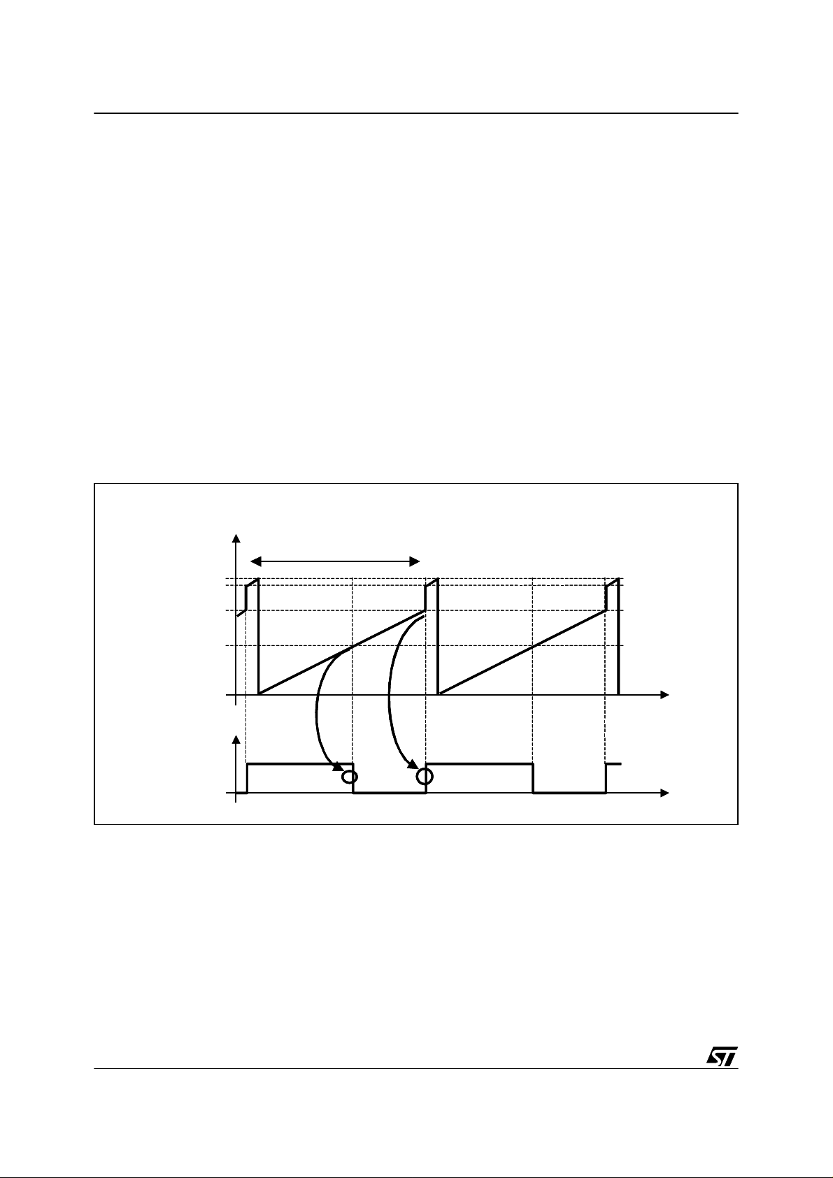
Figure 1 shows the normal behaviour of output compare 1 (OCMP1) pin when a PWM signal
is output with OLVL2=1 and OLVL1=0.
Figure 1. PWM output when O LVL2=1 and OLVL1=0
FREE RUNNING
FREE RUNNING
COUNTER VALUE
COUNTER VALUE
Ttimer × 65535
Ttimer × 65535
OLVL1=0
OLVL1=0
OLVL2= 1
OLVL2= 1
time
time
time
time
FFFFh
FFFFh
FFFCh
FFFCh
OC2R
OC2R
OC1R
OC1R
0000h
0000h
OCMP1
OCMP1
Ouput Compare pin
Ouput Compare pin
Timer output
Timer output
Tmax =
Tmax =
When the counter reaches the OC2R register value, the value of OLVL2 is applied on the
OCMP1 pin (=1 in this case). W hen the c ounter reaches the v alue of the O C1R register, the
value of OLVL1 is applied on the OCMP1 pin (= 0). The formulas needed to compute the
values to be put in OC2R and OC1R registers are in the 16- bit Timer chapter of the ST7 datasheets. As the 16-bit Timer is reset at FFFC, the formulas are:
OCiR=((t*Fcpu)/presc)-5 where:
t= period of the signal
2/9
2
Page 3
STARTING A PWM SIGNAL DIRECTLY AT HIGH LEVEL USING THE ST7 16-BIT TIMER
Fcpu= CPU frequency
presc= Timer 16 presc
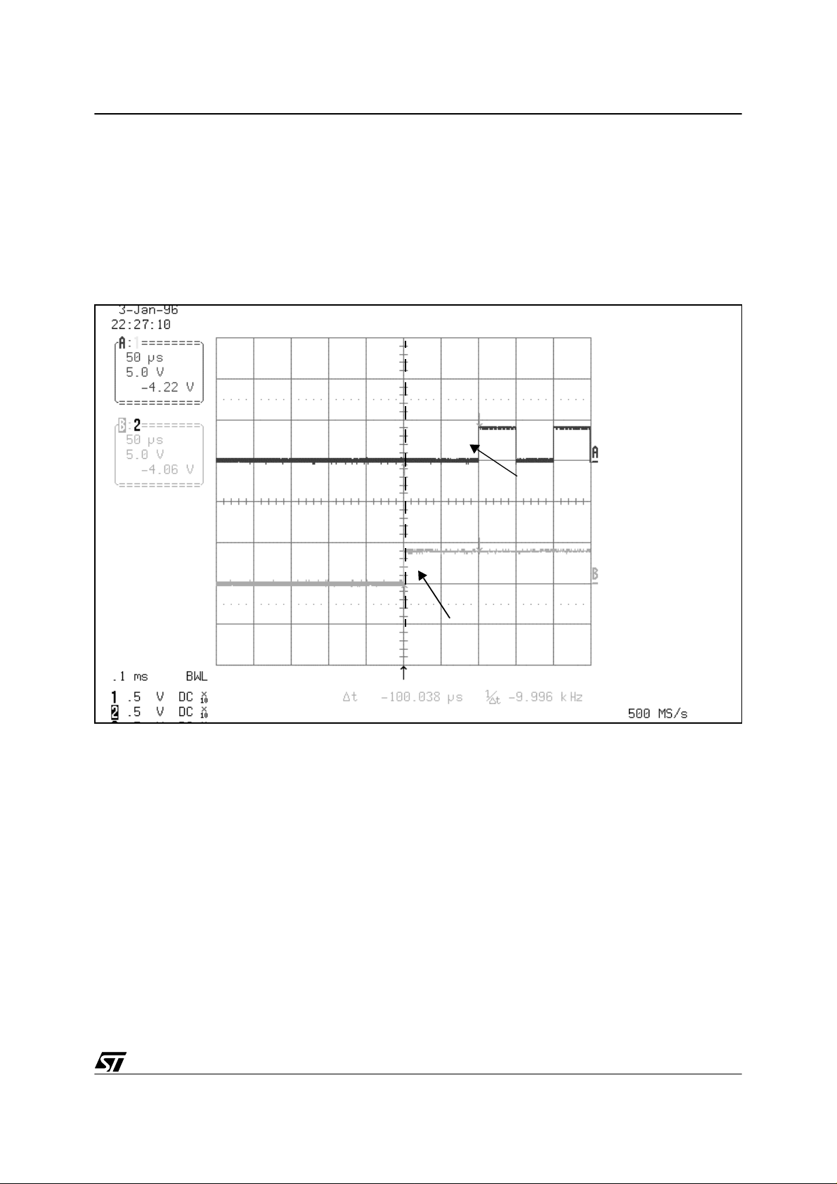
Figure 2 show s the wav ef orms we see on an osc illos cope if th e PWM s ignal is ini tialized a t
10KHz with a 50% duty c ycle (OLVL2=1 and OLVL1=0) and if a flag is set as soon as the
counter is started.
Figure 2. OCMP1 waveform with 50% Duty Cycle
PWM
OUTPUT
Timer 16 start
output enabled
flag
We can see from this figure that we have to wait until the counter reaches the OC2R r egister
value to get the first high state on the OCMP1 pin. So we have lost one PWM cycle before getting the first high level and in some applications, like energizing motor windings, this is not acceptable. After a motor demagnetization phase, if the windings are not energized immediately
when the PWM is started, the motor can stall. The purpose of the following sections is to explain how to get a high level on OCMP1 pin immediately.
To solve the problem, we have to handle two cases.
1. The PWM signal is high when the timer is between F FFC (its reset value) and the OC1R
register value. This means OLVL1=0 and OLVL2=1.
2. The PWM signal is high when the timer is between the OC1R register value and the OC2R
register value. This means OLVL1=1 and OLVL2=0.
3/9
Page 4

STARTING A PWM SIGNAL DIRECTLY AT HIGH LEVEL USING THE ST7 16-BIT TIMER
2 FIRST CASE: OLVL2=1 AND OLVL1=0
In this case, to force a high state on the OCMP1 pin when the timer is started:
– Initialize the timer in PWM mode and set the PWM frequency with a 0% duty cycle
– Reset the timer (at FFFC)
– Load the OC1R register with a value close to FFFC (FFFD for example) and configure
OLVL1=1 and OLVL2=0.
– Start the timer. It immediately reaches the value of the OC1R register and OCMP1 pin goes
into the state defined by the OLVL1 bit, which is high.
– Then, write the correct duty cycle value in the OC1R register and the correct state in the
OLVL2 and OLVL1 bits (OLVL2=1 and OL VL1=0).
The following code gives an example of how to restart (or start) the 16-bit timer this way. This
is for Timer A already ini tiali zed in PWM mode at 10KHz with the 16- bit timer clocked at 1MHz
(TACR2=10011000, TAOC2HR=$00 and TAOC2LR=$5F for 10KHz at 1MHz clock.
This is how to calculate the values to be put in the registers:
– OC2R represents the signal period. The frequency is 10KHz, so the period is t=100µs. f
CPU
is 8MHz and the Timer prescaler is 8 because the Timer is at 1MHz.
OC2R=((t*Fcpu)/presc)-5=((100.10-6*8.10+6)/8)-5=95 (005F in hexadecimal).
– OC1R represents the pulse length, the duty cycle is 50% so the pulse length is
100µs*50%=50µs. So the value to be put in OC1R is:
OC1R=((50.10-6*8.10+6)/8)-5=45 (002D in hexadecimal).
Note: This method can be applied when the counter is first started as the starting value is
0000.
Initialization: In this example the duty cycle is first set to 0% with OLVL1=0 and OLVL2=0
ld A,#%00000000; set OLVL1=0 and OLVL2=0
ld TACR1,A
ld A,#%10011000; clock in/8=1MHz with 16 MHz quartz
ld TACR2,A
ld A,#$00
ld TAOC2HR,A ;10KHz frequency for the PWM signal (see formulas)
ld A,#$5F
ld TAOC2LR,A
Synchronization
ld A,#%00000001;Set OLVL1=1 and OLVL2=0
ld TACR1,A ;load corresponding control register 1
ld A,#$FF
ld TAOC1HR,A ;fix compare 1 to FFFD to force PWM high as soon as possible
ld A,#$FD
4/9
Page 5

STARTING A PWM SIGNAL DIRECTLY AT HIGH LEVEL USING THE ST7 16-BIT TIMER
ld TAOC1LR,A
clr TACLR ;reset timer B to FFFC
bset PADR,#2 ;set flag synchronisation of timer B
.wait_TA_C2
ld A,TACHR
jrne wait_TA_C2;wait timer A=0000 to restore duty cycle
ld A,#%00000100
ld TACR1,A ;set OLVL1=0 and OLVL2=1
ld A,#$00
ld TAOC1HR,A
ld A,#$2D ;restore duty cycle to 50%
ld TAOC1LR,A
bres PADR,#2 ;reset synchronisation flag
Figure 3 shows the waveforms seen on an oscilloscope for OCMP1 pin and the sy nchronization flag using the above software example when the 16-bit timer is started or restarted.
Figure 3. OCMP1 and synchronization flag : OLVL2=1 and OLVL1=0
PWM
OUTPUT
Timer 16 start
output enabled
flag
We can see in Figure 3 that the OCMP1 pin outputs a high state directly after starting the
PWM signal. This avoids losing a PWM cycle in applic ations where an i mmediate high state is
required.
5/9
Page 6

STARTING A PWM SIGNAL DIRECTLY AT HIGH LEVEL USING THE ST7 16-BIT TIMER
3 SECOND CASE: AND OLVL1=1 AND OLVL2=0
Figure 4. PWM output when OLVL2=0 OLVL1=1
FREE RUNNING
FREE RUNNING
COUNTER VALUE
COUNTER VALUE
Ttimer × 65535
Ttimer × 65535
OLVL1=1
OLVL1=1
OLVL2= 0
OLVL2= 0
time
time
time
time
FFFFh
FFFFh
FFFCh
FFFCh
OC2R
OC2R
OC1R
OC1R
0000h
0000h
OCMP1
OCMP1
Ouput Compare pin
Ouput Compare pin
Timer output
Timer output
Tmax =
Tmax =
In this case, the timer A is also initialized at 10KH z with a 1MHz timer clock.
We can see that when OLVL2=0 and OLVL1=1, to set the duty cycle value, the OC1R register
has to be loaded with the complemen tary value= compare 2-(the normal value of Compare 1
in the Case 1 example). So for example, with a 10KHz PWM signal with a 1MHz timer clock,
we have OC2R register =005F (see formulas) and so for 20% duty cycle, the normal value of
the OC1R register is:
OC1R=((20.10-6*8.10+6)/8))-5=15 (000F in hexadecimal)
The complementary value is then OC1R=005F-000F=0050 in hexadecimal.
For the initialization phase, we need to set a 0% duty cycle and in this case, instead of config-
uring OLVL2=OLVL1=0 we can simp ly put a higher value in the OC1R register than in the
OC2R register. This following code example is for a 20% duty cycle signal.
Initialization: Set up 10KHz PWM signal with OLVL2=0 and OLVL1=1 and 0% duty cycle
ld A,#%00000001; set OLVL1=1 and OLVL2=0
ld TACR1,A
ld A,#%10011000;Clock in/8: 1MHz with 16 MHz quartz
ld TACR2,A
ld A,#$00
ld A,TAOC2HR ;compare 2 of timer A set 005F=100-5=95
ld A,#$5F
ld TAOC2LR,A ;frequency set to 10KHz
6/9
Page 7

STARTING A PWM SIGNAL DIRECTLY AT HIGH LEVEL USING THE ST7 16-BIT TIMER
ld A,#$00
ld TAOC1HR,A
ld A,#$60
ld TAOC1LR,A ; set 0% duty cycle by compare 1 value > compare 2 value
After this initial ization , the PW M sy nchro nizat ion at st art is don e by pu ttin g a value into the
compare register that is just higher than the timer restart value.
Synchronization:
ld X,#$FF ;set compare 1 to FFFD just after the timer reset value FFFC
ld TAOC1HR,X ;to force the output PWM high just after restart
ld A,#$FD
ld TAOC1LR,A
add A,#$0F ;ld compare 2 with compare 1+20% duty (000F)
ld Y,A
ld A,X
adc A,#$00
ld TAOC2HR,A
ld TAOC2LR,Y
clr TACLR ;reset timer A to FFFC
bset PADR,#2 ;set synchronization flag of timer A
.wait_TA_C1
ld A,TACHR
jrne wait_TA_C1;wait timer A counter=0000 to restore compare 1
ld A,#$00
ld TAOC1HR,A
ld A,#$50
ld TAOC1LR,A ;restore compare 1 to 20% (compare 2*(1-20%))
.wait_TA_C2
btjf TACHR,#7,wait_TA_C2;wait for reset of timer A before restoring com-
pare 2 value
ld A,#$00
ld TAOC2HR,A
ld A,#$5F ;restore compare 2 to 10KHz=100-5=95 (see formulas)
ld TAOC2LR,A
bres PADR,#2 ;reset synchronization flag of timer B
7/9
Page 8

STARTING A PWM SIGNAL DIRECTLY AT HIGH LEVEL USING THE ST7 16-BIT TIMER
Figure 5. OCMP1 and flag : timer restart between compare 1 and compare 2
PWM
OUTPUT
Timer 16 start
output enabled
flag
We can see on this figure that the OCMP1 pin outputs a high state immediately after starting
the PWM signal with the 16 bit timer. This will avoid wasting PWM cycle for applications where
an immediate high state is needed.
8/9
Page 9

STARTING A PWM SIGNAL DIRECTLY AT HIGH LEVEL USING THE ST7 16-BIT TIMER
“THE PRESENT NOTE WHICH IS FOR GUIDANCE ONLY AIMS AT PROVIDING CUSTOMERS WITH INFORMATION
REGARDING THE IR PRO DUCT S IN OR DER FO R THEM TO SAV E TIME . AS A RES ULT, STMIC ROEL ECTR ONI CS
SHALL NOT BE HELD LIABLE FOR ANY DIRECT, INDIRECT OR CONSEQUENTIAL DAMAGES WITH RESPECT TO
ANY CL AIM S AR IS IN G FR OM T HE CO N TENT OF S UC H A NO TE A ND /O R T HE U SE M AD E BY C US TO ME RS O F
THE INFORMATION CONTAINED HEREIN IN CONNEXION WITH THEIR PRODUCTS.”
Information furnished is believed to be accurate and reliable. However, STMicroelectronics assumes no responsibility for the consequences
of use of such information nor for any infringement of patents or other rights of third parties which may result from its use. No license is granted
by implic ation or otherwise under any patent or patent ri ghts of STM i croelectr oni cs. Spec i fications mentioned i n this publication are subje ct
to change without notice. This publication supersedes and replaces all information previously supplied. STMicroelectronics products are not
authorized for use as cri tical comp onents in life support dev i ces or systems wi thout the express written approv al of STMicroel ectronics.
The ST logo is a registered trademark of STMicroelectronics
2002 STMicroelectronics - All Rights Reserved.
STMicroelectronics Group of Compan i es
http://www.s t. com
Purchase of I
2
C Components by STMicroelectronics conveys a license under the Philips I2C Patent. Rights to use the se components in an
2
I
C system i s granted pro vi ded that the sy stem conforms to the I2C Standard Specification as defined by Philips.
Australi a - B razil - Canada - China - Finl and - France - Germany - Hong Kong - Ind ia - Israel - Italy - Japan
Malaysi a - M al ta - Morocco - Singapore - Spain - Sw eden - Switz erland - United Kingdom - U.S.A.
9/9
 Loading...