

Page 1

AN1496
APPLICATION NOTE
Flash Programming / Reprogramming ST10F269 / ST10F280
By André ROGER
INTRODUCTION
This application not e provides with software guidelines and examples for programming ST10F269 and
ST10F280. More generally, this application note is applicable for any ST10 variant with 0.35µm
technology embedded Flash memory.
The first chapter gives an overview the ST10F269/ F2 80 em bedded Flash key features. It also shows the
differences between ST10F269/ST10F280 and ST10F 168.
The second chapter de scribes h ow to develop software for ST10’s embedded Flash t hrough guidelines,
examples and tips.
The last chapter is dedicat ed to embedded application aspects. More specifically, it gi ves advises for
Flash field reprogramming.
This application note do es not replace ST10 p roduct datashe ets. It refers to them and it is necessary to
have a copy the specific ST10 variant targetted by the user to follow some of the explanations.
1/16February 2002
Page 2

AN1496 - APPLICAT ION NOTE
TABLE OF CONTENTS PAGE
1 INTRODUCTION TO ST10 0.35MM EMBEDDED FLASH ......................................... 3
1.1 DIFFERENCES WITH ST10F 1 68..... ............ ............ ............ ....................... ............ ... 3
1.1.1 Single Supply.................................................................................... ................... ........ 3
1.1.2 New Erase/Program Controller.................................................................................... 3
1.1.3 Improved Granularity of Block Sizes ........................................................................... 3
1.2 COMPARISON WITH STAND-ALONE FLASH MEMORIES...................................... 3
1.2.1 Similar But Different Erase/Program Commands........................................................ 3
1.2.2 Description of the Commands to the Flash Controller................................................. 3
1.2.3 Same Flash Status Register ........................................................................................ 5
1.2.4 Bo o t Blocks Architecture .......... ....................... ............ ............ ............ ............ ............ 6
1.2.5 Pr o tection ........... ........................ ............ ............ ............ ........... ........................ .......... 6
2 WRITING CODE FOR THE FLASH OF ST10 WITH 0.35MM EMBEDDED FLASH.. 7
2.1 ST10 PROGRAMMING CONSTRAINTS .................................................................... 7
2.2 POLLING THE FLASH ERASE PROGRAM CONTROLLER..................................... 7
2.2.1 Ready/Busy Signal ...................................................................................................... 7
2.2.2 Flash Status Register .................................................................................................. 7
2.3 FLASH MEMORY MAPPING IN ST10 SPACE........................................................... 7
2.4 PROGRAMMING COMMAND.................. ............ ........................ ............ ........... ........ 8
2.5 ERASING COMMAND ................................................................................................ 9
2.6 FLASH PROTECTION COMMANDS.......................................................................... 10
2.6.1 Block Protection..... ............ ....................... ............ ............ ............ ............ ................... 10
2.6.2 Code Protection........................................................................................................... 10
2.6.2.1 Using Code Protection with ST10................................................................................ 10
2.6.2.2 Code Protection and Bootstrap Loader . ...................................................................... 10
2.6.2.3 Code Protection and Block0 Protection....................................................................... 11
2.7 OTHER FLASH COMMANDS..................................................................................... 12
2.8 TIPS TO REDUCE FLASH PROGRAM AND ERASE TIMES .................................... 12
2.8.1 Reducing the Programming Time................................................................................ 12
2.8.2 Reducing Erase Times ........................................................................................ ........ 12
3 EMBEDDED APPLICATION ASPECTS..................................................................... 13
3.1 READING THE FLASH WHILE ERASING OR PROGRAMMING .............................. 13
3.1.1 Minimum Software to be Copied into the On-chip RAM.............................................. 13
3.1.2 Maximizing Programming Performance at System Level............................................ 13
3.1.3 Suspend and Resume Commands.............................................................................. 13
3.2 FIELD REPROGRAMMING WITH ST10F269 ............................................................ 14
3.2.1 Reset ........................................................................................................................... 14
3.2.2 List of Events and Suggested Handling Methods........................................................ 14
3.2.2.1 Supply out of ST Specification. .................................................................................... 14
3.2.2.2 ST10 PLL Unlock......................................................................................................... 14
3.2.3 Generic Aspects of Flash Field Reprogramming......................................................... 14
3.2.3.1 Completion of the Reprogramming Process................................................................ 15
3.2.3.2 Events That May Interrupt the Reprogramming Process ............................................ 15
4 QUICK SUMMARY ..................................................................................................... 16
5 CONCLUSION ............................................................................................................ 16
6 APPLICATION NOTE VERSION INFORMATION...................................................... 16
6.1 REVISION OF 26TH OF FEBRUARY 2002................................................................ 16
2/16
Page 3

AN1496 - APPLICAT ION NOTE
1 - INTRODUCTION TO ST10 0.35µm EMB E DDED FL A SH
This chapter is describing the improvements made from the ST10F168 and the differences with
stand-alone Flash memories.
1.1 - Differences with ST10F168
1.1.1 - Single Supply
ST10 variants with 0.35µm embedded Flash do not require specific programming supply. On-chip charge
pumps will provide with the necessary programming supply from the external single 5 volt supply.
1.1.2 - New Erase/Program Controller
The 0.35µm Erase/Program Controller has been changed to be closer to the one of stand-alone Flas h
memories : erasing and programming of Flash memory cells is no more done by the ST10. This allows :
Savings on system stack :
–
ing and programming,
Improved efficiency during programming :
–
the time where the Erase/Program Controller is dealing with the Flash,
Improved clock scheme :
–
to specify it the CPU clock. This also simplifies the hand ling of special events (like PLL unlock) during
erasing/programming.
there is no more need to allocate space on the ST10 system stack f or eras-
ST10 CPU can be used to handle communication during
the Flash erase/program controller has its own clock; there is no more need
1.1.3 - Improved Granularity of Block Sizes
ST10 0.35µm embedded Flash has improved block granulaty (smaller blocks) and also features boot
block organisation :
– Block size is 64 Kbyte for standard blocks,
– Small blocks for the 4 boot blocks (16 Kbyte, then 8 Kbyte, 8 Kbyte, 32 Kbyte).
1.2 - Comparison with Stand-alone Flash Memories
1.2.1 - Similar But Different Erase/Program Commands
The Erase/program Controller of ST10F269/F280 is derived from the Common Flash memory Interface :
– To keep the same level of proven safety, the special sequence of commands of stand alone Flash mem-
ories has been kept,
– To differentiate from ex ternal Flash memories, the value of the commands (address and data) have
been slighlty modified.
This allows to re-use existing software written for stand-alone Flash memories with few modifications. The
following chapters describe them.
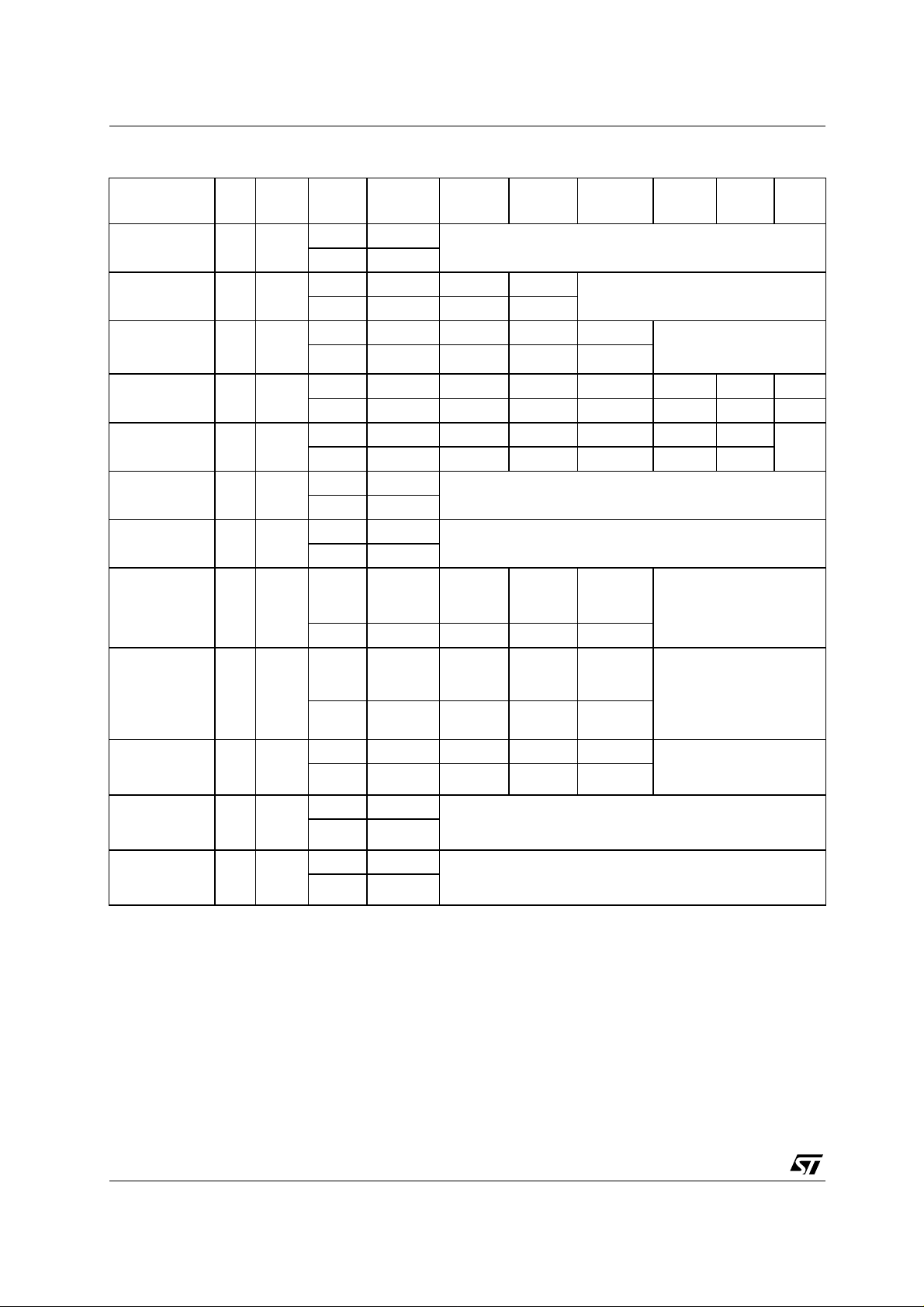
1.2.2 - Description of the Commands to the Flash Controller
The following table is describing the possible commands with ST10F269/F280 Erase/Program Controller.
Commands to the Flash are defined by a sequence of ST10 write cycles with specific addresses and data
within the Flash memor y range. The length of the seq uence varies from 1 cycle (ex : Read/Reset) to 6
cycles (chip erase).
Block erase command can be extended by 1 cycle per additional block to erase. This translates in a
maximum of 12 cycles for ST10F2 69 and of 16 cycles for ST10F280.
3/16
Page 4
AN1496 - APPLICAT ION NOTE
Table 1 :
Commands for ST10 with 0.35µm embedded Flash
Instruction Mne Cycle
Read/Reset RD 1+
Read/Reset RD 3+
Program Word PW 4
Block Erase BE 6
Chip Erase CE 6
Erase Suspend ES 1
Erase Resume ER 1
Set Block/Code
Protection
SP 4
Read
Protection
Status
RP 4
Block
Temporary
BTU 4
Unprotection
Code
Temporary
CTU 1
Unprotection
Code
Temporary
CTP 1
Protection
st
1
Cycle
Addr.
1
2
X
Data xxF0h
1
Addr.
x1554h x2AA8h xxxxxh
Data xxA8h xx54h xxF0h
1
Addr.
x1554h x2AA8h x1554h WA
Data xxA8h xx54h xxA0h WD
1
Addr.
x1554h x2AA8h x1554h x1554h x2AA8h BA BA’
nd
2
Cycle
3rd Cycle 4th Cycle
5th
Cycle
6th
Cycle
Read Memory Array until a new write cycle is initiated
Read Memory Array until a new write
cycle is initiated
3
Read Data Polling or
Toggle Bit until Program
4
completes.
7th
Cycle
Data xxA8h xx54h xx80h xxA8h xx54h xx30h xx30h
1
Addr.
Data xxA8h xx54h xx80h xxA8h xx54h xx10h
Addr.
Data xxB0h
Addr.
Data xx30h
Addr.
Data xxA8h xx54h xxC0h WPR
x1554h x2AA8h x1554h x1554h x2AA8h x1554h
1
2
X
Read until Toggle stops, then read or program all data needed
from block(s) not being erased then Resume Erase.
1
2
X
Read Data Polling or Toggle bit until Erase completes or Erase
is supended another time.
1
x2A54h x15A8h x2A54h Any odd
word
address
9
7
Note
Addr.1x2A54h x15A8h x2A54h Any odd
word
address
Data xxA8h xx54h xx90h Read
Read Protection Register
9
until a new write cycle is
initiated.
PR
Addr.
1
x2A54h x15A8h x2A54h X
2
Data xxA8h xx54h xxC1h xxF0h
1
Addr.
Data FFFFh
1
Addr.
Data FFFBh
MEM
MEM
8
Write cycles must be executed from Flash.
8
Write cycles must be executed from Flash.
5
6
Notes 1. Address bi t A14, A15 and above are don’t care for coded address inputs.
2. X = Don’t Care.
3. WA = Write Address: address of memor y location t o be programmed.
4. WD = Write Data: 16-bi t data to be programmed
5. Optional, add i tional blocks addresses must be entered within a time-out delay (96 µs) after l ast wr i te entr y, timeout st at us can be
verified through FSB.3 value. When full command is entered, read Data Polling or Toggle bit until Erase is completed or suspend ed.
6. Read Data Polling or Toggle bit until Erase completes.
7. WPR = W rite protection r egister. To pr ot ect code, bi t 15 of WPR must be ‘0’. To protect block N (N=0,1,. .. ), bit N o f WPR mu st be
‘0’. Bit that are already at ‘0’ in protection register must also be ‘0’ in WPR, else a writing error will occurs (it is not possible to write a
‘1’ in a bit already programmed at ‘0’).
8. MEM = any address inside the Flash memory spa ce. Absolut e addressing mo de must be used (MOV MEM, Rn), and inst ruction
must be executed from F l ash memory space.
9. Odd word address = 4n-2 w here n = 0, 1, 2, 3..., ex. 00 02h, 0006h. ..
4/16
Page 5

AN1496 - APPLICAT ION NOTE
1.2.3 - Same Flash Status Register
The Flash Status register is used to flag the status of the Flash memory and the result of an operation.
To maximise the re-use of Flash programming software, the Flash Status register of stand-alone Flash
memories has been kept.
This register can be accessed by Read cycles during the program-Erase Controller operations. The
Erase/Program operation can be controlled by data polling on bi t FSB7 of Status Re gister, detection of
Toggle on FSB6 and FSB2, or Error on FSB5 and Erase Timeout on FSB3 bits. Any read attempt in Flash
during Erase/Program. operation will automatically output these five bits. The E.P.C. sets bits FSB2,
FSB3, FSB5, FSB6 and FSB7. Other bits are reserved for future use and should be masked.
Flash Status (see note for address)
1514131211109876543210
Bit Function
FSB.7
FSB.6
FSB.5
FSB.3
FSB.2
Flash Status Bit 7: Data Polling Bit
Programming Op eration: this bit outputs the complement of the bit 7 of the word being programme d, and
after completion, will output the bit 7 of the word programmed.
Erasing Operation: outputs a ‘0’ during erasing, and ‘1’ after erasing completion.
If the Block selected for erasure is (ar e) pro tected, FSB.7 wi ll be se t to ‘0’ for about 100 µs, and th en ret ur n
to the previous addressed memory data value.
FSB.7 will also flag the Erase Suspend Mode by switching from ‘0’ to ‘1’ at the start of the Erase Suspend.
During Program o peration in Erase Suspend Mo de, FSB.7 will have the same behaviou r as in nor mal Pro-
gram execution outside the Suspend mode.
Flash Status Bit 6: Toggle Bit
Programming or Erasing Operations: successive read operations of Flash Status register will deliver complementar y values. FSB.6 will toggle each time the Flash Status register is read. The Program operation is
completed when two successive reads yield the same value. Th e next read will output the bit last programmed, or a ‘1’ after Erase operation
FSB.6 will be set to‘1 ’ if a re ad op eration is attempted on a n Erase S uspe nded block. In additio n, an Erase
Suspend/Resume command will cause FSB.6 to toggle.
Flash Status Bit 5: Error Bit
This bit is set to ‘1’ when there is a failure of Program, Block or Chip Erase operations.This bit will also be set
if a user tries to program a bit to ‘1’ to a Flash location that is currently programmed with ‘0’.
The error bit resets after Read/Reset instruction.
In case of success, the Error bit will be set to ‘0’ during Program or Erase and then will output the bit last pro-
grammed or a ‘1’ after erasing
Flash Status Bit 3: Erase Time-out Bit
This bit is set to ‘1’ by the P/E.C. when th e last Block Erase c ommand ha s been ente red to the C ommand
Interface and it is awaiting the Erase start. Wh en the time-out per iod is finished, aft er 96 µs, FSB.3 returns
back to ‘1’.
Flash Status Bit 2: Toggle Bit
This toggle bit, tog ether with FSB.6, can be used to dete rmine the chip status during the Erase Mode or
Erase Suspend Mode. It can be used also to identifiey the block being Erased Suspended. A Read operation
will cause FSB.2 to Toggle during the Erase Mode. If the Flash is in Erase Suspend Mode, a Read operation
from the Erase suspended block or a Program operation into the Erase suspended block will cause FSB.2 to
toggle.
When the Flash is in Pro gram Mode dur ing Eras e Susp end, FSB.2 will be read a s ‘1’ if ad dress used is the
address of the word being programmed.
After Erase completion with an Error status, FSB.2 will toggle when reading the faulty sector.
FSB.7 FSB.6 FSB.5 FSB.3 FSB.2
RRR RR
Note :
The address of the Flash Status Register is the address o f the word being programmed when
Programming operation is in progress, or an address within the block being erased when Erasing
operation is in progress.
5/16
Page 6

AN1496 - APPLICAT ION NOTE
1.2.4 - Boot Blocks Architecture
ST10 with 0.35µm embedded Flash has the same boot blocks as the M29F400 stand-alone Flash : 4 boot
blocks (16 Kbyte, then 8 Kbyte, 8 Kbyte and 32 Kbyte).
1.2.5 - Protection
Compared to stand-alone Flash memories, ST10 with embedded Flash provides with 2 different
protections :
– Block protection, as already implemented on ST stand-alone Flash memories, protects each block
against inadvertent erasing,
– Code protection, is a set of new com mands to prot ect the proprietary code written in the Flash : code
protection disables data operands accesses and program branches from any location outside the embedded Flash.
The different protections are c ontrolled through t he Fla sh Protection register. It is identical of the on e of
stand-alone Flash memories except for the code protection.
The Flash Protection register is a non-volatile register that contains the protection status. This register
can be read by using the Read Protection Status (RPS) command, and programmed by using the
dedicated Set Protection command .
Flash Protection Register (PR)
1514131211109876543210
CP BP10 BP9 BP8 BP7 BP6 BP5 BP4 BP3.3 BP2.2 BP1 BP0
Bit Function
BPx
Note :
Block x Protection Bit (x = 0...10)
‘0’: the B lock Protectio n is en abled for block x. Pro gramming or erasing t he block is n ot possible, unless a
Block Temporary Unprotection command is issued.
1’: the Block Protection is disabled for block x.
Bit is ‘1’ by default, and ca n be p rogrammed permanently to ‘0’ us ing th e Set Prote ction comm and but then
can not be set to ‘1’ again. It is therefore possible to temporally disable the Blo ck Protection using the Blo ck
Temporary Unprotection instruction.
Code Protection Bit
CP
‘0’: the Flas h Code Protection is enabled.Read acce sses to the Flash for execution not performed in the
Flash itself are not allowed, the returned value will be 009Bh, whatever the content of the Flash is.
1’: the Fla sh Code Protect ion is disabled: read accesses to t he Flash from exter nal or interna l RAM are
allowed
Bit is ‘1’ by default, and ca n be p rogrammed permanently to ‘0’ us ing th e Set Prote ction comm and but then
can not be set to ‘1’ again . It is therefore possible to tem porally di sable the Cod e Prote ction us ing the Co de
Temporary Unprotection instruction.
The organisation of the Flash control register depends on the organisation of each device. Please,
refer to the targetted product datasheet (ex : ST10F269 : BP10, BP9, BP8, BP7 are not implemented).
6/16
Page 7

AN1496 - APPLICAT ION NOTE
2 - WRITING CODE FOR THE FLASH OF ST10 WITH 0.35µm EMBEDDED FLASH
2.1 - ST10 Programming Constraints
Programming Language:
Direct addressing is not allowed for command sequences. All addresses of command cycles shall be
defined only with
As the compiler may generate indirect addressing, the part of the software that generates the
to the Flash should be written in assembly.
commands can be in higher level lan guage (ex : C).
Indirect addressing :
For command instructions, address bit A 14, A15, A16 and A17 are don’t care, provided the generated
address falls within the Flash memory space.
This allows to simplify the use of DPP registers when generating com mands to the Flash : any DPP
already pointing to data in the Flash memory space can be used to write com man ds to the Flash.
Tip :
–
It is also possible to use the extended segment or extended page instructions for addressing the
Flash.
2.2 - Polling the Flash Erase Program Con troller
As soon as the Erase Program Controller (EPC) receives the last command of a command sequenc e, it
starts execution of the command. During command execution, the EPC status is indicat ed by 2 sources :
– The Flash Status Register,
– The Read/Bus t signal.
The Flash automatically resumes the read mode after the completion of the command.
Register-indirect
addressing mode.
commands
Still part of the software that is not generating the
2.2.1 - Ready/Busy Signal
The Ready/Busy (R
/B) signal is connected to the X PER2 interrupt node (XP2IC). Whe n R is high, the
Flash is busy with a Program or Erase operation and will not accept any additional program or erase
instruction. When R
/B is Low, the Flash is ready for any Read/Write or Erase operation. The R/B will also
be Low when the memory is put in Erase Suspend mode.
This signal can be polled by reading XP2IC register, or can be used to trigger an interrupt when the Flash
goes from Busy to Ready.
This feature may not be available for all ST10 variants in 0.35µm technology (ex : not available for
ST10F280). Please, check the product datasheet.
2.2.2 - Flash Status Register
The Flash Status register has been described in the previous chapter.
This method of polling ST10 embedded Flash is the one recommanded : the method will be implemented
on all ST10 variants in 0.35µm technology.
2.3 - Flash Memory Mapping in ST10 Space
As defined for all ST10 derivatives, the lower 32 Kbyte part of the embedded Flash memory can be
mapped into 2 different segments.
The Flash mapping is controlled by bit ROMS1 in register SYSCON.
Table 2 :
FLASH Memory Block Mapping
Block Addresses (Segment 0) Addresses (Segment 1) Size (bytes)
0
1
2
00’0000h to 00’3FFFh
00’4000h to 00’5FFFh
00’6000h to 00’7FFFh
01’0000h to 01’3FFFh
01’4000h to 01’5FFFh
01’6000h to 01’7FFFh
16 K
8 K
8 K
Note :
the memory m apping of the other block is independant of bit ROMS1.
7/16
Page 8

AN1496 - APPLICAT ION NOTE
2.4 - Programming Command
In the examples hereafter, the 16-bit registers R11 and R12 are used as auxilary registers for indirect
addressing.
The following example s use DPP0. We just to have to make sure that DPP0 points to the active Flash
area.
To be independant of the mapping of sector 0, we choose here segment2 for DPP (i.e. : DPP0 = 08h).
Example :
We assume that in the i nitialization phase the lowest 32 Kbyte of Flash memory (sec tor 0) have been
mapped to segment 1. The data to be written is loaded in register R13, the address to be programmed is
loaded in register R11/R12 (segment number in R11, segment offset in R12).
; sending of the programming command to the Flash
MOV R5, #01554h ;load auxilary register R5 with command address
MOV R6, #02AA8h ;load auxilary register R6 with command address
SXCT DPPO, #08h ;push data page pointer 0 and load it to point
MOV R7, #0A8h ;load register R7 with 1st CI enable command
MOV [R5], R7 ;command cycle 1
MOV R13, #054h ;load register R7 with 2nd CI enable command
MOV [R6], R7 ;command cycle 2
MOV R13, #0A0h ;load register R7 with Program Word command
MOV [R5], R7 ;command cycle 3
POP DPP0 ;restore DPP0: following addressing to the Flash
EXTS R11, #1 ;use EXTended addressing for next MOV instruction
MOV [R12], R13 ;command cycle 4: the E/P.C. starts execution of
Performing a Program Word command
;(used in command cycle 1)
;(used in command cycle 2)
;to segment 2
;will use EXTended instructions
;R11 contains the segment to be programmed
;R12 contai ns the s egme nt o ffse t addre ss to be pr ogr amm ed
;R13 contains the data to be programmed
;Programming Command
; Data_Polling after word programming :
data_polling :
EXTS R11, #1 ;use EXTended addressing for next MOV instruction
MOV R7, [R12] ;read Flash Status register (FSB) in R7
MOV R6, R7 ;save it in R6 register
;Check if FSB.7 = Data.7 (i.e. R7.7 = R13.7)
XOR R7, R13
JNB R7.7, Prog_OK
;Check if FSB.5 = 1 (Programming Error)
JNB R6.5, Data_Polling
;Programm ing Erro r: ve rif y is F lash pr ogra mme d dat a is OK
EXTS R11, #1 ;use EXTended addressing for next MOV instruction
MOV R7, [R12] ;read Flash Status register (FSB) in R7
;Check if FSB.7 = Data.7
XOR R7, R13
JNB R7.7, Prog_OK
;Programming failed: Flash remains in Write Operation.
;To go back to normal Read operations, a Read/Reset
;command must be performed
8/16
Page 9

AN1496 - APPLICAT ION NOTE
Prog_Error:
MOV R7, #0F0h ;load register R7 with Read/Reset command
EXTS R11, #1 ;use EXTended addressing for next MOV instruction
MOV R12], R7 ;address is don’t care for Read/Reset command
... ;here place specific Error handling code
...
...
;When programming operation finshed succesfully, Flash
is set
;back automatically to normal Read Mode
Prog_OK:
....
....
2.5 - Erasing Command
Example :
We assume that in the i nitialization phase the lowest 32 Kbyte of Flash memory (sec tor 0) have been
mapped to segment 1. The registers R11/R12 contain an address related to the block to be erased
(segment number in R11, segment offset in R12, eg; R11 = 01h, R12= 4000h will erase the Block 1 - first
8 Kbyt e b lo c k ) .
Performing the Block Erase command
; sending of the erasing command to the Flash
MOV R5, #01554h ;load auxilary register R5 with command address
;(used in command cycle 1)
MOV R6, #02AA8h ;load auxilary register R6 with command address
;(used in command cycle 2)
SXCT DPPO, #08h ;push data page pointer 0 and load it to point
;to segment 2
MOV R7, #0A8h ;load register R7 with 1st CI enable command
MOV [R5], R7 ;command cycle 1
MOV R13, #054h ;load register R7 with 2nd CI enable command
MOV [R6], R7 ;command cycle 2
MOV R13, #080h ;load register R7 with Block Erase command
MOV [R5], R7 ;command cycle 3
MOV R7, #0A8h ;load register R7 with 1st CI enable command
MOV [R5], R7 ;command cycle 4
MOV R13, #054h ;load register R7 with 2nd CI enable command
MOV [R6], R7 ;command cycle 5
POP DPP0 ;restore DPP0: following addressing to the Flash
;will use EXTended instructions
;R11 contains the segment of the block to be erased
;R12 contains the segment offset address of the block
MOV R7, #030h ;load register R7 with erase confirm code
EXTS R11, #1 ;use EXTended addressing for next MOV instruction
MOV [R12], R7 ;command cycle 6: the E/P.C. starts execution of
;Erasing Command after 96us time-out delay
;additional block commands may be sent here before the
;96us time-out expires.
9/16
Page 10

AN1496 - APPLICAT ION NOTE
; erase polling during block erase
Erase_Polling:
EXTS R11, #1 ;use EXTended addressing for next MOV instruction
MOV R7, [R12] ;read Flash Status register (FSB) in R7
;Check if FSB.7 = ‘1’ (i.e. R7.7 = ‘1’)
JB R7.7, Erase_OK
;Check if FSB.5 = 1 (Erasing Error)
JNB R7.5, Erase_Polling
;Programming failed: Flash remains in Write Operation.
;To go back to normal Read operations, a Read/Reset
;command must be performed
Erase_Error:
MOV R7, #0F0h ;load register R7 with Read/Reset command
EXTS R11, #1 ;use EXTended addressing for next MOV instruction
MOV [R12], R7 ;address is don’t care for Read/Reset command
... ;here place specific Error handling code
...
...
;When erasing operation finshed succesfully, Flash is
;set back automatically to normal Read Mode
Erase_OK:
....
....
2.6 - Flash Protection Commands
2.6.1 - Block Protection
Block protection allows to protect Flash internal blocks against inadvertent erasing and/or programming.
For security reasons, once set, protection cannot be removed, even after erasing the Flash. It can only be
temporarily disabled using the "block temporary unprotection" command.
2.6.2 - Code Protection
Code protection allows to disable any read or jump to the ST10 embedded Flash from a nother mem ory
(like internal RAM, external memory).
For security reasons, once set, code protection is per m anent and c annot be c leared, even after erasing
the Flash. Code protection can only be temporary disabled using the "code temporar y unprotection"
command.
Code temporar y unprotection rema ins active until a code temporar y prot ection command is executed or
until reset (reset via the Flash Command Interface, hardware, software, watchdog)
2.6.2.1 - Using Code Protection with ST10
When code prot ection is set, and when code may be executed from another memor y before resuming
code from on-chip-Flash, the code protec tion should be disabled before calling the routine in the other
memory. If not, a Trap #00 illegal instruction will be generated when jumping back to the on-chip Flash.
2.6.2.2 - Code Protection and Bootstrap Loader
The code protection also applies in bootstrap mode : in ST10 boostrap loader mode, it is not possible to
read the Flash or to jump into any address within the embedded Flash.
10/16
Page 11

AN1496 - APPLICAT ION NOTE
2.6.2.3 - Code Protection and Block0 Protection
When code protection is set, it is still possible to erase and reprogram blocks that are not protected. As a
consequence, if block0 is not protected , it would still be possible to erase block0 and reprogram it with a
software to dump the remaining par t of the Flash.
If block0 is protected when code protection is set, it is not possible to dump the Flash content.
Example :
Performing the command Read protection
;***************************************************************************
*****
;Read_Block_Protection
;INPUT : NONE
;OUTPUT: R0 contain the status of each block (if bit x is set, block x is
protected)
;***************************************************************************
*****
Read_Block_Protection proc near
; R0 = segment of Flash
push R1 ; R1 = First addr to write
push R2 ; R2 = Second addr to write
push R3 ; R3 = Data
push R4 ; R3 = Data
push R5 ; R5 = pointer to data status
movR0, dpp2:Flash_Seg
mov R1, #Even_comm ; Retreive the even command addr
mov R2, #Odd_comm; Retreive the odd command addr
mov R3, #Val1
exts R0, #1
mov[R1],R3; First write
mov R3, #Val2
exts R0, #1
mov[R2],R3; second write
mov R3, #090h
exts R0, #1
mov[R1],R3; third write
MOV R2,#8; R2 contain the number of block that remain to read
MOV R3,#0; R3 will contain the status
MOV R4,#1; R4 Mask for status
MOV R1, R0
EXTS #MONITOR_SEG,#1
MOVR5, #flash_status
POP R5 ; R5 = pointer to data status
POP R4
POP R3
POP R2
POP R1
RET
Read_Block_Protection ENDP
11/16
Page 12

AN1496 - APPLICAT ION NOTE
2.7 - Other Flash Commands
Example :
We assume that in the i nitialization phase the lowest 32 Kbyte of Flash memory (sec tor 0) have been
mapped to segment 1.
According to the usual way of ST10 data addressing with data page pointers, address bits A15 and A14
of a 16-bit command wr ite address select the data pag e pointer (DPP) which contains the upper 10 bits
for building the 24-bit physical data address. Address bits A13...A 0 represent the addres s offset . As the
bits A14...A17 are don’t care when written a Flash command in the Command Interface (CI), we can
choose the most conveniant DPPx register for address handling.
The following examples are making usage of DPP0. We just have to make sure, that DPP0 points to
active Flash memory space.
To be independent of mapping of sector 0 we choos e for
handling, to point to segment 2.
For this reason we load DPP0 with value 08h (00 0000 1000b).
MOV R5, #01554h ;load auxilary register R5 with command address
MOV R6, #02AA8h ;load auxilary register R6 with command address
SCXT DPPO, #08h ;push data page pointer 0 and load it to point
MOV R7, #0A8h ;load register R7 with 1st CI enable command
MOV [R5], R7 ;command cycle 1
MOV R7, #054h ;load register R7 with 2cd CI enable command
MOV [R6], R7 ;command cycle 2
MOV R7, #0F0h ;load register R7 with Read/Reset command
MOV [R5], R7 ;command cycle 3. Address is don’t care
POP DPP0 ;restore DPP0 value
Performing the command Read/Reset
;(used in command cycle 1)
;(used in command cycle 2)
;to segment 2
all
DPPs which are u sed for Flash address
2.8 - Tips to Reduce Flash Program and Erase Times
2.8.1 - Reducing the Programming Time
When block protection is enabled, block temporar y unprotection com mands shall be sent before erasing
or programming command.
As block unprotection remains active till the next reset, this means it is not necessary to repeat this
command for each word to program.
2.8.2 - Reducing Erase Times
Reducing erase time is simple with ST10 0.35µm embedded Flash. Several charge pumps are provided
for each block, so erasing two blocks does not take twice as long as erasing one block (erasing 2 blocks
still takes longer than erasing one block however). To benefit from the parallel erase, it is important to
issue all the blocks you want with one Block Erase command. The Chip Erase command also erases the
blocks in parallel.
Erasing a Block of Data
Erase commands perform two operations : first, they individually program each word to 0000h , then t hey
use the tunnel ling t o set al l bi ts to "1" at the same time. Erasing time of a block can be reduc ed by m ore
than 50% if all word are already programmed to 0000h.
This specificity can be used in application where blocks of data are copied from 1 block to another and the
old block is marked as "dirty". Wri tting all data to 0000h of a "dirty" block will save time when erasing of
this block will be pe rfor med.
12/16
Page 13

AN1496 - APPLICAT ION NOTE
3 - EMBEDDED APPLICATION ASPECTS
This chapter advises for embedded applications whe re the ST10 embedded Flash m emory may be the
only non volatile memory available.
Reading the Flash while programming and field reprogramming are the 2 specific points raised by single
chip embedded applications.
3.1 - Reading the Flash While Erasing or Programming
During erasing or programm ing, the entire Flash is not visible to the CP U, what ever the Flash-block is
erased or programmed. As a consequence on ST10 software :
– During erasing and programming, it is not possible to have acc ess to the interrupt vector table and so
all interrupts shall be disabled.
– Before erasing an d programming, a sma ll software loo p shall be copied from the Flash to the on -chip
RAM to run the minimum code needed to wait for the end of erasing or programming .
– If code protection is activated, it should be temporary disabled before executing the code copied into the
on-chip RAM.
There are 2 ways to deal with this constraint : one is minimizing the requirements in RAM space used
during erasing/programming and another one is maximizing the programming spee d by duplicating all
needed software into the on-chip RAM.
3.1.1 - Minimum Software to be Copied into the On-chip RAM
The minimum software to be copied into the on-chip RAM is :
– Functions sending the erasing and or programming commands to the ST10 embedded Flash,
– Functions polling t he Flas h status register for completion of the command and f or error (s ee det ailled
specification).
Example of usage :
some data in the ST10 embedded Flash dur ing nor mal operation.
This method can be implemented when i t is necessary to program and/or erase
3.1.2 - Maximizing Programming Performance at System Level
When the minimum software is copied i nto the on-chip RAM, during erasing and/or programming, the
CPU cannot run any other software (like communication) during that time.
To maximize programming performance, user could handle the whole part or a part only of the
communication handler. This requires :
– That more software is copied into the on-chip RAM,
– The communication handler is not using interrupts,
– The software loop polling the Flash status register is modified to handle the Communicat ion process.
Example of usage :
This method can be implemented when it is necessary to erase and program
(re-program) the whole Flash of the ST10.
3.1.3 - Suspend and Resume Commands
As stand-alone Flash memori es, the 0.35µm embedded Flash controller features suspend and resume
commands; this allows to suspend at any time the erasing or the programming proces s and resume it
later on.
Once suspend command is completed, the ST10 can access to a needed software routine (i.e.
communication driver) which has not been relocated in the on-chip RAM.
Example of usage :
Note :
the time for which the Flash is not available is unchanged but this gives the possibility to suspend
the error handler of the communication driver.
the process to run specific routines during Flash erasing or programming (ex : communication protocol).
13/16
Page 14

AN1496 - APPLICAT ION NOTE
3.2 - Field Reprogramming with ST10F269
Reprogramming in the field part or the whole application, requires to be able to deal safely with all the
possible events that may occur in the field during the reprogramming of the Flash.
This analysis is application dependant and has to be carefully conducted by the user. This section
assumes that users have experien ce with all the generic aspects of field reprogramming and will focus
only on ST10 sp ecifi c events.
3.2.1 - Reset
Whatever the possible causes of reset (spurious reset , external hardware reset, reset du e t o power-shut
down), Reset is one of the events possible during field reprogramming.
As reset may occur during the erasing o f the on-chip F lash before it is re-programmed, ST10 should be
able to read a valid code from the Fl ash at the next start-up.
As a consequence,
– Block-0 (i.e. : starting at physical address : 00’0000h) shou ld never be eras ed during field reprogram -
ming.
– Block0 should contain all the routines to allow to res tart the reprogramming ro utines (if those routines
are in another block, this block also should never be erased).
Note :
This restriction on block0 does not apply if ST10 Bootstrap Loader mode is used for field
reprogramming. (see code protection paragraph if code protection is used).
Flash Bock Write Protection :
It is recommanded to use the Flash "Set block protection" feature to protect the block(s) which contains all
the needed software to restart the reprogramming routines. Any inadvertent chip erase command will not
affect those p rote c te d blocks.
3.2.2 - List of Events and Su ggested Handling Met h ods
3.2.2.1 - Supply out of ST Specification
Detection Method :
User should have specific hardware to detect whenever Vcc comes out of ST specification an d generate
a hardware reset as long this condition exist.
Suggested Handling Method :
Restart the whole reprogramming sequence at module level (i.e. : erasing + programing).
3.2.2.2 - ST10 PLL Unlock
As Flash programming/erasing timings are not defined by the ST10, PLL unlock has no effect on the
Flash erasing and programming. Usually, PLL unlock will stop communication because of change in bit/
baud rate.
Detection Method :
Not necessary (to be checked with application specific constraints).
Suggested Handling Method :
Restart the whole programming sequence (i.e. : at module level).
3.2.3 - Generic Aspects of Flash Field Reprogramming
This part is giving few advices for the field reprogramming . Those advices are n ot spec ific t o ST 10; t hey
are generic to any embedded ap plication that reprograms itself using a c ommunication media with a
programming station.
The main points to control during Flash reprogramming are :
– Completion of the reprogramming process itself,
– Events that may interrupt the reprogramming process.
14/16
Page 15

AN1496 - APPLICAT ION NOTE
3.2.3.1 - Completion of the Reprogramming Process
The programming process is com pleted when the last word to be programmed has been programmed
correctly (i.e. : status returned by the Flash is OK). If, for any reason, the programming process is
interrupted during the programming of the last word, the value written may be good at the next rest art, but
the retention time of this value may be limited.
For this reason, it is recommanded that users consider the reprogramming to be "OK" only after the
completion of the programm ing of the last word (ex : send an acknowledge to the programming st ation
after the last word has been sucessfully programmed).
Evidence of completion of programming process :
For traceability reasons, some users may want to record an evidence of the successfull completion of the
reprogramming process.
This can be done by programming a variable into the Fla sh after the last valid word to be programmed.
3.2.3.2 - Events That May Interrupt the Reprogramming Process
There may be other events that could interrupt the reprogramming process.
The handling of those events, at module level and at ST10 level, should be such that those events are
detected as soon as possible and that the ST10 will be able to restart the programming process.
On ST10 side, as ST1 0 bank0 i s never erased, it will be possible to res tar t the programm ing process (if
we assume that all banks that have the code needed for reprogramming are never erased).
Restarting Reprogramming :
When interrupted, it is recommanded to restart the reprogramming process from the beginning (i.e. :
erasing
and
programming).
15/16
Page 16

AN1496 - APPLICAT ION NOTE
4 - QUICK SUMM ARY
This table gives a quick summary on ST10 programming for 0.35µm embedded Flash :
Addressing :
Prog ramming la nguage :
assembly to ensure register indirect addressing is used,
Polling the Flash Erase/Program Controller :
increased software re-use for coming ST10 variants, check that reserved bits are masked by software.
Code run from RAM :
commands should be run from the on-chip RAM,
Interrupt disabled :
Code prot ection :
memory (external Flash, on-chip RAM during bootstrap mode). For better protection, check that bock0 is
erased protected.
5 - CONCLUSION
This application note has shown how easy it is to erase and program ST10F269 and ST10F280.
It shows that ST10 with 0.35µm single voltage embedded Flash memory are ideal for embedded
applications where perform ance, sec uri ty and reprogramma bilit y are needed.
6 - APPLICATION NOTE VERSION INFORMATION
register indirect addressing needed for the commands to the embedded Flash,
can be high level (ex : C) except for the writting of the commands : must be in
preferred solution is via the Flash status register. For
the commands for erasing, programming and polling the completion of the
no interrupt enabled during the execution of commands into the Flash,
once set, it is no more possible to dump the Flash content from code in another
6.1 - Revision of 26th of February 2002
This is the first revision of the AN1496.
Information furnished is bel ieved to be accurate and reliable. However, STMicroe lectronics assumes no responsibility for the
consequences of use of such information nor for any infringement of patents or other rights of third parties which may result from
its use. No li cense is granted by implication or otherwise unde r any patent or patent rights of STMicroelectronics. Specifications
mentioned in this publication ar e subject to change without notice. This publication supersedes and replaces all information
previously supplied. S TMicroelectronics products are not authorized for use as critica l components in life suppo rt devices or
systems without express written approval of STMicroelectronics.
The ST logo is a registered trademark of STMicroelectronics
© 2002 STMicroelectronics - All Rights Reserved
STMicroele ct ronics GROUP OF COM PANIES
Australia - Brazil - Canada - Ch i na - F i nl and - France - Germany - Hong Kong - Ind i a - I srael - Italy - Japan - Mala ysia - Malt a - Mor oc co
16/16
Singapor e - S pai n - Sweden - Swi tzerland - United King dom - United States
http://www.st.com
 Loading...