

Page 1
AN1491
APPLICATION NOTE
IGBT BASICS
M. Aleo (mario.aleo@st.com)
1. INTRODUCTION.
IGBTs (Insulated Gate Bipolar Transistors) combine the simplicity of drive and the excellent fast
switchin g capabilit y of the MO SFET str ucture with the ability t o handle h igh curren t values t ypical of a
bipolar device. IGBTs also offer good behavior in terms of voltage drop. IGBT technology, developed in
the early 1980s, has quickly gaine d market share for app lications exceeding 400V and that work up to
130kHz. This paper includes a brief description of the structure and the physics of the device, followed by
an analysis of the principal static and dynamic characteristics. Further details about the behavior in
operation will also be analyzed and discussed in order to give a complete overview of the main
parameters, features, and static and dynamic behaviors of this power component.
2. IGBT STRUCTURE AND OPERATION.
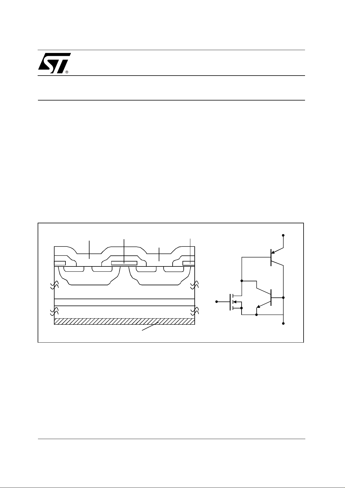
Figure 1: IGBT Structure And Equivalent Schematic
ALUMINUM
N+
NN+
P+
IGBTs are a natural evolution of the vertical Power MOSFETs for high current, high voltage applications
and fast end-equipment. This device eliminates the main disadvan tage of current high voltage power
MOSFETs characterized b y an high value of R
path necessary to obtain a high breakdown voltage BV
levels are considerably less in IGBT technology even when compared with the latest generation of Power
MOSFET devices that have been greatly improved in terms of R
N+ N+
P+
GATE
EMITTER
SUBSTRATE
COLLECTOR
POLYSILICON
N+
P+
caused by the high resistivity of the source-drain
DS(on)
DSS
J3
J2
J1
. The power conduction losses at high current
G
. The lower voltage drop,
DS(on)
C
E
December 2001
1/16
Page 2
AN1491 - APPLICATION NOTE
translated into a low V
standard bipolar device simpl ifying the IGBTs driver schematic as well. The vertical section depi cted in
figure 1 together with the equivalent circuit shows IGBTs basic structure.
3. TURN-ON.
The structure of the silicon die is evidently similar to that of a Power MOSFET with the fundamental
difference of the addition o f a P+ substrate a nd an N+ buffer layer (absent in NPT-non-punch-throughIGBT technology). This is represented in the equivalent schematic (figure 1), with a MOSFET driving two
bipolar devices. The presence of the substrate cre ates a junction J1 between t he P+ and th e N zone of
the body.
When the positive gate bias allows the inversion of the P base region under the gate, an N channel is
created, with a flow of electrons, generating a current in the exact same way as a Power MOSFET. If the
voltage caused by this flux is in the range of 0.7V, then J1 is forward biased and some holes are injected
in the N- region, modulating the resistance between anode and cathode, in this way decreasing the
overall power conduction losses and a second flow of charges starts.
The final result is the contemporary presence of two different typologies of current inside the
semiconductor’s layers:
- an electron flux (MOSFET current);
- a hole current (bipolar).
, together with the device’s structure allow a higher current density than a
CE(sat)
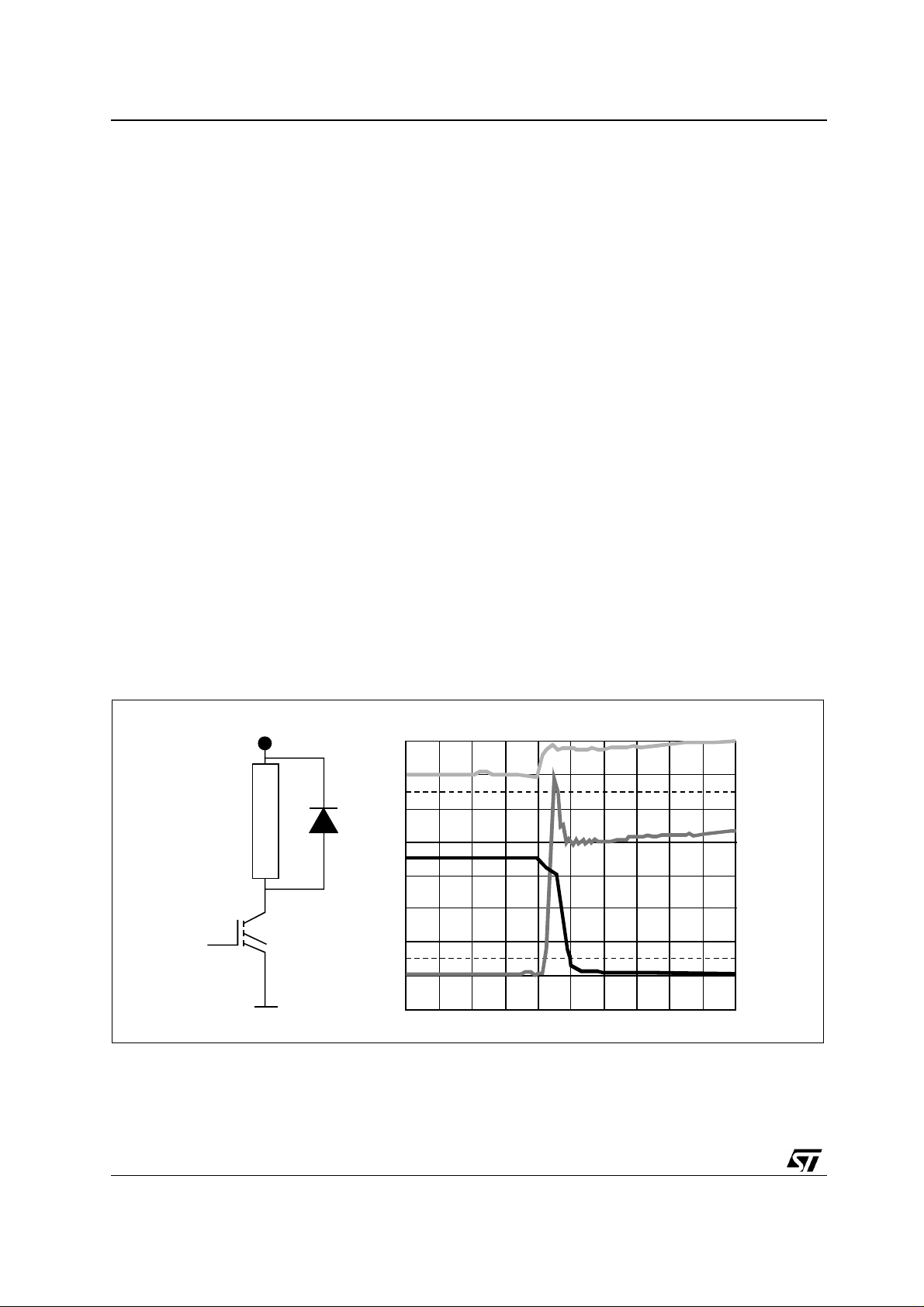
The typical waveforms with an inductive load are reported in figure 2.
Figure 2: Typical Waveforms During Turn-On
V
CC
V
ge
L
O
A
V
CE
D
I
C
gnd
2/16
Page 3
AN1491 - APPLICATION NOTE
4. TURN-OFF.
When a negative bias is applied to the gate or the gate voltage falls below the threshold value, the
channel is inhibited and no holes are i njected in the N- region . In any case even if the MO SFET current
decreases rapidly in t he switching off phase, the collector current gradual ly reduces because t here are
minority car riers still pre sent in the N laye r, immedia tely aft er th e start of c om mutati on. Th e d ecre ase i n
value of this residual current (tail) is strictly dependent on the de nsity of these charges in turn-off that is
linked to several factors as the amount of dopant, dopant typology, layers’ thickness and temperature.
The minority carrier’s density decay gives the characteristic tail shape (reported in figure 3) to the
collector c ur re n t th at is re sp o ns ible for:
- an increase in power losses;
- cross conduction problems, in peculiar appliances where the free-wheeling diodes are used.
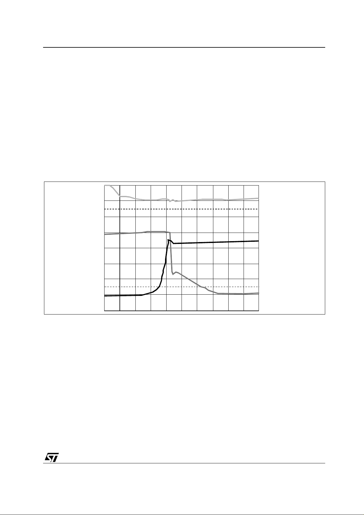
Figure 3: Typical Waveforms During Turn-Off
V
ge
V
CE
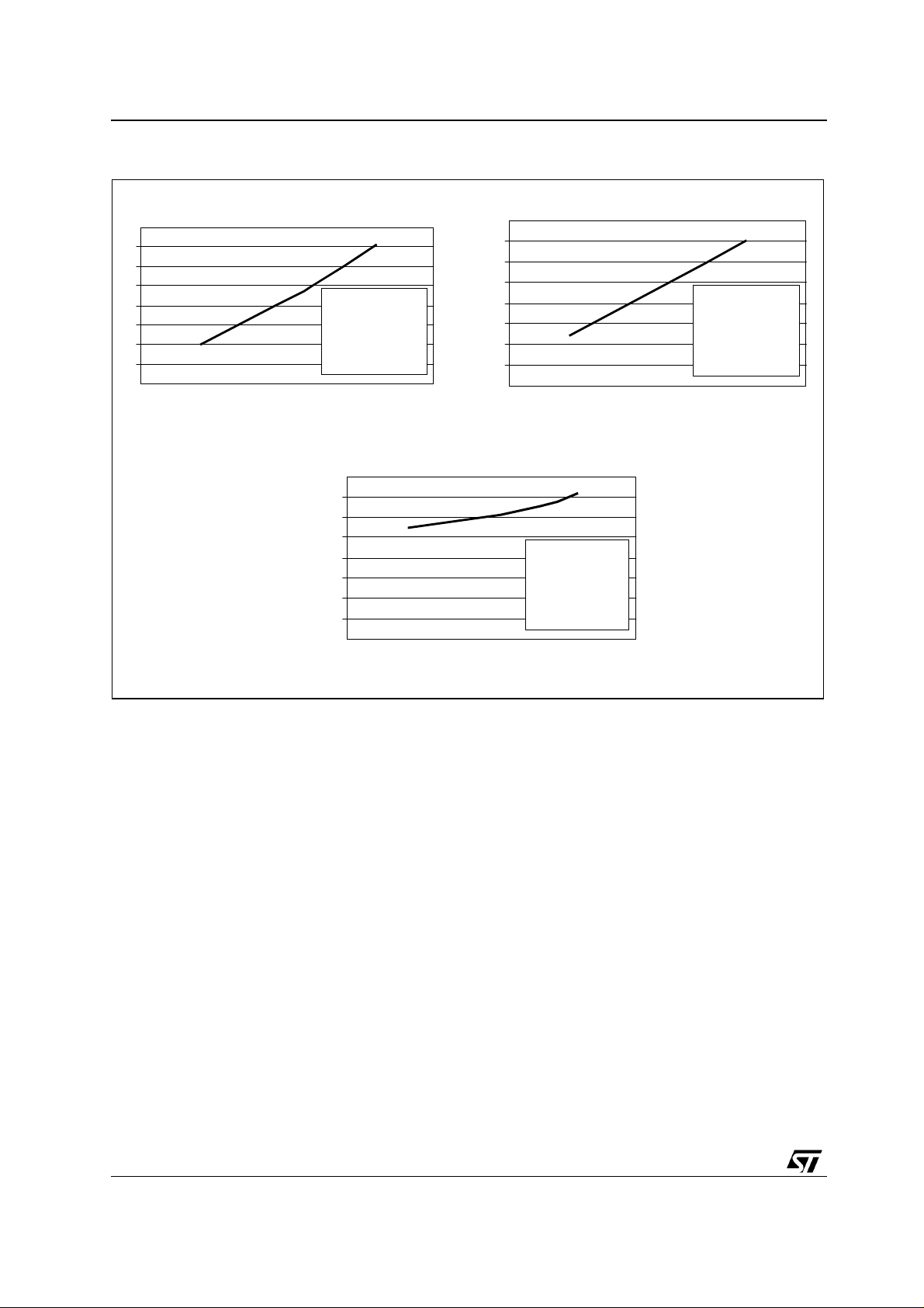
Considering that the tail current is linked to the minority carrier’s recombination its value and shape are
strictly related to the holes’ mobility strictly related to the temperature r eached by the die, I
depending on the temperature reached, it is possible to reduce the undesirable effect of this current
acting on the end equipment design, as indicated in the graphs below, where the tail current (I
behavior related to V
, IC, and TC is depicted (figure 4).
CE
I
C
and VCE. So
C
tail
3/16
)
Page 4
AN1491 - APPLICATION NOTE
Figure 4: I
I
tail
8
7
6
5
4
3
2
1
0
0 5 10 15 20 25
Dependance From IC, TC, and V
tail
(A)
Tc = 100°C
Vce = 400V
Rg = 100Ω
Vge = 15V
IC(A)
4
3.5
3
2.5
2
1.5
1
0.5
0
CE
I
(A)
tail
4
3.5
3
2.5
2
1.5
1
0.5
0
0 100 200 300 400 500
Tc = 100°C
Ic = 10A
Rg = 100Ω
Vge = 15V
VCE(V)
I
(A)
tail
Vce=400°C
Ic = 10A
Rg = 100Ω
Vge = 15V
0 25 50 75 100 125
TC(°C)
5. REVERSE BLOCKING .
When a negative vol tage is applied to the collector then J1 is reverse biased and the de pletion layer
expands to the N- region. This mechanism is fundamental because an excessive reduction of this layer’s
thickness does not obtain a valid blocking capability. On the other hand increasing the dimension of this
region too much consistently elevates the voltage drop.
This second option explains clearly why NPT devices have a higher voltage drop when compared with an
equivalent (equal I
6. FORWARD BLOCKING.
When gate and emitter are shorted and a positive voltage is applied to the collector terminal the P/N- the
J3 junction is reverse biased. Again it is th e depletion layer in the N- drift region that withstands the
voltage applied.
7. LAT CH UP.
IGBT s contains a parasitic PNPN thyristor between the collector and the emitter, as evidenced in figure 1.
Under particular conditions this parasitic device enters in turn on. This causes an i nc rease in the c urrent
flowing between emitter and coll ector, a lose of control of the equivalent MOS FET and gene rally the
disruption of the compon ent. T he turn-o n of the thyristor is k nown as la tch up of the I GBT, more in detail
and speed) PT part.
C
4/16
Page 5
AN1491 - APPLICATION NOTE
the causes of this failure are different and strictly dependent on the status of the device.
In general a static and a dynamic latch up are distinguished by the following:
- Static latch up happens when the device is in full conduction.
- Dynamic latch up takes place only du ring turn-off. This peculiar phenomenon strongly limits the safe
operating area.
In order to avoid this dangerous effect of the parasitic NPN and PNP transistors it is necessary:
- to prevent the turn-on of the NPN part, modifying both the layout and doping level;
- to reduce the overall current gain of the NPN and PNP transistors.
Furthermore the latching current is strictly dependent on the junctions’ temperature since it affects the
current gains of PNP and NPN parts; moreover with an increase of temperature, together with the gains,
the resistance of the P base region becomes higher, aggravating the overall behavior. So particular
attention must be paid by the manufacturer of the parts in order keep distant the maximum collector
current value to the one of the latching current. In general the ratio is in the order of 1 to 5.
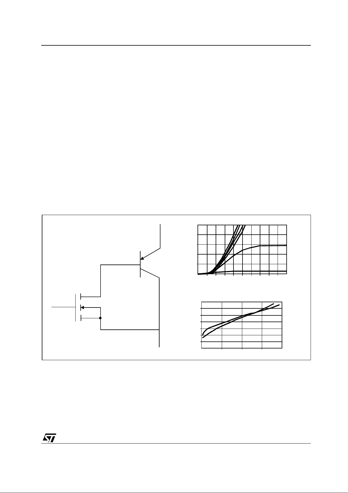
8. FORWARD CONDUCTION CHARACTERISTICS.
Figure 5: Forward Characteris tics And Equi valent Sc hematic Operation
Ice(A)
C
10
8
6
4
2
0
0 0.6 1 1.5 2 2.5 3 3.5 4 4.5 5
V
(V)
CE(sat)
3.5
V
(V)
CE
3
G
2.5
2
1.5
1
E
0.5
0
0 5 10 15 20
I
(A)
C
The IGBT in conduction can be modeled, as a first approximation, as a PNP transistor driven by a Power
MOSFET. Figure 5 only shows the el ements of the structure necessary for the understanding of physic
the device in operation (parasitic elements are not considered).
As showed in the graph rep orting I
as a func tion of VCE (static characteristic), the collector current I
C
does not flow if the vol tage drop between anode and cathode does not exceed 0.7V even if the gate
signal allows the formation of the MOSFET channel, as evidenced in the graphs.
5/16
C
Page 6

AN1491 - APPLICATION NOTE
When the voltage across the channel is greater than VGE-Vth the current i s saturated and the output
resistance becomes infinite. As t he IGBT structure includes both a bipolar and a Power MOSFET, its
temperature characteristics depend on the net effect of the two components that have contrasting
properties. The Power MOSFET ha s a positive temperature coefficient, while the bipolar ’s temperature
coefficient is negative. The figure show s the c hange i n V
two different values of junction temperature. This aspect becomes crucial when it is necessary to parallel
two or more devices and can only be solved by selecting a device to be paralleled, based on V
certain current rate. Sometimes the use of a NPT device for an easy parallel is helpful, but the payback is
an increase of voltage drop when compared with a PT part with the same current level and speed.
9. DYNAMIC CHARACTERISTICS.
The dynamic characteristics indicate the behavior of the device during the switching phases. Considering
the equivalent circuit of the IGBT, it is evident that in order to control the device the MOSFET part must
be driven.
This means the driver system is practically the same as the MOSFET’s one and less complex than the
bipolar’s driver system. As explained before when the positive gate bias is provided via gate, an N
channel is creat ed i n the MOSFET part. I f th e volta ge caused by this f lux i s in th e range of 0.7V the P +/
N- junction is forward biased and the minority carriers are injected in the N- region, creating a hole
bipolar current. The turn-on time is a function of the output impedance of the drive circuit and the applied
gate voltage. It is possible to control the speed of the device by varying the value of the gate resistance
Rg (figure 6), obtaining in this way a different charge velocity of the input parasitic capacitances Cge,
Cgc.
as a function of the collector current f or
CE(sat)
CE(sat)
at a
Figure 6: Rg Effect On dV/dt
I = Cgc = dV/dt
Cgc
C
dV/dt
I
D
dV/dt
Vg = 0
Rg
G
E
Cge
Vg = -5V • Rg = 100 Ohm
In other words, by varying the Rg is it possible to vary the time constant of the parasitic net (reported in
figure) equal to Rg (Cge+ Cgc ) and t hen dv /dt. The gat e dri ve voltage generally adopted and reported in
the datasheets is 15V. In figure 7 waveform s for the switching of an inductive load are reported, while di/
dt as a function of Rg is showed in figure 8, where the effect of gate resistance on the turn on velocity of
the IGBTs is evident.
6/16
Page 7

Figure 7: Rg Effect On dI/dt And Energy In Turn-On
dl/dt (A/µs)
300
AN1491 - APPLICATION NOTE
250
200
150
100
50
0
0 20 40 60 80 100 120
Vce = 400V
Vge = 15V
Tc = 100°C
dl/dt
V
CC
I
RM
I
C
I
C
V
CE
Rg (Ohm)
Therefore, the Rg value strongly impacts the power losses, since its variation also affects the dv/dt
slopes, as shown in figure 8.
Figure 8: dV/dt Dependance On Rg
dV/dt (V/µs)
3000
2500
2000
Vce = 400V
Ic = 10A
Vge = 15V
Tc = 100°C
1500
1000
500
0
0 20 40 60 80 100 120
Rg (Ohm)
During turn-off the behavio r discussed in the equivalent model with a dual cha racteristic of both p ower
MOSFET and BJT devices reemerges again. When the signal t o the gat e decreases to a val ue at which
the Miller effect begins, V
dependent on the driver and affected also by the Cge together with Cgcmiller, the current does not
immediately go to zero b ut assum es t he t ypical shape of a tail, whose length is strictly dependent on the
life times of the minority carriers.
These charges have been injected into the N- region during the positive bias of the device and it is the
main responsible for the worst behavior of IGBTs against MOSFETs in switching. There are several ways
to reduce this effect. For example it is possible to reduce the percentage of the holes injected in turn-on
starts to increase. As explained before after VCE reaches its maximum level,
CE
7/16
Page 8

AN1491 - APPLICATION NOTE
from P+ substrate and in parallel to increase the recombination-speed, by an increase in the dopant level
and the thickness of t he buffer layer. The withdrawal is a reduc tion in current han dling capability due t o
an increase in V
Figure 9: Behavior In Turn-Off With Inductive Load
V
CE
SAFE OPERATING AREA -SOA
The SOA of an IGBT can be div ided into three main area s, distinguished by current and voltage as
indicated in the table below.
and possible associated latching problems.
CE(sat)
I
C
t1
t2
Tj = 125°C
VCE:
100V/div
Turn-off behavior
ICE:
2A/div
Table 1: Voltage Current Physical Limit
Voltage Current Physic al Li m it
Zone 1 High Low Breakdown Voltage
Zone 2 Low High Latch up
Zone 3 High High Power Dissipation
The 3 zones are easily recognizable in figure 10.
The curves describing robustness in forward conduction (Forward Bias Safe Operating Area, FBSOA), in
reverse (Reverse Bias Safe O perating Area, RBS OA), and in s hort circuit (Short Circuit Safe Op erating
Area, SCSOA) are usually available in every datasheet.
More in de tail:
FBSOA
This part of the SOA represents the region where both electron and hole current flows during the turn on
transient. The physical l imit is given by the maximum voltage the device can withstand when the I
saturated, as indicated in figure 10.
is
C
8/16
Page 9

Figure 10: SOA
I
(A)
C
100
10
1µs
100
10
AN1491 - APPLICATION NOTE
(A)
I
C
0.1
10µs
100 1000
10
DC
V
(V)
CE
1
1
1
0.1
VGE = 15V, TC = 100°C
1 10 100 1000
V
(V)
CE
RBSOA
This region represents the turn off transient, when the gate bias is zero or negative but I
is still presen t
C
as the hole current is not extinguished. Here the parasitic transistor, described before, can start the latch
up if the current increases too m uch. When this occurs, the device can no longer be controlled by the
gate. The latest IGBTs do not exhibit this type of behavior, since the triggering of this parasitic SCR can
be made to occur at a current much higher than the one encountered in normal operation (typically I
latch> 5 I
nominal) with appropriate modifications to the structure and the process. Figures 11 and 12
C
show the variation in latch current as a function of junction temperature and gate resistance respectively.
Figure 11: Variation Of Latching Current I
IC(A)
140
With Temperature
latch
120
100
80
60
VCE= 400V
40
Rg = 100 oh m
20
0
Vge = 15V
0 20 40 60 80 100 120
T
(°C)
C
9/16
Page 10

AN1491 - APPLICATION NOTE
Figure 12: Variation Of Latching Current I
IC(A)
140
120
100
80
60
40
20
0
0 20 40 60 80 100 120
latch
With Rg
Rg (Ohm)
VCE= 400V
T
= 100°C
C
Vge = 15V
SCSOA
This is measured by turning on the device at the supply voltage and measuring the maximum time during
which the drive circuit can control the device under test. Figure 13 shows the waveform and the off time
for three devices with equivalent characteristics but manufactured using different technologies.
10. MAXIMUM OPERATING FREQUENCY.
Figure 13: Short Circuit Test
V
CC
VCE= 100V/div
D
CURRENT
PROBE
Rg
C
VgV
I
= 50A/div
C
t
W
V
= 10V/div
G
V
= 10V/div
t
W
D
The switching frequency is a very im portant parameter when choosing a prop er IGBT. This is im portant
since it is strictly relat ed to the power losses of the devi ce. For this reason all silicon pr oducers have
different families tailored for working at different switching frequencies.
In particular STMicroelectronics at the moment offers two different series of products (H, S types), but
other families are in development (K, F, L), giving the customer the possibility to choose the best trade off
in terms of total power losses associated to conduction and switching phases.
In particular it is possible to define the conduction losses as the power dissipated when the current flows
10/16
Page 11

AN1491 - APPLICATION NOTE
and mainly related to V
They could be expressed as: P
CE(sat)
.
cond
= VCE * I
* δ where δ is duty cycle
C
The switching losses are the related to the IGBT’s commutation, they are mainly associated with the total
energy dissipated in operation E
Psw = Ets *
ƒ
and strictly dependent from the frequency ƒ of the end equipment:
ts
The total losses are the sum of the two parts:
P
tot
= P
cond
+ P
sw
At this point it is clear that the overall power dissipation is intrinsically related to two main parameters E
and V
CE(sat)
.
The right trade off between these two variables, strictly related to the IGBTs technology, offers the
customer the option to minimize the overall heat dissipation of the end equipment.
So depending on the frequency of the end equipment and the current level features intrinsically
dependent on application specifications, different parts are chosen in order to minimize the power
consumption.
ts
Figure 14: Main C l uster Fo r End Equipm ent
IGBTs
AUTOMOTIVE
ELECTRONIC
IGNITION
SERVODRIVE
SYSTEMS
HEAD LAMPS
LIGHTING
DIMMER
HIGH FREQ.
BALLAST
HOME
APPLIANCE
WASHING
MACHINE
VACUUM
CLEANER
MICROWAVE
OVEN
FOOD
PROCESSOR
INDUCTION
HEATING
POWER
MANAGEMENT
U PS
MOTOR
CONTROL
WELDING
TELECOM
CONVERTERS
SMPS
Freq kHz
80
40
Automotive
3
Home
Appliances
Lighting
71010 20
Power
Management
30 40 50
I
C
STMicroelectronics represents, especially at current level ideals for motor control, the best trade off
between E
decrease in V
and V
ts
CE(sat)
, as shown in the chart below. Moreover, the dopant typology used allows a
CE(sat)
with the temperature rise, giving a further advantage during the use of the device.
More than this, STMicroele ctronics is now developing new families with different t rade off between E
and V
. A broader range of product is being offered in order to offer our customers and partners true
CE(sat)
independence in design criteria.
ts
11/16
Page 12

AN1491 - APPLICATION NOTE
F
K
V
Figure 15: Trade-Off V
Ets [mJ]
2
1.8
1.6
1.4
1.2
1
0.8
0.6
0.4
0.2
0
Application
Frequency KHz 10 20 40
- E
CE(sat)
ts
IGBT ICX= 7A
S
H,
11.522.53
V
@ 25°C [V]
CE(max)
12/16
Page 13

AN1491 - APPLICATION NOTE
11. DATA SHEET MAIN PARAM ETERS.
11.1 Electric Parameters.
I
-coll ector current
C
The maximum DC current can flow in the devices at a rated temperature (typically 100°C and 25°C).
Icm -pulsed collector current
The peak of the collector current can flow without exceeding maximum junction temperature. This
parameter is strictly related to pulse width, duty cycle and thermal conditions of the device.
Ices -collector cut off current
Maximum collector-emitter leakage current with gate and emitter shorted, under a rated V
CE
value
(usually given @25C and @125C).
Iges –gate emitter leakage current
Maximum gate-emitter leakage current with collector and emitter shorted, under a rated Vge value.
Vces –collector emitter voltage
Maximum voltage b etween collector and em itter, with gate short-circuited with the emitter. This voltage
indicates the physical limit related to the breakdown of the junction between the power terminals.
VBRces -collector emitter breakdown vo ltage
Breakdown voltage between collector and emitter with gate terminal shorted to the emitter one. This
parameter is given at a rated current I
.
C
Vge -gate emitter voltage
Maximum applicable voltage between gate and emitter .
Vgeth -gate emitter threshold voltage
Gate emitter voltage necessary to reach a specified I
V
–collector emitter saturation voltage
CE(sat)
.
C
Collector emitter voltage with a fixed Vge (in general 15V) and for a rated value of collector current. This
13/16
Page 14

AN1491 - APPLICATION NOTE
voltage is usually indicated with Ic f lowing in the device at 25°C and 10 0°C and it represents the v oltage
drop for the rated I
.
C
11.2 Equivalent Capacitances.
Cies -input capacitance
Input capacitance with collector and emitter shorted.
Coes -output capacitance
Output capacitance with gate and emitter shorted.
Cres-reverse transfer capacitance
Collector and gate capacitance.
11.3 Time Parameters.
Tf -fall time
Time requested to reach 10% of the collector nominal current from 90% of its value. This parameter is
fundamental for the understanding of the device’s speed.
Tr -rise time
Time requested to reach 90% of the collector nominal current starting from 10% of its value.
Tdon -turn- on delay time
The time it takes for the collector current to reach 10% of nominal current valu e starting from the time a
forward pulse is applied to the gate.
Tdoff -turn off delay time
The time it takes for V
to reach 10% of the rated value when the voltage’s signal is removed from the
CE
gate.
Tsc-short circuit withstand time
This is the time an IGBT can resist without a ny permanent damage t o the passage of a high valu e of
current when V
=Vces/2, like in the condition of a short circuit in a motor control system. The minimum
CC
value generally requested for a short circuit series is 10µs.
14/16
Page 15

AN1491 - APPLICATION NOTE
11.4 Power Losses Indicators.
Eon –turn on switching losses
Total am ount of energy lost during the turn-off with inductive load. The time interval considered starts
when I
in co-package.
Eoff –turn off switching losses
Total amo unt of energy lost during the turn off with inductive load. The time interval consid ered starts
when V
in co-package.
Ets –total switching losses
Total amount of energy lost during the switching. It is the sum of Eon and Eoff.
ris es fr om zer o up t o t h e ti me VCE decreases to zero. It includes also diode losses when inserted
C
rises from zero up to the time IC decreases to zero. It also includes diode losses when inserted
CE
P
–maximum power dissipation
tot
The maximum power dissipation esteemed when the Tj is at the maximum rated value.
11.5 Thermal Parameters.
Tj -junction temperature
Tem perat ure of the junction. Industry standard range is from -55°C to 150°C.
Tstg –storage temperature
Temperature range for storage and transportation. Industry standard range is from -55°C to 150°C.
R
θjc-Thermal junction to case resistance
Thermal resistance between junction and package. When a diode is present, in the datasheet two values
of R
θjc are indicated, one for the diode and another one for the IGBT.
R
θcs-Thermal case to sink resistance
Thermal resistance between case and sink. It varies with several parameters mainly related to materials
and assembly systems.
Rsa-Thermal sink to ambient resistance
Thermal resistance between heatsink and ambient.
15/16
Page 16

AN1491 - APPLICATION NOTE
Information furnished is b elieved to be accurate a nd reliable. Howe ver, ST Microelectronics a ssumes no resp onsibility
for the consequences of use of such information nor for any infringement of patents or other rights of third parties
which may result from its use. No license is granted by implication or otherwise under any patent or patent rights of
STMicroelectronics. Specification ment ioned in this p ublication are subject to change without notice. This publication
supersedes and repla ces a ll information pre viously su pplied. STM icr oelectro nics pr oducts are not authorized for use
as critical components in life support devices or systems without express written approval of STMicroelectronics.
The ST logo is a registered trademark of STMicroelectronics
© 2001 STMicroelectronics - Printed in Italy - All rights reserved
STMicroelectronics GROUP OF COMPANIES
Australia - Brazil - Canada - China - Finland - France - Germany - Hong Kong - India - Isreal - Italy - Japan - Malaysia -
Malta - Morocco - Singapore - Spain - Sweden - Switzerland - United Kingdom - U.S.A.
http://www.st.com
16/16
 Loading...