


AN1485
APPLICATION NOTE
MDmesh™ PERFORMANCE EVALUATION IN A
CONTINUOUS MODE PFC BOOST CONVERTER
G. Belverde - M. Melito - A. Raciti - M. Saggio - S. Musumeci
1. ABSTRACT
A new high voltage MOSFET structure is presented which results in static as well as dynamic
performances far ahead conventional Power MOSF ET devices. The impact of the particular features of
the device is analyzed and quant ified in a c ase stu dy regarding a DC-DC boost conv erter, which is used
in a power factor corrector (PFC) converter. Results obtained from the analysis of the electrical and
thermal behavior of the component in the specific are discussed.
2. INTRODUCTION.
Standard technology for high voltage suited Power MOSFETs has been dramatically improved, thus the
physical limit in terms of reduction of the device’s on-state resistance is going to be reached. In fact, such
a device parameter is strongly affected by the drain resistivity value, which is designed according to the
requirements of the high v oltage blocking capability. Recently, an innovative concept of Power M OS FET
design has been proposed that is able to enhance t he dev ice’s performance [1 , 2]. In these new devices
the charge balance makes the electric field constant over the whole drain volume in spite of t he low
resistivity in this conducting region. In breakdown conditions the electric field has a value almost equal to
the critical one for silicon.
In this paper the main issues of process technology are shortly recalled and discussed. The static and
dynamic characteristics are shown aiming to evaluate the advantages of the new device in comparison to
standard Power MOSFETs having both the same rated voltage and current carrying capability. Finally,
the evaluation of the performance is foc used on in a spec ific application, in particular in a bo ost-based
power factor corrector (PFC) converter.
3. TRENDS ON POWER MOSFET (MDmesh™) DEVICE TECHNOLOGY .
A revolutionary three-dimensional design of the drain device volume is at the basis of the MDmesh™
MOSFET device. The extensio n of the top strip layout to the whole drain volume, by p-doped column
insertion under device stripes, allows a strong resistivity reduction of the c onduction n-doped layer and
an impressive decrease of the device’s on-state resistance when com pared to a convent ional MOSFE T
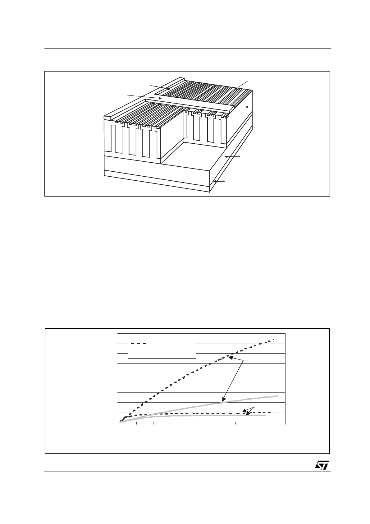
[1]. The cross section of an MDmesh™ device is depicted in figure 1, where both the strip layout and the
column insertion under the de vice stripes are shown. As a consequence of this approach, the known
theoretical limit of performanc e for vertical Power MOS FET devices decreases. I n fact, the MDmesh™
MOSFET overcomes this limit allowing a mass production of devices with improved perform ance and
reduced area. For example, a 500V MDmesh™ MOSFET is almost three times smaller than a
conventional MOSFET having the same blockin g voltage.
November 2001
1/14
AN1485 - APPLICATION NOTE
SUBSTRATE
DRAIN
10
Vgs=10V
Figure 1: Three-Dimensional Cross Section Of MDmes h™ Device
N-SOURCE
P-MESH
GAT E
FINGER
BACK METAL
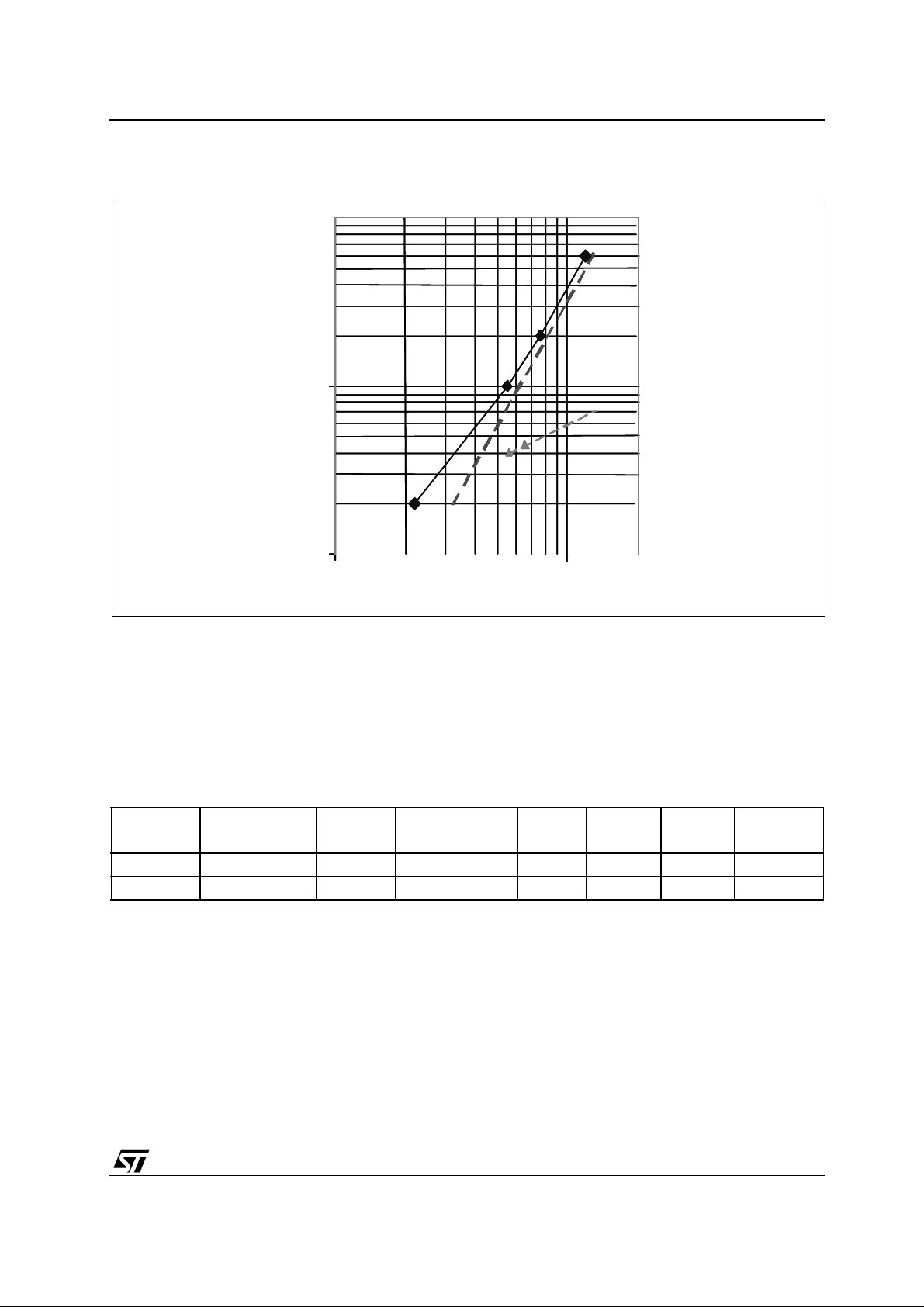
The static output characteristics o f a n M Dme sh ™ MO SF ET i n c om parison to a s tandard dev ice wit h the
same silicon area a re reported in figure 2. Moreover, simulation anal ysis and theoretical consi derations
show that in MDmesh™ t echnology the device’s on-state resistance increases linearly as funct ion of t he
breakdown voltage, according to the traces shown in figure 3. The direct consequenc e of this result is
that the extension of the M Dmesh™ MOSFETs towards higher blocking voltage values will continually
increase the advantages of this technology . The fabrication of a 1000V MDmesh™ MOSFET will require,
as expected from the design, a silicon area seven (7) times smaller than a conventional M OSFET with
the same on-state resistance and blocking voltage capability. This will cause a package reduction and a
major improvement in any appli cation based on these devices, as c onsequenc e of the st rong reduction
obtained on volume and weight of the board. The extension to very high blocking voltage of MDmesh™
MOSFETs will represent a real revolution in high voltage converter applications.
Figure 2: Static Output Characteristics (I/V Curves) Of An MDmesh™ (STP12NM50) And A
St andard MO S FET Having Equal Si l icon Area
18
16
14
MDmesh™
Std Technology
12
10
Ids (A)
8
6
4
Vgs=6V
2
0
0123456789
Vds(V)
2/14
AN1485 - APPLICATION NOTE
Figure 3: Standard MOSFET and MDmesh™ Depend ence Of On-State Resistance As A Function
Of The Breakdown Voltage
1000
1000
t
t
i
i
m
m
i
i
l
l
l
l
a
a
e
e
d
d
i
i
n
n
o
o
c
c
i
i
l
l
i
i
S
S
D
D
M
M
T
T
E
E
]
]
2
2
o
o
i
100
100
Ron Area [mΩ cm
Ron Area [mΩ cm
10
10
100 1000
100 1000
i
t
t
n
n
e
e
v
v
n
n
o
o
C
C
y
y
g
g
o
o
l
l
o
o
hn
hn
c
c
e
e
t
t
l
l
a
a
n
n
F
F
S
S
O
O
M
M
Breakdown Voltag e [V]
Breakdown Voltag e [V]
Another important feature obtained b y the proposed approach reduction of the intrinsic c apacitances [3],
in comparison to the one of a more t raditional device, as seen in table 1. In switch m ode power supply
(SMPS) and PFC applications the reduction of the intrinsic parasitic capacitance allows a com mutation
time decrease, thus enabling the increase of the switching frequency. As known, this will result in
important reduction of both volume and cost of the reactive components used to filter the output and/or
electrical quantities.
Table 1. Main Characteristics Comparison
Part Number BV
DSS
[V]
R
DS(on)
[Ohm]
@ 25°C
Ciss
[pF]
Coss
[pF]
Crss
[pF]
Package
Standard STW15NB50 >500 0.36 2600 330 40 TO-247
MDmesh™ STP12NM50 >500 0.38 1000 160 25 TO-220
4. SWITCHING CHARACTERISTICS.
A characterization of the new device has been carried out in order to give evidence to the good switching
performance of the new de vice. The silic on area shrin king allowed by the M D m esh™ techn ology ad ds a
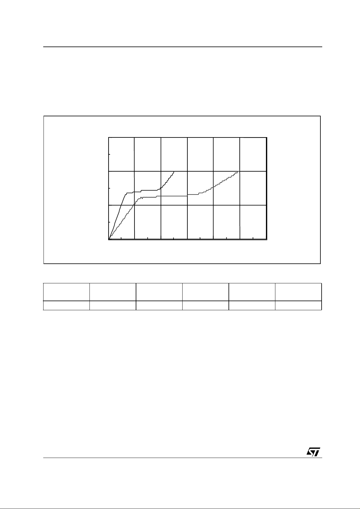
further benefit to the device’s gate charge due to the parasitic capacitance reduction. Th e gate charge
comparison of figure 4 refers to two devices with equal rated electrical characteristics. At the driving
voltage of 10V the MDmesh™ requires a gate charge reduced by a factor of 3.5 in respect to the
traditional counterpart, at a drain current of 12A and a drain-source voltage of 200V. The charge stored in
the input capacitance is reduced from 50nC (STW15NB50) t o 25nC (STP12NM50). This immediately
suggests to the end-user an effective driving loss reduction. Moreover, as a consequence, this feature
allows an improvement of the performance during the switching transients in comparison with
conventional devi ces [4 ].
3/14
AN1485 - APPLICATION NOTE
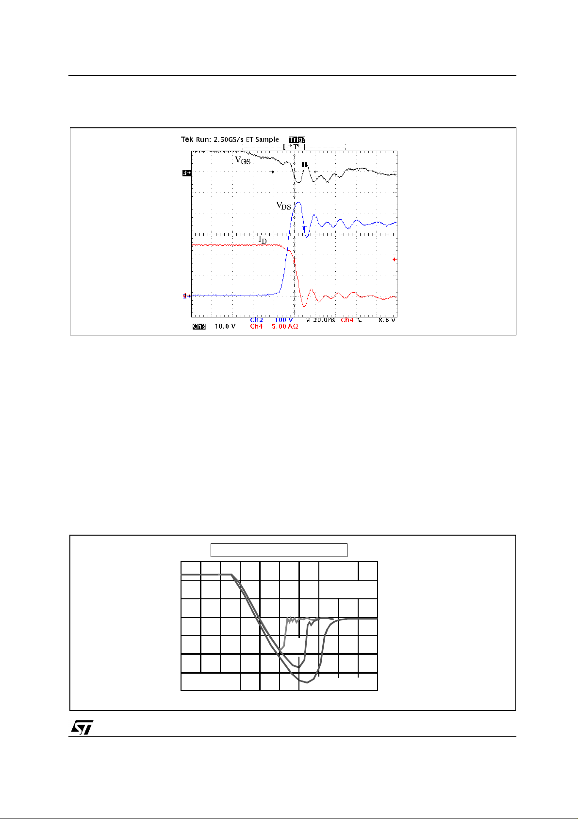
The switching transient evaluation has been performed at room temperature on inductive load at several
gate-driving conditions. The main quantities of a typical c ommutation, in hard switching conditions on
inductive load, are reported in table 2, while in figure 5 the traces of an experimental turn-off switching
transients are shown.
Figure 4: Gate Charge Behavior Of Two Different Power MOSFET Devices
Gate Charge
15
10
(V)
GS
V
STP12NM50
5
STW14NB50
0
0 10 20 30 40 50 60
Charge [nC]
Table 2. MDmesh™ Typical Switching Quantities (RG=4.7Ohm)
E
off
[µJ]
28.6 10.8 7.6 888.9 36.84 33.6
t
fall
[ns]
t
rise
[ns]
di/dt
[A/ns]
dv/dt
[V/ns]
t
delay
[ns]
4/14
AN1485 - APPLICATION NOTE
Figure 5: Current And Voltage Traces During A Typical Turn-Off Transient Of An MDmesh™
(V
=100V/div, VGS=10V/div, ID=5A/div, t=20ns/div)
DS
5. INTRINSIC BODY-DRAIN DIODE.
In some industrial equipment, which requires a conv erter configuration with bi-directional switches, the
intrinsic diode of the MOSFET device may be used as antiparallel diode if its own characteristics are
adequate. In order to optimize the design, the performance of the body-drain diode of the new device has
been investigated. In particular, the switching behavior of t he body-drain diode has bee n widely tested.
The well-established technique of Platinum implanting has been performed in order to reduce the reverse
recovery time (t
) of the body-drain diode b y reducing the carrier lifetime. Platinum implanting a cts as a
rr
lifetime killer by introducing a mi d gap center in the silicon. By increasing the Platinum dose ( Φ) a t
reduction is observed. The obtained experimental waveforms during a reverse recovery transient for
three devices with different Platinum doses are reported in figure 6 that is related to a current slope di/dt
equal to 100A/ms.
Figure 6: Reverse Recovery Of The Body-Drain Diode In Case Of Different Platinum Doses
(ID=5A/div, t=100ns/div)
Vds=100V, di/dt=100A/µs, Id=12A
Φ1 < Φ2
Φ2
Id (A)
Φ1
rr
BV
DSS
=600V
No lifetime killer
100ns/div
5/14

AN1485 - APPLICATION NOTE
6. MDmesh DEVICE IN A PFC CONVERTER APPLICATION.
Power MOSFET devices are very suitable for many power converter applications, operating at high
frequency, which have been proposed aiming to develop SMPS with high power factor value. In these
applications the dev ices experience high voltage, l ow current and high freque ncy. In particular, a PFC
circuit has been cons idered, wh ich is based on a boost conv erter to pology in o rder t o obtain h igh p ower
factor. The control of the converter is performed by an L4981A integrated circuit that behaves as a
continuous mode PFC controller and uses the technique of the average current control [5]. A prototype of
the converter has been prepared and its simplified schematic is shown in figure 7.
Figure 7: A Simplified Block Schematic Of The Control Stage And Power Stage Of The PFC
Application
I
OUT
V
R
0
L
PWM
Modulat or
_
+
_
+
V
ref
Sinusoidal
Referenc e
Controller
Circuit
I
0
C
IN
Current
Sensing
L
V
IN
1
0
snubber
Current
Error
Amplifier
I
D
D
C
_
+
K
x
z=xy
y
Voltage
Mult ipli er
Error
Amplifier
The constraints adopted to design the PFC converter are the following:
• Input AC voltage from universal mains VIN=88V up to 264V, freque ncy 50/60Hz;
• DC regulated output voltage VOUT=400V;
• Full load output ripple voltage DVr<16V;
• Rated output power POUT=200W;
• Maximum output voltage VO(max)=450V;
• Switching frequency in the range of 100-200kHz;
• Maximum inductor current ripple DIL=35%;
• Input power factor PF>0.99;
• Total harmonic distortion of the line current < 5%.
OUT
The values of some passive components of the converter circuit are reported in table 3 in the case of two
different switching frequencies, namely 100kHz and 200kHz. In the structure of the P FC converter a
6/14

AN1485 - APPLICATION NOTE
snubber circuit has been used for the switching device in order to reduce its power losses and to
maintain a low value of the dv/dt looking for the EMI requirements. According to the design criteria of the
RCD snubber, and by imposing for the drain voltage to h ave a ri se time t
=40ns, the capacitor v alue has
r
been fixed at C=350pF (630V) while the resistance value depends on the working frequency.
The value is R=1.8kOhm at 100kHz , and 680Ohm at 200kHz. The efficiency of the power converter is
mainly dependant on the power losses of both the switching device and the snubber circuit.
Table 3. Passive Component Values Selected For Two Switching Frequencies
Switching Frequency
[kHz]
L
0
[mH]
C
IN
[nF]
C
[µF]
0
100 0.9 220 100
200 0.45 114 100
7. THERMAL BEHAVIOR OF THE POWER SWITCH.
The total power losses P
of a switching device can be split into the following components: the
t
commutation power losses (turn-on and turn-off) and the on-state power losses:
PtPON= P
The turn-on losses, which dep end on both the diode choice and the dv/ dt imposed by the R
++ 1()
OFFPcon
G(on)
, can be
designed as a trade off between the power losses and the EMI requirements. The snubber circuit
reduces the turn-off switching power losses, which, in turn, cannot be included. The main contribute to
the device power losses is given by the conduction component that depends on the R
of the device.
DS(on)
With reference to the symbol used in figure 7, the rms current on the inductor is given by:
P
OUT
-------------
I
=2()
0
ηV
IN
where η is the converter efficiency. The current reaches a maximum value at the minimum value of the
main voltage V
at twice the frequency of the main line, the
. From relation (2) and by cons idering t hat the dut y c ycle of t he sw itch is m odul ate d
IN,MIN
rms
current in the MOSFET can be calculated by (as given in
[6]):
P
OUT
-------------
I
=3()
D
ηV
V
IN
-------------
k
V
IN
OUT
,
Lf
R,
s
0
where the function
k
operates as a reduction factor. Finally the on-state power losses P
can be
con
evaluated by:
con
DS on()ID
R
=4()
P
2
At constant output power this value changes according to the variation of the main voltage. The
maximum value of this rms current occurs in the case of the lowest value of the main voltage V
IN,MIN
(88V). In the case study a typical figure for the efficiency η is in the range 0.88-0.90. The maximum peak
value of the device current is given by:
∆I
0
------- -
I
Dmax,
I
+=5()
0max,
2
7/14

AN1485 - APPLICATION NOTE
where ∆I0 is the current ripple on the inductor.
Calculating from (5) for the I
gives a curren t of 4A in the case of 200W output of the converter.
D,max
Moreover, accounting for the peak of the current due to the reverse recovery of the diode, and by adding
a suitable safe margin, a switching device with a rated current carrying capability of 8A has been
selected. The breakdown voltage of the device is determined according to the following relation:
BV
DSSVOUT
where the voltage V
is a suitable value ranging between 10% and 15% of the maximum output voltage.
m
With the above constraints, we need a device having at least BV
∆VrV
++≥ 6()
m
=500V.
DSS
Finally , the freewheeling diode has been specified as a 6A, 600V fast diode, with a reverse recovery time
=25ns.
t
rr
8. JUNCTION TEMPERA TURE CALCULATION.
A dynamic characterization of the Power MOSFET has been carried out. The device is very fast and has
a good switching performance. The current and voltage waveforms of the device during a typical turn-off
transient are reported in figure 8. We can observe that the rise time of the drain voltage in the case
shown is coherent with the design constraints on the voltage slope.
Figure 8: T urn-Off Switching Transient In The PFC Converter At A Main Voltage Of 88V (V
=2A/div, E=1kVA/div, t=50ns/div)
div, I
D
=100V/
DS
The thermal behavior has been performed by a set-up measurement shown in figure 9, where the
thermal model of the device is also indicated. In steady state condition we measured the heatsink
temperature at a different value of the input voltage, and namely at 88V, 110V and 220V. The junction
temperature is higher than the heatsink temperature and can be estimated by the following procedure.
8/14

AN1485 - APPLICATION NOTE
Figure 9: Block Schematic Of The Measurement System To Determine The Heatsink T emperature,
As Well As The Steady State Thermal Model Of The Device
TAR
th, S, ARth, C, SRth, J, CTJ
Temper atur e
Measur em e nt
Firstly, the power loss is calculated:
THTA–
-------------- ------
= 7()
P
D
R
th H A,()
where T
is the measured heatsink temperature, TA is the ambient temperature fixed at 27°C, and R
H
th,H,A
is the thermal resistance of the heatsink established at 7°C/W. Then the junction temperature is
calculated by:
R
+()+=8()
thCH,()
where T
and R
T
jTHPDRthJC,()
is the junction temperature, R
J
is the thermal resistance between the case and the heatsink. The results for the two
th(C,H)
is the thermal resistance between the junction and the case
th(J,C)
switching frequencies considered are reported in table 4. Other results obtained for the same output
power and the results of the experimental tests done at different voltages and frequencies are reported in
table 5. The tests have been carried out at the beginning of the experiments (room temperature, T=27°C)
and in steady state conditions.
Table 4. Heatsink And Junction Temperatures For Different Voltage And Frequency Values
V
[V]
IN
T
H
[°C]
P
[W]
D
T
J
[°C]
100kHz
88 92 9.28 107
110 70 6.14 80
220 46 2.71 50
220kHz
88 98 10.14 1 14.5
1 10 75 6.86 86.2
220 49 3.14 54.1
9/14

AN1485 - APPLICATION NOTE
Table 5. Results Of The Experimental Tes ts At Different Voltages And Frequencies
T
H
[°C]
V
[V]
IN
I
IN
[A]
P
IN
[W]
V
OUT
[V]
I
OUT
[A]
P
[W]
OUT
η%
100kHz
27 88 2.4 211 393.7 0.485 191 90.5
92 2.472 217 395.8 0.488 193.1 89
27 110 1.88 206.6 394.6 0.484 190.9 92.4
70 1.931 21 2.3 397.1 0.49 194.6 91.8
27 220 0. 934 20 4.5 396.8 0.49 194.4 95.1
46 0.948 20 6.3 397 0.489 194.1 94.7
200kHz
27 88 2.487 217.8 395 0.482 190. 4 87.4
98 2.577 22 6.7 395 0.483 190.8 84.2
27 110 1.957 211.9 398 0.489 19 5 92
75 2.016 22 0.7 398 0.499 198.6 90
27 220 0. 959 211 398.5 0. 49 195.3 93
49 0.968 213 398 0.49 195 91.6
9. HARMONIC DISTORTION.
The main results for the converter from the stand point of the harmonic content are reported in table 6,
where the term A-THD% stands for the total-harmonic-distortion (in percentage) of the main current, and
PF is the power factor. The test-rig used to obtain the data given in table 6 is depic ted in figure 10. T he
better performance of the PFC is at a main voltage of 110V and 60Hz. In figure 11 we can s ee the near
zero-value of the phase shift between the input waveforms of the voltage and current. The PF measured
in such a case is 0.999, as reported in table 6. Finally, the voltage and current traces in a whole switching
cycle of the MDmesh™ device are reported in figure 12a, 12c. The test conditions are switching
frequency 200kHz and main voltage V
IN, MIN
=88V.
Figure 10: Experimental Set-Up To Measure The Harmonic Distortion And The Power Factor
V
0
main
AC Source
And Power Meter
t
Oscilloscope
Vprobe
Iprobe
Multimeter
PFC
C
O
LOAD
10/14
Controller
IC

AN1485 - APPLICATION NOTE
Figure 11: Experimental Traces Of The Input And Output Waveforms (VIN=110V, ƒ=60Hz,
=200kHz, VIN=100V/div, V
f
s
=100V/div, I
OUT
=500mA, IIN=1A/div, t=2ms/div)
OUT
Figure 12a: Working Cycles Of The Power MOSFET Device In Loaded Conditions @ 200kHz
(V
=100V/div, ID=2A/div, t=1µ s/ div)
DS
11/14

AN1485 - APPLICATION NOTE
Figure 12b : The MDme sh™ Turn-off In Loa ded Cond itions (VDS=100V/div, ID=2A/div, E=1kVA/div,
t=50ns/div)
Figure 12c: The MDmesh™ Turn-on In Loaded Conditions (V
t=50ns/div)
=100V/div, ID=2A/div, E=1kVA/div,
DS
12/14

Table 6. Performance Of The PFC As A Non-linear Switching Load
AN1485 - APPLICATION NOTE
V
[V]
IN
ƒ
s
[Hz]
I
IN
[A]
PF A - THD% V
OUT
[V]
∆V
OUT
[V]
f = 100kHz
88 60 2.472 0.9984 4 393.7 13
110 60 1.931 0.994 2.4 394.6 13
220 50 0.948 0.9976 4.9 396.8 14
f = 200kHz
88 60 2.577 0.9986 3.7 393 15
110 60 2.016 0.997 1.7 394.6 14
220 50 0.968 0.9981 4.4 397 15
10. DISCUSSION OF THE RESULTS.
The new device features good performance in the experimental tests. In particular, the device works very
well in terms of efficiency and harmonic distortion in a typical power conversion application, like the PFC.
However, it is worth it to note that equivalent results may be obtained by traditional Power MOSFETs
having a larger silicon area. In fact, an equivalent standard device should have two times the area of the
device presented here. The consequence is a smaller package for the MDmesh™ device than a
standard MOSFET, and a lower cost. However, in such a case at equal power losses the smal ler d evice
will assume a greater junction temperature. Obviously we are presuming different total thermal
resistance, which is the c ase. O n the other hand, the new equivalent device has a high current density,
good switching performance and on-state losses comparable to standard MOSFETs.
11. CONCLUSION.
In this paper an extende d charac terization of a new class of P ower MO SFE Ts has been performed. The
advantages and drawbacks relative to the new device has been highlighted. An important improvement
in comparison with equivalent convent ional devices consists i n the area reduction of the silicon. As a
consequence the current density of the proposed device is higher than the current density of a standard
one. The switching performa nce is im proved due to the lower parasitic capacitance and t he lo w on-state
resistance adds major advantages in terms of forward voltage drop.
13/14

AN1485 - APPLICATION NOTE
REFERENCES:
[1] M. Saggio, D. Fagone, S. Musumeci “MDmesh™: Innovative Technology For High Voltage Power
MOSFETs”, Conf. Rec. ISPSD 2000, T oulouse, France, May 22-25 2000.
[2] L. Lorenz , L. Zverev, A. Mittal, J. Hancock “CoolMOS – A New Approach Towards System
Miniaturization And Energy Saving” Conf. Rec. IEEE IAS 2000; Roma, Italia, October 2000.
[3] F. Di Giovanni, A. Magri “STripFET: Innovative Low Voltage Power MOSFETs” Proceedings of the
Power Conversion Intelligent Motion PCIM 1998 Conference, June 1998, Santa Clara, CA.
[4] S. Musumeci, A. Raciti, A. Testa, M. Melito, A. Galluzzo “Switching Behavior Improvement Of
Insulated Gate Controlled Devices” IEEE Transactions On Power Electronics, Vol. 12, No. 4, July 1997,
pp.645-653.
[5] J. Rajasgopalan, F.C. Lee, P. Nora ”A General Technique For Derivation O f Average Current Mode
Control Laws For Single-Phase Power-Factor Correction Circuits Without Voltage Sensing” IEEE
Transactions On Power Electronics, Vol. 14, No. 4.
[6] G. Commandatore, U. Moriconi “Designing A High Power Factor Pre-regulator With The L4981
Continuous Mode” Application Note AN628/0795 by STMi croelectron ics.
Information furnished is b elieved to be accurate a nd reliable. Howe ver, ST Microelectronics a ssumes no resp onsibility
for the consequences of use of such information nor for any infringement of patents or other rights of third parties
which may result from its use. No license is granted by implication or otherwise under any patent or patent rights of
STMicroelectronics. Specification ment ioned in this p ublication are subject to change without notice. This publication
supersedes and repla ces a ll information pre viously su pplied. STM icr oelectro nics pr oducts are not authorized for use
as critical components in life support devices or systems without express written approval of STMicroelectronics.
The ST logo is a registered trademark of STMicroelectronics
© 2001 STMicroelectronics - Printed in Italy - All rights reserved
STMicroelectronics GROUP OF COMPANIES
Australia - Brazil - Canada - China - Finland - France - Germany - Hong Kong - India - Isreal - Italy - Japan - Malaysia -
14/14
Malta - Morocco - Singapore - Spain - Sweden - Switzerland - United Kingdom - U.S.A.
http://www.st.com
 Loading...