

Page 1

AN1476
APPLICATION NOTE
LOW-COST POWER SUPPLY FOR HOME APPLIANCES
INTRODUCTION
In most non-battery applications, the power to the microcontroller is supplied by using a stepdown transformer, which is then rectified, filtered and regulated. However, in many smaller
low-cost applications, the cost of the transformer becomes the key factor in the system. Under
these circumstances, the step-down transformer is normally not used in order to reduce the
cost as well as the size. The power supply is a simple one-way rectifier with very few components. The output voltage is regulated by using a 5.6V zener diode. Despite its simplicity and
low cost, it is still able to deliver enough current to the microcontroller and application circuits.
The purpose of this application note is to present the basic principle and cost analysis of the
various power supply circuits for home appliance applications.
AN1476/0904 1/8
1
Page 2
LOW-COST POWER SUPPLY FOR HOME APPLIANCES
1 BASIC CIRCUITS
1.1 TRANSFORMER POWER SUPPLY
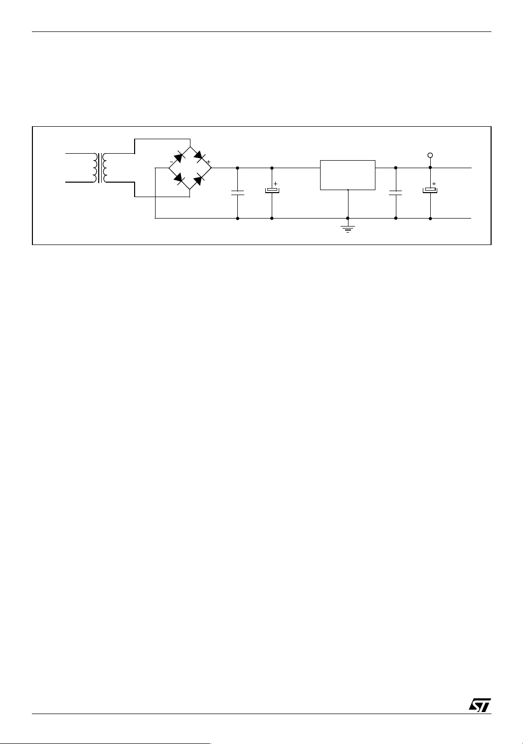
Figure 1. Transformer Power Supply Diagram
T1
N
1
3
4
2
L
4
1N4003*4
3
2
100nF
C1
C2
470uF/35V
U2
78L05
IN
GND
OUT
C3
10nF
VCC
C4
100uF/16V
Figure 1. describes how to obtain a 5V DC voltage from the AC power line. In this circuit, the
AC voltage drops down on the transformer’s secondary winding. A rectifier bridge with 4 diodes is used to convert the alternating AC voltage to a continuous DC voltage supply. A filter
capacitor is added after the rectifier bridge in order to decrease the DC voltage ripple. The
78L05 triple terminal voltage regulator provides a very stable output and high current.
The advantages of this solution are:
■ Power Supply is isolated from the AC line voltage,
■ Power Supply can deliver high current (up to 100 mA for 78L05),
■ The ripple of DC voltage will be small.
However, the disadvantages of this solution are also obvious:
■ Much more expensive than transformerless power supplies,
■ Power supply size is bigger due to the transformer and other components.
2/8
2
Page 3
LOW-COST POWER SUPPLY FOR HOME APPLIANCES
1.2 CAPACITIVE POWER SUPPLY
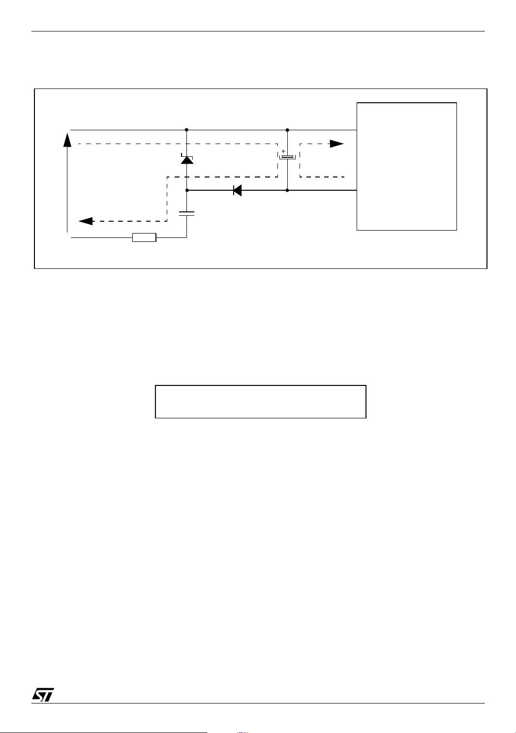
Figure 2. Capacitive Power Supply Diagram
N
D1
V
Iin
R
L
470/0.5W
5.6V
D2
1N4148
C1
470nF/400V
Cs
220uF/16V
Iout
Vdd
MCU
Vss
Figure 2. describes the capacitive power supply. In order to have a constant voltage across
capacitor Cs, the average value of the input current (I
of the output current (I
). Current through this capacitor (Cs) flows during only the positive
OUT
) must be equal to the average value
IN
half cycle of the supply and during the negative half cycle it flows through the zener diode.
Input current (I
) is a half-wave current, whose value is given by the following equation (R and
IN
Cs can be disregarded as the impedance offered by these is negligible in comparison to C1 ):
I
INav
V
--------------------------------------=
peak
2πfC1⋅⋅
π
Here Vpeak/PI = Average(dc equivalent) voltage in one cycle.
π.f.C1 = impedance offered ( neglecting R and Cs) . The voltage rating of C1 should be
2.
greater than Vpeak as it is charged up to Vpeak.
Resistance and Capacitance(Cs) significance:
Cs has to be charged upto 5.6 V. So the voltage rating should be more than 5.6V. This capacitor reduces ripples from the output supply. As one tries to withdraw more and more current,
the ripples will be increased. The high value of Cs would reduce the ripples from the supply up
to a certain limit.
Resistace(R) limits the current through the zener diode. The value of R should be such that
Vpeak/R is more than the current limit of the zener.
To ensure the delivery of enough current in the worst conditions (Vpeak, f and C at minimum),
the average output current, sunk by the MCU, must match the following conditions (capacitor
3/8
Page 4

LOW-COST POWER SUPPLY FOR HOME APPLIANCES
value has ±20% accuracy), for a 220V / 50Hz supply:
I
OUTav
2 200
⋅⋅⋅<
V()98Hz()
0.8C
F()
Note: For a 110V/60Hz calculation, replace 200V and 98Hz with 100V and 118Hz respectively.
The advantages of this solution are:
■ The transformer is removed and the cost is significantly reduced.
■ Power Supply size is smaller
■ Maximum output current values are proportional with the AC capacitor values.
Removing the transformer optimizes the cost. As a result, the power supply is not isolated
from the AC line voltage and the microcontroller is powered directly from the AC line.
In a capacitive power supply, the input current is mainly determined by the capacitor value on
the AC line. The energy is stored in capacitor C on the positive half-wave cycle and can be restored on the other half-wave cycle. In order to obtain a higher minimum output current, increase the capacitor value on the AC line.
Table 1 gives the maximum average output current values in relation to the various AC capac-
itor values.
Table 1 Maximum MCU Average Current Values for a 220V / 50Hz supply
AC Capacitor Value Max. MCU Average Current Value
220 nF 4.9 mA
330 nF 7.3 mA
470 nF 10.4 mA
680 nF 15 mA
1µF 22.1mA
4/8
Page 5

LOW-COST POWER SUPPLY FOR HOME APPLIANCES
1.3 RESISTIVE POWER SUPPLY
Figure 3. Resistive Power Supply Diagram
N
D1
5.6V
C1
220uF/16V
Vdd
MCU
Iout
V
Vss
D2
Iin
L
R
18K/2W
1N4007G
Figure 3. describes the resistive power supply. As shown in the diagram, the current passing
through resistor R in the conductive half cycle is mainly dependent on the value of the resistor
because the reactance of the capacitors is much less than that of the resistors. The value of
the current through resistor R is therefore given by the following equation:
V
---=
I
R
The current through resistor R is a half-wave current, the average current value is given by the
following equation:
Vpeak
I
INav
----------------=
R π×
In order to have a constant current through capacitor C1, the input current must be equal to
output current. In the worst conditions (V
at minimum and R at maximum), the average
PEAK
output current, sunk by the MCU, must match the following conditions:
I
OUTav
200
------------------------------------------ -
3.14 1.1 18
⋅⋅
V()
2⋅
4.5mA=<
kΩ()
The advantages of this solution are:
■ As with the capacitive power supply, the transformer is removed and the cost is significantly
reduced.
5/8
Page 6

LOW-COST POWER SUPPLY FOR HOME APPLIANCES
■ The circuit is very simple and the cost is even less expensive than the capacitive power
supply.
In the resistive power supply, the input current is determined by the resistor value on the AC
line. Therefore, the power consumption of this resistor is very high. In order to reduce the
power consumption on this resistor, it is better to increase the resistor value. But the maximum
output current will be decreased accordingly.
The disadvantages of resistive power supply are:
■ Maximum average output current is limited and can not be adjusted easily.
■ Power consumption on the resistor is high.
■ Power supply is not isolated from the AC line.
6/8
Page 7

LOW-COST POWER SUPPLY FOR HOME APPLIANCES
2 COST ANALYSIS OF A POWER SUPPLY WITH/WITHOUT TRANSFORMER
2.1 COST ANALYSIS
Table 2 Cost Analysis of a Power Supply with/without Transformer
Components
1.1 VA Transformer 1.50 1 1.50 0 - 0 1N4003 Diode 0.05 4 0.20 0 - 0 L7805 0.15 1 0.15 0 - 0 470 µF/35V 0.30 1 0.30 0 - 0 100 µF/16V 0.20 1 0.20 0 - 0 1N4148 Diode 0.03 0 - 1 0.03 0 470 nF/400 V 0.30 0 - 1 0.30 0 1N4007 Diode 0.05 0 - 0 - 1 0.05
18K/2W Resistor 0.03 0 - 0 - 1 0.03
5.6V Zener Diode 0.02 0 - 1 0.02 1 0.02
220 µF/16V 0.20 0 - 1 0.20 1 0.20
Total 2.35 0.55 0.30
1) Prices are listed in US dollars (year 2000). All prices are based on > 1000 unit quantities.
Unit
Price
1)
Transformer
Qty
Power Supply
Qty
Power Supply
Capacitive
Qty
Power Supply
Resistive
As shown above, the cost of the transformer power supply is much higher than without a transformer power supply.
3 CONCLUSION
To correctly design the power supply, the following conditions should be taken into account:
■ The maximum currents required by the application circuits,
■ Overall cost/performance evaluation.
7/8
Page 8

LOW-COST POWER SUPPLY FOR HOME APPLIANCES
“THE PRESENT NOTE WHICH IS FOR GUIDANCE ONLY AIMS AT PROVIDING CUSTOMERS WITH INFORMATION
REGARDING THEIR PRODUCTS IN ORDER FOR THEM TO SAVE TIME. AS A RESULT, STMICROELECTRONICS
SHALL NOT BE HELD LIABLE FOR ANY DIRECT, INDIRECT OR CONSEQUENTIAL DAMAGES WITH RESPECT TO
ANY CLAIMS ARISING FROM THE CONTENT OF SUCH A NOTE AND/OR THE USE MADE BY CUSTOMERS OF
THE INFORMATION CONTAINED HEREIN IN CONNEXION WITH THEIR PRODUCTS.”
Information furnished is believed to be accurate and reliable. However, STMicroelectronics assumes no responsibility for the consequences
of use of such information nor for any infringement of patents or other rights of third parties which may result from its use. No license is granted
by implication or otherwise under any patent or patent rights of STMicroelectronics. Specifications mentioned in this publication are subject
to change without notice. This publication supersedes and replaces all information previously supplied. STMicroelectronics products are not
authorized for use as critical components in life support devices or systems without express written approval of STMicroelectronics.
The ST logo is a registered trademark of STMicroelectronics.
All other names are the property of their respective owners
© 2004 STMicroelectronics - All rights reserved
STMicroelectronics group of companies
Australia – Belgium - Brazil - Canada - China – Czech Republic - Finland - France - Germany - Hong Kong - India - Israel - Italy - Japan -
Malaysia - Malta - Morocco - Singapore - Spain - Sweden - Switzerland - United Kingdom - United States of America
www.st.com
8/8
 Loading...