

Page 1

AN1474
APPLICATION NOTE
ST92F150 A ND ST92F120 PROBLEM RESOLUTION
GUIDELINES
by Microcontroller Division Applications
INTRODUCTION
The ST92F12 0 and ST 92F15 0 are par t of the sa me fa mily of pow erful m icrocon trollers fr om
STMicroelectronics, featuring single voltage flash memory and an innovative E3prom concept.
This document gives guidelines on resolving several common application problems that have
been reported by ST Application Engineers.
Testflash features
The testflash features are described in the ST92F120 and ST92F150 datasheets.
Located in a reserved flash area, the TestFlash contains the bootcode which performs the
E3prom initialization, provides the possibility to program the flash by In System Programming
(refer to the application note
then jumps to the start address application code via the reset vector.
AN1450 ST9 Flash Programming
for a detailed description) and
AN1474/1001 1/10
1
Page 2

ST92F150 AND ST92F120 PROBLEM RESOLUTION GUIDELINES
1 EXTERNAL WATCHDOG ROUTINE
During the bootcode execution (from 12.5 ms up to 75ms if an aborted E3prom write operation
is detected), a code routine provided by the user may be executed to refresh an external
watchdog.
The routine address offset is located at addresses 0x000006h and 0x000007h while the segment where the routine is located has to be written in 0x000009h.
You must fill the word at the address 0x000006h with 0xffffh if your application does not use an
external watchdog.
Startup file example (usually called crtbegin.spp) :
.org 0x06
.word 0xffff
Refer to the application examples provided with the ST9+ User Guide.
1.1 PROBLEM DESCRIPTION
The application is not executed at all and it is not possible to communicate by ISP with the programming board.
1.2 ANALYSIS
When the chip is read directly with the programming board, the contents of addresses
0x000006h and 0x000007h is not equal to 0xFFh.
These addresses in the application code are not equal to 0xFF whereas an external watchdog
routine is not provided.
1.3 RESOLUTION
Modify the application code as mentioned at the beginning of this section and erase and reprogram the device.
There is no way to modify this chip by ISP, it has to be unsoldered.
2/10
2
Page 3
ST92F150 AND ST92F120 PROBLEM RESO LUTION GUIDELINES
2 ST92F120 RESET VECTOR
One of the powerful features provided by the ST9 Flash device family is the possibility to upgrade the application code by downloading and programming through an I/O interface on the
MCU (refer to the application note
AN1275 In Application Programming for the ST 92F120
a detailled description).
In case of a parasitic reset during the flash upgrade operation, the application must be able to
recover safely by executing the bootloader code.
To perform this, the bootloader is present in the flash sector where the application starts, the
one pointed to by the reset vector. This sector must never be erased.
This is why the reset vector is always located in the smallest sector.
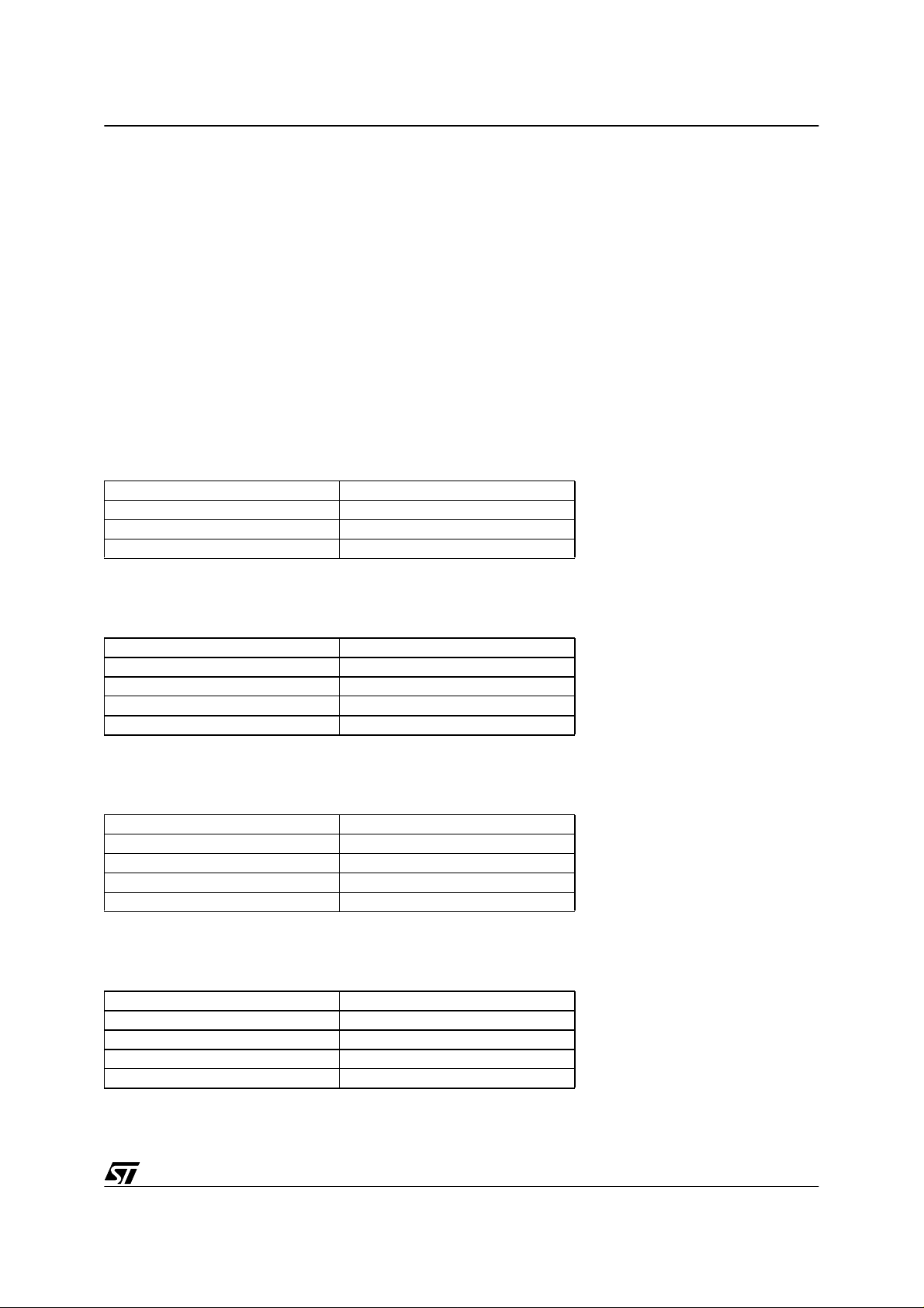
ST92F120 60Kbyte Flash device map
Sector Size
F0 4 Kbyte
F1 48 Kbyte
F2 8 Kbyte
for
ST92F120 128Kbyte Flash device map
Sector Size
F0 64 Kbyte
F1 48 Kbyte
F2 8 Kbyte
F3 8 Kbyte
ST92F150 60 Kbyte Flash device map
Sector Size
F0 8 Kbyte
F1 8 Kbyte
F2 32 Kbyte
F3 12 Kbyte
ST92F150 128Kbyte Flash device map
Sector Size
F0 8 Kbyte
F1 8 Kbyte
F2 48 Kbyte
F3 64 Kbyte
3/10
Page 4

ST92F150 AND ST92F120 PROBLEM RESOLUTION GUIDELINES
2.1 SPECIAL RESET VEC TOR MAPPING IN ST 92F120 128KBYTE FLASH DEVICE
The reset vector is located at the beginning of Sector F0, at address 0x000000, in all
ST92F150 and ST92F120 microcontrollers but one : the ST92F120 128Kbyte Flash device. In
this device, the reset vector is located in 0x01E000h, at the begining of the sector F3.
The ST92F120 emulator has the same behaviour as the ST92F120 60Kbyte Flash device : its
reset vector is located in 0x000000h, at the beginning of Sector F0.
So, how to emulate an ST92F120 128Kbyte Flash device ?
There are two possibilities :
1. The application startup code is located in Sector F3 and an instruction is added to jump
from Sector F0 to Sector F3. This jump is executed by the emulator but not by the final
application.
2.The application startup code is located in F3 and an instruction is added to jum p from Sector F3 to Sector F0. This jump is executed by the final application but not by the emulator.
2.1.1 Jump from Sector F0 to F3
If the application starts in Sector F3 (for example if you are developing an IAP bootloader), a
line of code has to be added in Sector F0 to jump to the reset vector. This way the emulator will
jump to the beginning of the application, executing just one more instruction than the chip.
4/10
Page 5

ST92F150 AND ST92F120 PROBLEM RESO LUTION GUIDELINES
Example, resetf0.spp :
;Use this file only when emulatin g the code
#include "config.spp"
#include "define.h"
PROGRAMMING_MODEL
.section .init
;emulator reset vector redirectio n
.word __ResetF0
.org 0x06 ;external watchdog routine v ector
.word 0xffff
.org 0x0a
.proc __ResetF0
__ResetF0:
jps seg(__Reset), sof(__Reset )
.endproc __ResetF0
This file must be defined in the makefile.mak as a spp source file.
Example :
# Give here th e name of the C/SPP/ASM source files used in the application
C_SRC = main.c
SPP_SRC = resetf0.spp
ASM_SRC =
# Give here the name of the strat up files used in the application
STARTUP_SRC = crtbegin.spp crtend .spp
5/10
Page 6

ST92F150 AND ST92F120 PROBLEM RESOLUTION GUIDELINES
The “init” section of the resetf0.spp file must be loaded in Sector F0 in the scriptfile.ld.
Example :
MEMORY
{
FLASH0 : ORIGIN = 0x000000, LENGTH = 6 4K, MMU = IDPR0
FLASH1 : ORIGIN = 0x010000, LENGTH = 4 8K, MMU = IDPR1
FLASH2 : ORIGIN = 0x01c000, LENGTH = 8K
FLASH3 : ORIGIN = 0x01e000, LENGTH = 8K, MMU = IDPR2
RAM : ORIGIN = 0x200000, LENGTH = 4K, MMU = IDPR3
EEPROM : ORIGIN = 0x220000, LENGTH = 1K,
REGFILE (t) : ORIGIN = 0x00, LENGTH = 0xb0 /* Groups 0 to 0x0B */
}
SECTIONS
{
.initF0 :
{ resetf0.spp(.init) } > FLASH0
.init :
{ *(.init) } > FLASH3
.text :
{ *(.text) } > FLASH3
.fini :
{ *(.fini) } > FLASH3
Remark :
If the compact memory model is selected, the compiler will generate the following warn ing
message :
appli.u(.init): warning: code section not in the same segment as section `.initF0'
appli.u(.text): warning: code section not in the same segment as section `.initF0'
It is normal, because in the compact memory model, all the application code must be located
in the same 64Kbyte segment. But, since the added jump is the first instruction executed and
the only one in Segment F0, there is no impact on the execution of the application.
6/10
Page 7

ST92F150 AND ST92F120 PROBLEM RESO LUTION GUIDELINES
2.1.2 Jump from Sector F3 to F0
If the application does not start in Sector F3 (8Kbyte) but in F0 (64Kbyte) you must add a jump
from Sector F3 to Sector F0. This jump will not be executed by the em ulator.
Example, resetf3.spp :
#include "config.spp"
PROGRAMMING_MODEL
.section .init
.word ResetF3
ResetF3:
jps seg(__Reset), sof(__Reset)
This file must be defined in the makefile.mak as a spp source file.
Example :
# Give here th e name of the C/SPP/ASM source files used in the application
C_SRC = main.c
SPP_SRC = resetf3.spp
ASM_SRC =
# Give here the name of the strat up files used in the application
STARTUP_SRC = crtbegin.spp crtend .spp
The “init” section of the resetf3.spp file must be loaded in Sector F3 in the scriptfile.ld.
7/10
Page 8

ST92F150 AND ST92F120 PROBLEM RESOLUTION GUIDELINES
Example :
MEMORY
{
FLASH0 : ORIGIN = 0x000000, LENGTH = 6 4K, MMU = IDPR0
FLASH1 : ORIGIN = 0x010000, LENGTH = 4 8K, MMU = IDPR1
FLASH2 : ORIGIN = 0x01c000, LENGTH = 8K
FLASH3 : ORIGIN = 0x01e000, LENGTH = 8K, MMU = IDPR2
RAM : ORIGIN = 0x200000, LENGTH = 4K, MMU = IDPR3
EEPROM : ORIGIN = 0x220000, LENGTH = 1K,
REGFILE (t) : OR IGIN = 0x00, LENGTH = 0xb0 /* Groups 0 to 0x0B */
}
SECTIONS
{
.initF3 :
{ resetf3.spp(.init) } > FLASH3
.init :
{ *(.init) } > FLASH0
.text :
{ *(.text) } > FLASH0
.fini :
{ *(.fini) } > FLASH0
Remark :
If the compact memory model is selected, the compiler will generate the following warn ing
message :
appli.u(.init): warning: code section not in the same segment as section `.initF3'
appli.u(.text): warning: code section not in the same segment as section `.initF3'
It is normal, because in the compact memory model, all the application code must be located
in the same 64Kbyte segment. But, since the added jump is the first instruction executed and
the only one in Segment F3, there is no impact on the execution of the application.
8/10
Page 9

ST92F150 AND ST92F120 PROBLEM RESO LUTION GUIDELINES
2.2 PROBLEM DESCRIPTION
We are using ST92F120 128Kbyte flash devices from several lots.
The application w or ks fine w ith the o lde st ones but is n ot executed at a ll with the new ones.
The microcontroller seems to be halted.
2.3 ANALYSIS
Before tracecode V99080 027 (mid -2000), th e reset vector of the ST92 F120 128 Kbyte flash
device was located in 0x000000h, which was not suitable for In Application Programming
needs. It has been changed and the reset vector is now located in 0x01E000h.
2.4 RESOLUTION
Add a jump from Sector F3 to Sector F0.
9/10
Page 10

ST92F150 AND ST92F120 PROBLEM RESOLUTION GUIDELINES
"THE PRESENT NOTE WHICH IS FOR GUIDANCE ONLY AIMS AT PROVIDING CUSTOMERS WITH INFORMATION
REGARDING THE IR PRO DUCT S IN OR DER FO R THEM TO SAV E TIME . AS A RES ULT, STMIC ROEL ECTR ONI CS
SHALL NOT BE HELD LIABLE FOR ANY DIRECT, INDIRECT OR CONSEQUENTIAL DAMAGES WITH RESPECT TO
ANY CL AIM S AR IS IN G FR OM T HE CO N TENT OF S UC H A NO TE A ND /O R T HE U SE M AD E BY C US TO ME RS O F
THE INFORMATION CONTAINED HEREIN IN CONNEXION WITH THEIR PRODUCTS."
Information furnished is believed to be accurate and reliable. However, STMicroelectronics assumes no responsibility for the consequences
of use of such information nor for any infringement of patents or other rights of third parties which may result from its use. No license is granted
by implic ation or otherwise under any patent or patent ri ghts of STM i croelectr oni cs. Spec i fications mentioned i n this publication are subje ct
to change without notice. This publication supersedes and replaces all information previously supplied. STMicroelectronics products are not
authorized for use as cri tical comp onents in life support dev i ces or systems wi thout the express written approv al of STMicroel ectronics.
The ST logo is a registered trademark of STMicroelectronics
2001 STMicroelectronics - All Rights Reserved.
STMicroelectronics Group of Compan i es
http://www.s t. com
Purchase of I
2
C Components by STMicroelectronics conveys a license under the Philips I2C Patent. Rights to use the se components in an
2
I
C system i s granted pro vi ded that the sy stem conforms to the I2C Standard Specification as defined by Philips.
Australi a - B razil - Canada - China - Finl and - France - Germany - Hong Kong - Ind ia - Israel - Italy - Japan
Malaysi a - M al ta - Morocco - Singapore - Spain - Sw eden - Switz erland - United Kingdom - U.S.A.
10/10
 Loading...