

AN1451
APPLICATION NOTE
L6208 FULLY INTEGRATED TWO PHASE
STEPPER MOTOR DRIVER
by Domenico Arrigo, Vincenzo Marano and Thomas Hopkins
Modern motion control applications need more flexibility that can be addressed only with specialized IC
products. The L6208 is a full y i ntegr ated steppe r motor dr iv er IC speci ficall y developed to drive a wide r ange
of two phase (bipolar) stepper motors. This IC is a one-chip cost effective solution that includes several
unique circuit design features. These features, including a decoding logic that can generate three different
stepping sequences, allow the device to be used in many applications inc luding microstepping. The prin cipal
aim of this development project was to produce an easy to use, fully protected power IC. In addition several
key functions such as protection circuit and PWM current control drastically reduce external components
count to meet requirements for many different applications.
1 INTRODUCTION
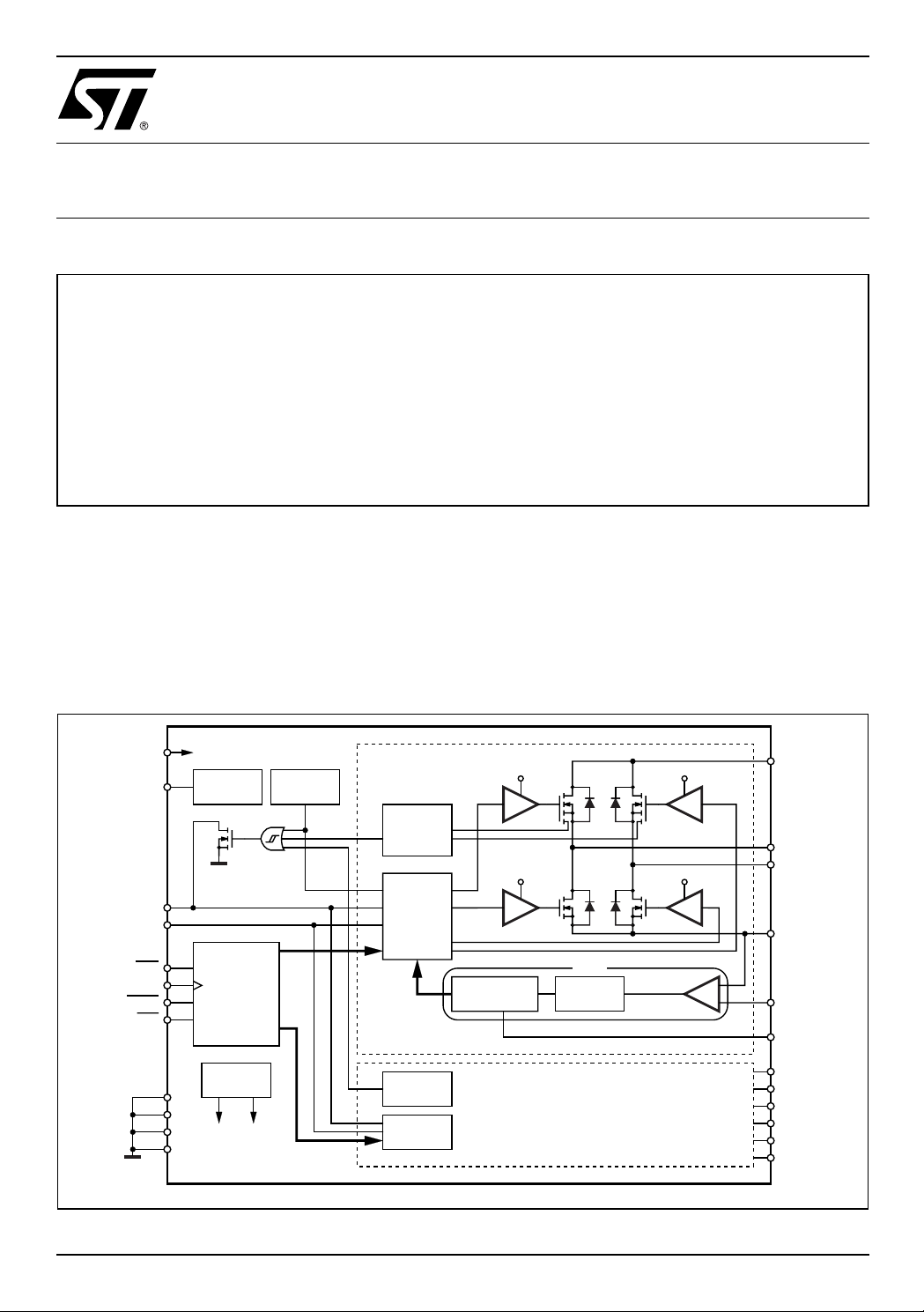
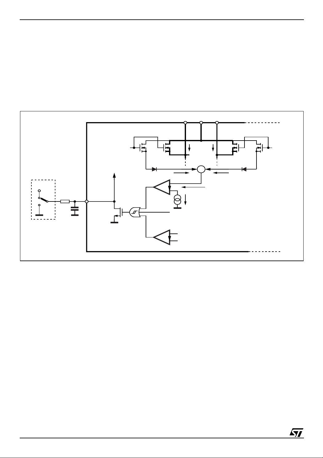
The L6208 is a highly integrated, mixed-signal power IC that allows the user to easily design a complete motor
control system for two-phase bipolar stepper motors. Figure 1 shows the L6208 block diagram. The IC integrates eight Power DMOS, a centralized logic circuit which implements the phase generation and a constant
t
PWM current control technique (
OFF
other added features for safe operation and flexibility.
Quasi-Synchronous mode
) for each of the two phases of the motor plus
Figure 1. L6208 block diagram.
V
BOOT
V
CONTROL
HALF/FULL
CLOCK
RESET
CW/CCW
GND
GND
GND
GND
CP
EN
V
BOOT
CHARGE
PUMP
STEPPING
SEQUENCE
GENERATION
VOLTAGE
REGULATOR
5V10V
L6208
THERMAL
PROTECTION
OCD
OCD
V
V
BOOT
OVER
A
B
CURRENT
DETECTION
GATE
LOGIC
OVER
CURRENT
DETECTION
GATE
LOGIC
10V 10V
PWM
ONE SHOT
MONOSTABLE
MASKING
TIME
V
BOOT
SENSE
COMPARATOR
BRIDGE A
BRIDGE B
+
-
D01IN1226
SA
OUT1
OUT2
SENSE
VREF
RC
A
V
SB
OUT1
OUT2
SENSE
VREF
RC
B
A
A
A
A
B
B
B
B
October 2003
1/43

AN1451 APPLICATION NOTE
Table of Contents
1 INTRODUCTION................................................................................................................................ 1
2 DESIGNING AN APPLICATION WI TH L620 8 ...................................................................................3
2.1 Current Ratings........................................................................................................................3
2.2 Voltage Rating s and Operating Range ....................................................................................3
2.3 Choosing th e Bulk Capacitor....................................................................................................5
2.4 Layout Considerations.............................................................................................................6
2.5 Sensing Resisto r s.............................. ......................................................... ..................... ....... .8
2.6 Charge pump external components.........................................................................................9
2.7 Sharing the Charge Pump Circuitry .......................................................................................10
2.8 Reference Voltage for PWM Current Control.........................................................................11
2.9 Input Logic pins......................................................................................................................12
2.10 EN pin....................................................................................................................................12
2.11 Program mab le off-time Monost able......................................................................................13
2.11.1 Off-time Selection and minimum on-time ........................................................................15
2.11.2 Decay Modes ............................................................................... ..... ....... ....... ..... ...........16
2.12 Over Current Protection........................................................................................................18
2.13 Power Managem ent..............................................................................................................21
2.13.1 Maximum output current vs. selectable devices..............................................................22
2.13.2 Power Dissipation Formulae for different sequences......................................................22
2.14 Choosing the Decay Mode....................................................................................................25
2.15 Choosing the Step ping Sequence. ........................................................................................26
2.16 Microstepping........................................................................................................................27
3 APPLICATION EXAM PL E.............................. ......................................................... .........................30
3.1 Decay mode, sensing resistors and reference voltage..........................................................30
4 APPENDIX - EVALUATI ON BO ARD S...................................................................... .......................31
4.1 PractiSPIN............................................................................. .................................................31
4.2 EVAL6208N ...........................................................................................................................33
4.2.1 Important Not e s......... ................................... ......................................................... ....... ....34
4.2.2 Thermal Impedance .........................................................................................................34
4.3 EVAL6208PD.........................................................................................................................38
4.3.1 Important Not e s......... ................................... ......................................................... ....... ....39
4.3.2 Thermal Impedance .........................................................................................................39
5 REFERENCES.................................................................................................................................43
2/43
AN1451 APPLICATION NOTE
2 DESIGNING AN APPLICATION WITH L6208
2.1 Current Ratings
With MOSFET (DMOS) devices, unlike bipolar transistors, current under short circuit conditions is, at first approximation, limited by the R
and the two V
and VSB pins are rated for a maximum of 2.8A r.m.s. and 5.6A peak (typical values), corre-
SA
of the DMOS themselves and could rea ch ve ry high values . L6208
DS(ON)
sponding to a total (for the whole IC) 5.6A rms (11.2A peak). These values are meant to avoid damaging metal
structures, including the metal lizati on on the die and bond w ires. In prac tical appl ications , though, maxi mum allowable current is less than these values, due to power dissipation limits (
see
Power Management
The device has a built-in Over Current Detection (OCD) that provides protection against short circuits between
the outputs and between an output and ground (
see
Over Current Protection
section
).
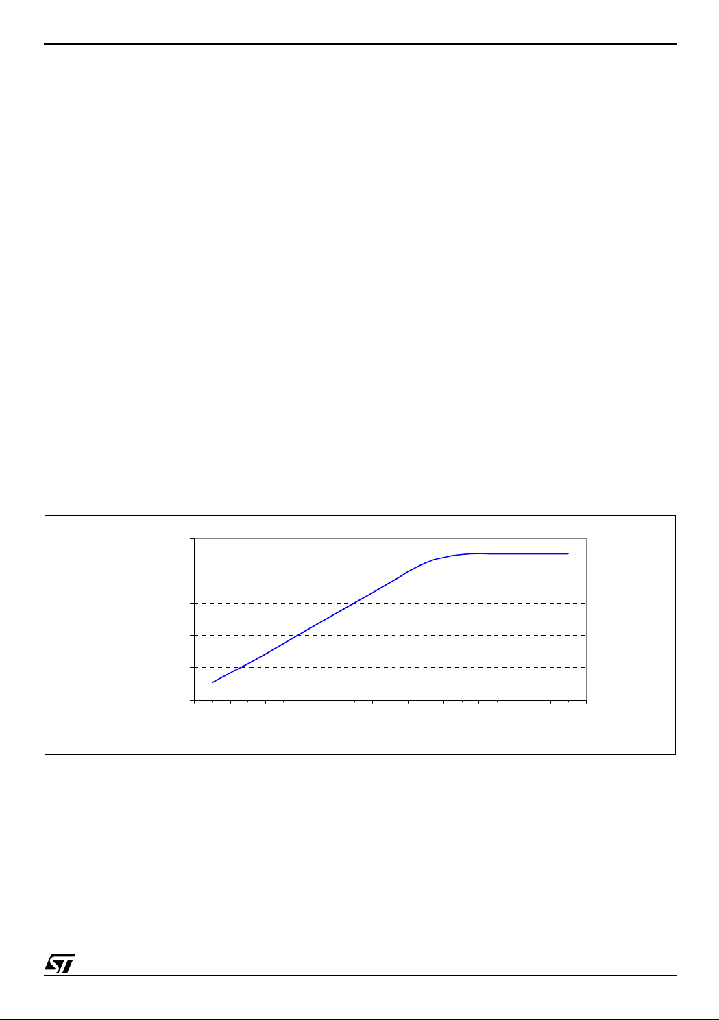
2.2 Voltage Ratings and Operating Range
The L6208 requires a single supply voltage (VS), for the motor supply. Internal voltage regulators provide the
5V and 10V required for the internal circuitry. The operating range for V
undesirable low sup ply vol tage an
voltage falls below 6V; to resume normal operating conditions, V
Under Voltage Lock Out
(
UVLO
must then exceed 7V. The hysteresis is pro-
S
vided to avoid false intervention of the UVLO function during fast V
DMOS's R
is a function of the VS supply voltage. Actually, when VS is less than 10V, R
DS(ON)
affected, and this is particularly true for the High Side DMOS that are driven from V
is 8 to 52V. To prevent working into
S
) circuit shuts down the dev ice when suppl y
ringings. It should be noted, however, that
S
DS(ON)
supply. This supply is
BOOT
obtained through a charge pump fr om the internal 10V supply, which will tend to r educe i ts output v oltage when
V
goes below 10V. Figure 2 shows the supply voltage of the high side gate drivers (V
S
supply voltage (V
).
S
- VS) versus the
BOOT
Out
pins
section
is adversely
).
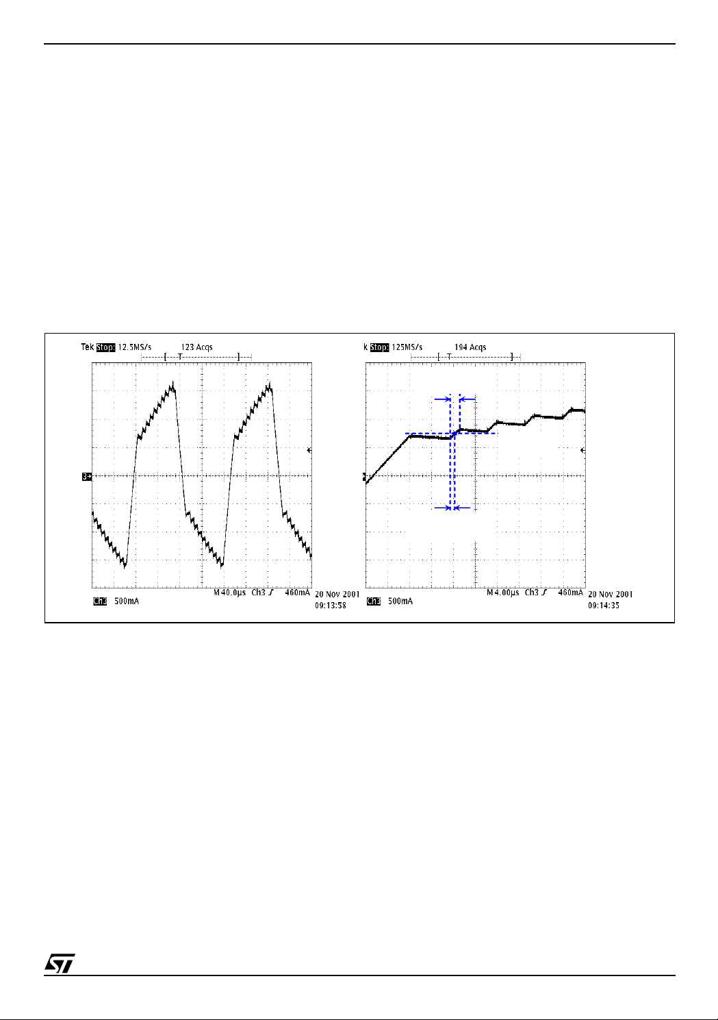
Figure 2. High side gate drivers supply voltage versus supply volta ge.
8
7.6
V
BOOT
- V
[V]
7.2
S
6.8
6.4
6
8 8.5 9 9.5 10 10.5
VS [V]
Note that VS must be connected to both VSA and VSB since the bootstrap voltage (at V
pin) is the same for
BOOT
the two H-bridges. The integrated DMOS have a rated Drain-Source breakdown voltage of 60V. However V
should be kept below 52V, since in normal working conditions the DMOS see a Vds voltage that will exceed V
supply. In particular, when using the
off during dead-time) the
SENSE
PCB path from the pin to GND. This spike is followed by a stable negative voltage due to the drop on R
One of the two
OUT
pins of the bridge sees a similar behavior, but with a slightly larger voltage due to the for-
fast decay
mode, at the beginning of the off-time (when all the DMOS are
pin sees a negative spike due to a not negligible parasitic inductance of the
SENSE
ward recovery time of the integrated freewheeling diode and the forward voltage drop across it (see Figure 3).
Typical duration of this spike is 30ns. At the same time, the other
OUT
pin of the same bridge sees a voltage
S
S
.
3/43

AN1451 APPLICATION NOTE
above VS, due to the PCB inductance and voltage drop across the high-side (integrated) freewheeling diode,
as the current reverses direction and flows into the bulk capacitor. It turns out that, in fast decay, the highest
differential voltage is observed between the two
and this must always be kept below 60V [3]. The same high voltage condition exists when a step is made and
the direction of current flow reverses in the bridge.
OUT
pins of the same bridge, at the beginning of the off-time,
Figure 3. Currents and voltages during the
ESR
Bulk Capacitor
Equivalent Circuit
ESL
PCB Parasitic
Inductance
R
*I+V
SENSE
F(Diode)
R
SENSE
dead time
*I
SENSE
at the beginning of the
V
S
OUT
2
OUT
1
Dangerous
High Differential Voltage
PCB Par a s i ti c
R
SENSE
Inductan ce
off-time
VS+V
F(Diode)
.
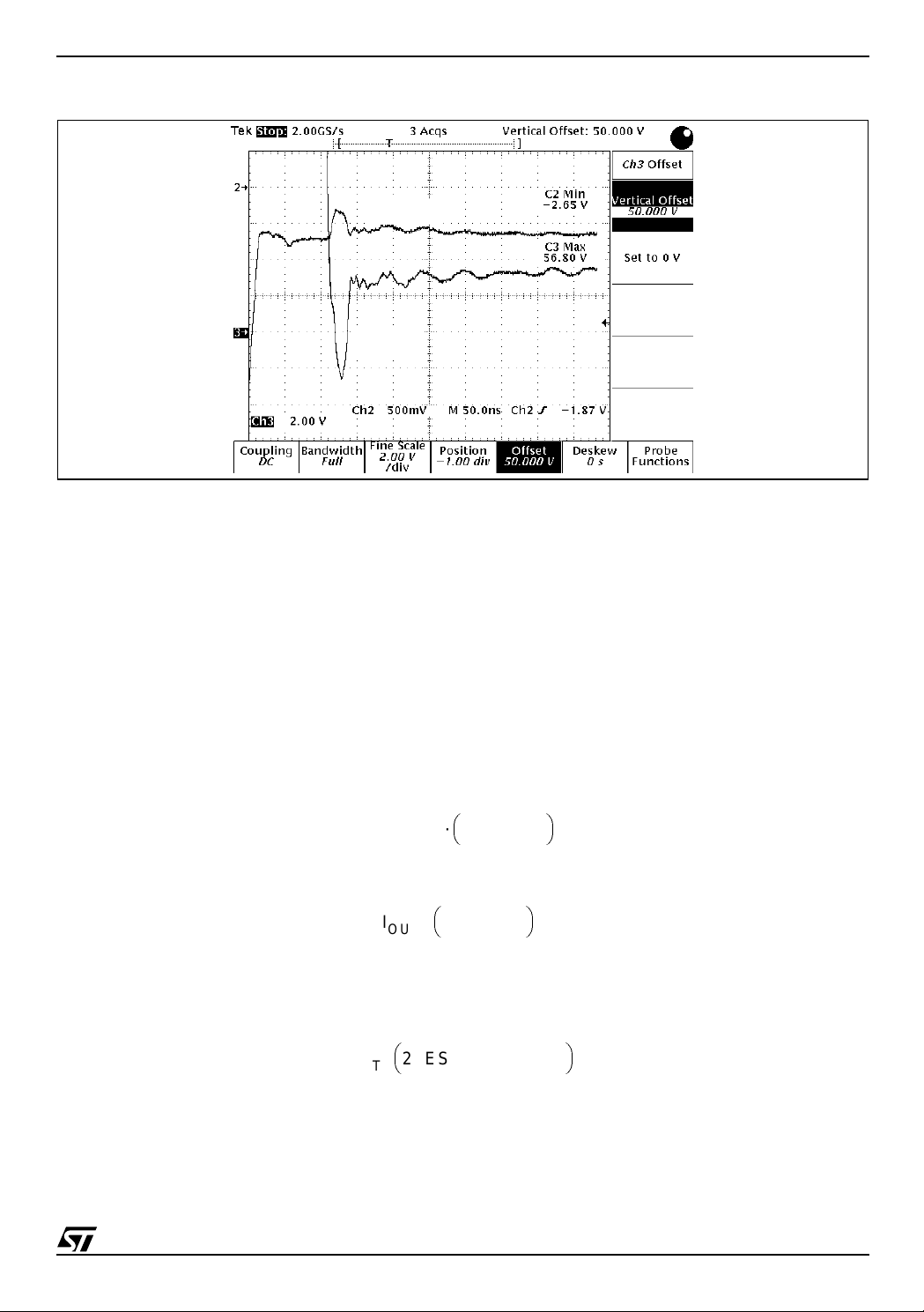
Figure 4 shows the voltage waveform s at the two OUT pins referring to a pos sible pr actical situ ation, with a peak
output current of 2.8A, V
ground spike amplitude is -2.65V for one output; the other
= 52V, R
S
= 0.33Ω, TJ = 25°C (approximately) and a good PCB layout. Below
SENSE
OUT
pin is at about 57V . In these conditions, total
differential voltage reaches almost 60V, which is the a bsolute max imum rating for the DMOS. Keepi ng differential voltage between two Output pins belonging to the same Full Bridge within rated values is a must that can
be accomplished with proper selection of Bulk capacitor value and equivalent series resistance (ESR), according to current peaks and chopping style and adopting good layout practices to minimize PCB parasitic inductances (see below) [3].
4/43
AN1451 APPLICATION NOTE
Figure 4. Voltage at the two outputs at the beginning of the off-time.
Out 1
Out 2
2.3 Choosing the Bulk Capacitor
Since the bulk capacitor, placed between VS and
AC current capability
must be greater than the r .m.s . val ue of the c harge/discha rge current. Thi s c urrent flows
from the capacitor to the IC during the on-time (t
slow decay) to the capacitor during the off-time (t
pacitor depends on peak output current, output current ripple, switching frequency, duty-cycle and chopping
style. It also depends on power supply characteristics. A power supply with poor high frequency performances
(or long, inductive connections to the IC) will cause the bulk capacitor to be recharged slowly: the higher the
current control switc hing frequency , the hig her the cur rent rippl e in the capaci t or; r.m.s. cur rent i n the capa citor,
however, does not exceed t he r.m.s. output current. Bulk capacitor value (
of voltage ripple on the capac itor itself and on the IC . In slow decay, neglecti ng the
ripple, and assuming that during the
the end of the
on-time
is:
on-time
GND
pins, is charged and discharged during IC operation, its
) and from the IC (in fast decay; from the power supply in
ON
). The r.m.s. value of the current flowing into the bulk ca-
OFF
C
) and the
ESR
determine the amount
dead-time
and output current
the capacitor is not recharged by the power supply, the voltage at
t
VSI
– ESR
OUT
⋅
-------- -+
ON
C
,
so the supply voltage ripple is:
t
---------+
ON
C
,
where I
I
OUT
is the output current. With fast decay, i nstead, recirculating curr ent recharges the capacitor , causing
OUT
ESR
⋅
the supply voltage to exceed the nominal voltage. This can be very dangerous if the nominal supply voltage is
close to the maximum recommended supply voltage (52V). In fast decay the supply voltage ripple is about:
t
+
I
OUT
2 ESR⋅
⋅
ONtOFF
--------------------------- -+
C
,
always assuming that the power supply does not recharge the capacitor, and neglecting the output current ripple
and the dead-time. Usually (if C > 100 µF) the capacitance role is much less than the ESR, then supply v oltage
ripple can be estimated as:
5/43
AN1451 APPLICATION NOTE
K
I
· ESR in slow decay
OUT
OUT
2A
0.5 V
------------
⋅< 125mΩ=
2A
· ESR in fast decay
= 2A, the capacitor ESR should be lower than:
OUT
in slow decay, and
in fast decay.
2 · I
For Example, if a maximum ri pple of 500mV is all owed and I
0.5 V
ESR
------------
< 250mΩ=
1
---
2
Actually, current sunk by V
ESR
and VSB pins of the device is subject to higher peaks due to reverse recovery
SA
charge of internal freewheeling diodes. Duration of these peaks is, tough, very short, and can be filtered using
a small value (100÷200 nF), good quality ceramic capacitor, connected as close as possible to the V
and GND pins of the IC. Bulk capacitor will be chosen with
maximum operating voltage
25% greater than the
SA
, V
SB
maximum supply voltage, considering also power supply tolerances. For example, with a 48V nominal power
supply, with 5% tol erance, maximum voltage is 50.4V, then operati ng voltage for the capacitor should be at least
63V.
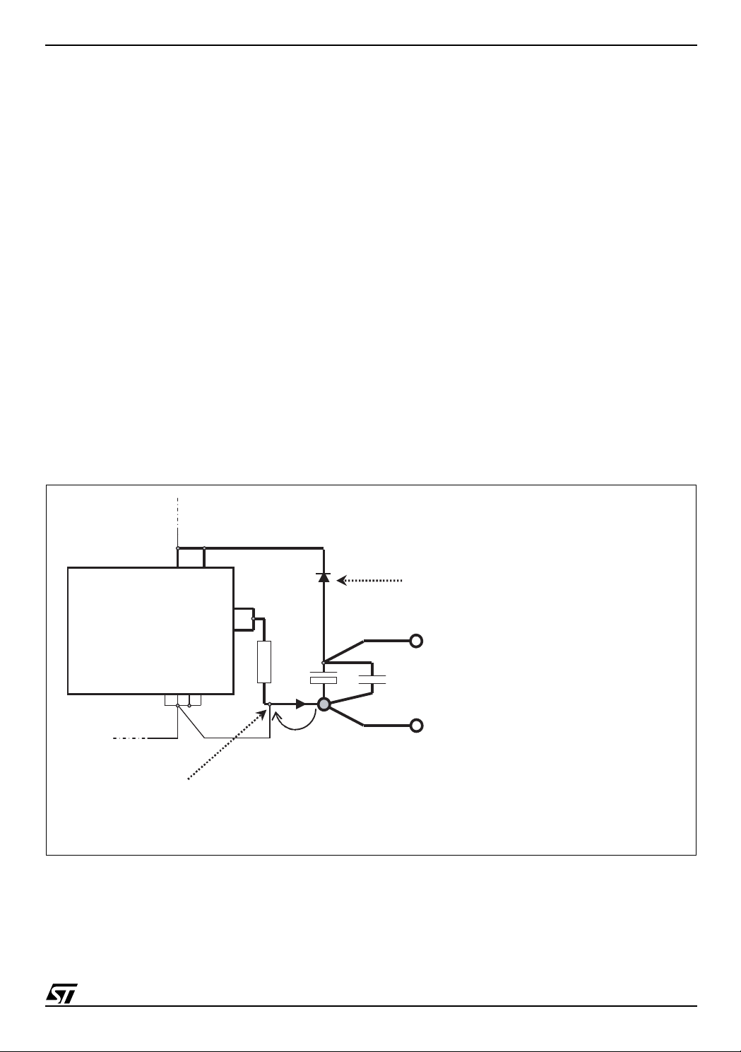
2.4 Layout Considerations
Working with devices that combine high power switches and control logic in the same IC, careful attention has
to be paid to the PCB lay out. In extreme cases, Power DMOS commutation can i nduce nois es that could c ause
improper operation in the logic section of the device. Noise can be radiated by high dv/dt nodes or high di/dt
paths, or conducted through G ND or Supply connectio ns. Logic connec tions, es pecial ly hi gh-i mpedance nodes
(actually all logic inputs, see further), must be kept far from switching nodes and paths. With the L6208, in particular, external components for the charge pump circuitry should be connected together through short paths,
since these components are subjec t to voltage and current swi tching at re lative ly high frequenc y (600kHz ). Primary mean in minimizing conducted noise is working on a good GND layout (see Figure 5).
Figure 5. Typ ic a l App li ca ti on and Layout suggest io ns.
OUT
1B
2-Phase
Stepper Motor
V
BOOT
2B
L6208
C3
R3
D1
C5
R4
RC
B
6/43
+
Logic Supply
3.3 ÷ 5 V
-
µC
or
Custom Logic
V
= 0 ÷1V
ref
OUT
OUT
OUT
1A
2A
CW / CCW
CONTROL
RESET
HALF / F ULL
CLOC
R1
EN
V
refB RCA
V
refA
C1
C2
R2
D2
CP
V
SA VSB
SENSE
SENSE
C8
A
B
R5 R6
C6
+
C7
VS = 8 ÷ 52 V
-
GND GND GND GND
C4
AN1451 APPLICATION NOTE
High current GND tracks (i.e. the tracks connected to the sensing resistors) must be connected directly to the
negative terminal of the bulk capacitor. A good quality, high-frequency bypass capacitor is also required (typically a 100nF÷200nF ceramic would suffice), since electrolytic capacitors show a poor high frequency performance. Both bulk electrolytic and high frequency bypass capacitors have to be connected with short tracks to
V
, VSB and GND. On the L6208 GND pins are the
SA
them. Logic GND and Power GND should be connected together in a
noise in the Power GND from affecting Logic GND. Specific care should be paid layouting the path from the
SENSE
pins through the sensing resistors to the negative terminal of the bulk capacitor (Power Ground). These
tracks must be as s hort as possible in order to mi nimize par asitic inductances that c an cause danger ous voltage
spikes on
the capacitors on V
SENSE
and
OUT
pins (see the
, VSB and GND should be very close to the GND and supply pins. Refer to the Sensing
SA
Voltage Ratings and Operating Range
Resistors section for information on selecting the sense resistors. Traces that connect to V
SENSE
, and the four
B
OUT
pins must be designed with adequate width, since high currents are flowing through
these traces, and l ayer chan ges should be avoided. Should a l ayer ch ange prove necessa ry , multi ple and large
via holes have to be used. A wide GND copper area can be used to improve power dissipation for the device.
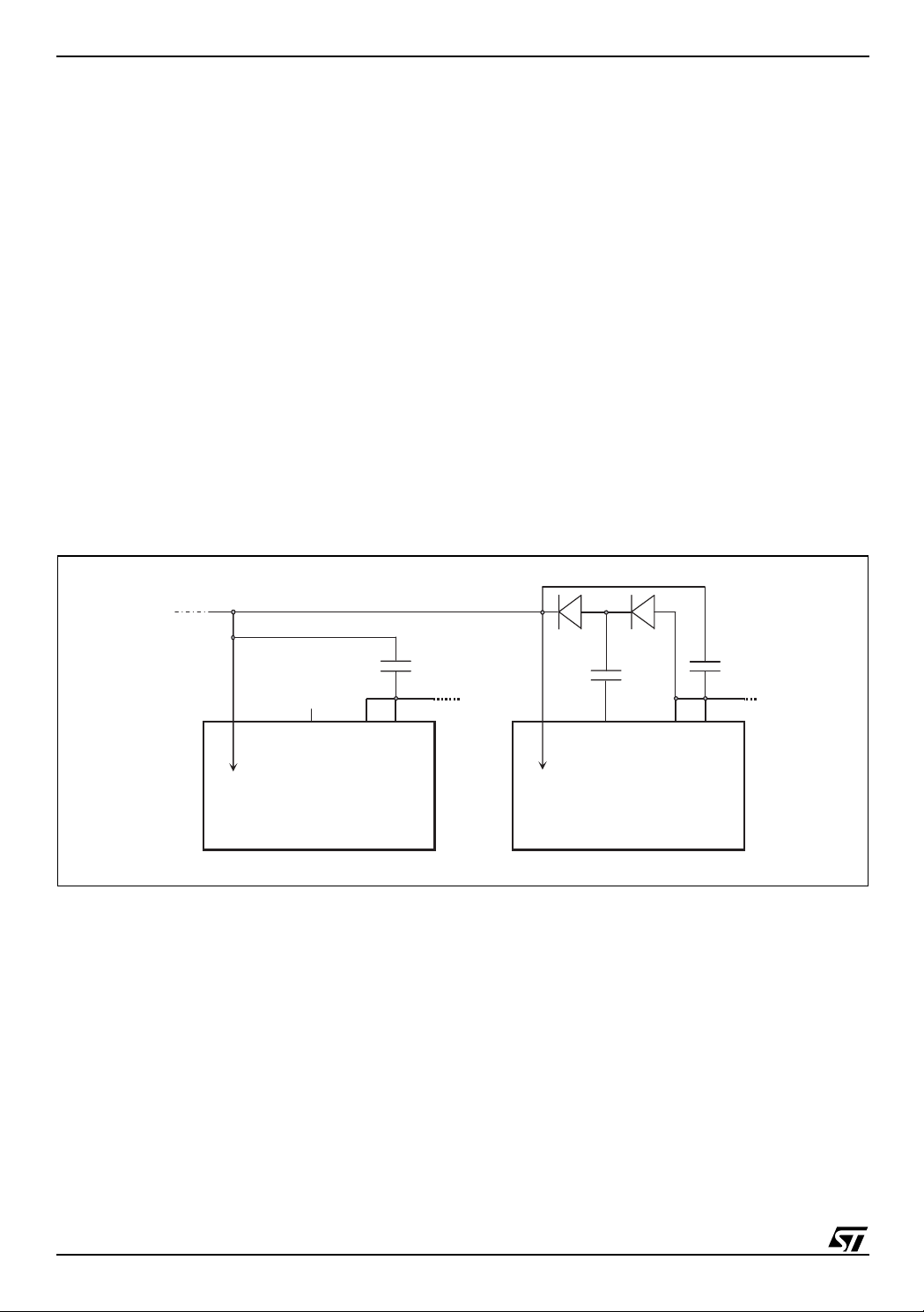
Figure 6 shows two typical situations that must be avoided. An important consideration about the location of the
bulk capacitors is the abi lity to abs orb the inductiv e ener gy from the load, without all owing the s upply v oltage to
exceed the maximum rating. The diode shown in Figure 6 prevents the recirculation current from reaching the
capacitors and will res ult in a high voltage on the IC pins th at can destroy the device. H aving a switch or a power
connection that can dis connect the c apacitors from the IC, w hile there is stil l c ur rent in the motor, will a lso result
in a high voltage transient since there is no capacitance to absorb the recirculation current.
Logic
GND, since only the quiescen t curr ent flows thr ough
single point
, the bulk capacitor, to keep
section); for the same reason
, VSB, SENSEA,
SA
Figure 6. Two situations that must be avoided.
V
SA VSB
SENSE
A
SENSE
B
L6208
GND
GND
GND
GND
R5
C6
DON’T connect the Logic GND here
Voltage drop due to c urrent in sens e
path can disturb lo gic GND.
DON’T put a di ode here!
Recircul at ing current cannot flow into t he
bulk cap ac itor and c aus es a high volt age
spike that c an des troy the IC.
+
C7
VS = 8 ÷ 52 V
-
7/43

AN1451 APPLICATION NOTE
2.5 S en sing Resistors
Each motor winding current is flowing through the corresponding sensing resistor, causing a voltage drop that
is used, by the logic, to control the peak value of the load current. Tw o issues must be taken into account when
choosing the R
– The sensing resistor dissipates energy and provides dangerous negative voltages on the
during the current recirculation. For this reason the resistance of this component should be kept low.
– The voltage drop acros s R
comparator. The lower is the R
and to the input offset of the current sense comparator: too small values of R
A good compromise is calculating the sensi ng resistor value so that the voltage drop , corresponding to the peak
current in the load (I
It should be clear that sensing resistor must absolutely be non-inductive type in order to avoid dangerous negative spikes on
ommended for their high peak current capability and low inductance. For the same reason the connections
between the
(see also the
SENSE
Layout Considerations
The average power dissipated by the sensing resistor is:
value:
SENSE
SENSE
SENSE
), is about 0.5 V: R
peak
SENSE
pins. Wire-wounded resistors c annot be used here, whi le Metall ic film res istor s are rec-
pins, C6, C7, VSA, VSB and
section).
SENSE
is compared with the reference voltage (on V
pin) by the internal
ref
value, the higher is the peak current error due to noise on Vref pin
must be avoided.
SENSE
SENSE
= 0.5 V / I
GND
pins (see Figure 5) must be taken as short as possible
peak
.
pin
Fast Decay Recirculation: P
R
≈ I
Slow Decay Recirculation: PR ≈ I
D is the duty-cycle of the PWM current control, I
rms
rms
· R
2
· R
SENSE
· D,
SEN SE
is the r.m.s. value of the load current.
rms
2
Nevertheless, sensing resistor power rating should be chosen taking into account the peak value of the dissipated power:
where I
is the peak value of the load current.
pk
PRI
pk
2
R
⋅≈
SENSE
,
Using multiple resistors in parallel will help obtaining the required power rating with standard resistors, and reduce the inductance.
R
The following table shows R
tolerance reflects on the peak current error: 1% resistors should be preferred.
SENSE
recommended values (to have 0.5V drop on it) and power ratings for typical
SENSE
examples of current peak values.
I
pk
0.5 1 0.25
1 0.5 0.5 2 X 1Ω, 0.25W paralleled
1.5 0.33 0.75 3 X 1Ω, 0.25W paralleled
2 0.25 1 4 X 1Ω, 0.25W paralleled
R
SENSE
Value
[Ω]
R
SENSE
Power Rating
[W]
Alternatives
8/43
AN1451 APPLICATION NOTE
2.6 Charge pump external components
An internal oscillator, with its output at CP pin, switches from GND to 10V with a typical frequency of 600kHz
(see Figure 7).
Figure 7. Charge Pump .
VS + 10 V - VD1 - V
V
10 V
f = 600 kHz
D2
D1
C5
R4
BOOT CP
To High-Side
Gate Drivers
f = 600 kHz
D2
10 V
V
SA VSB
R
DS(ON)
R
DS(ON)
= 70Ω
= 70Ω
VS + 10 V - VD1
V
C8
- VD1
S
Charge Pump
Oscillator
10 V
5 V
L6208
When the oscillator output is at ground, C5 is charged by VS through D2. When it rises to 10V, D2 is r eve rse
biased and the charge flows from C
imum voltage of V
+ 10V - VD1 - VD2, which supplies the high-side gate drivers.
S
With a differential vol tage betw een V
ical current drawn by the V
R4
Resistor
is added to reduce the maxi mum current i n the exter nal components and to reduce the slew rate of
BOOT
the rising and falling edges of the voltage at the
circuit. For the same reason car e must be taken in realiz ing the PC B layout of
also the
Layout Considerations
D1, D2 : 1N4148
R4 : 100
Ω (1/8 W)
C5 : 10nF 100V ceramic
C8 : 220nF 25V ceramic
Due to the high charge pump frequency, fast diodes are required. Connecting the cold side of the bulk capacitor
(C8) to V
R4 = 100
instead of GND the average current in the external diodes during operation is less than 10 mA (with
S
Ω
); at startup (when VS is provided to the IC) is less than 200 mA while the reverse voltage is about
10 V in all condi tions. 1N4148 diodes withstand about 200 mA DC (1 A peak), and the maximum rever se voltage
is 75 V, so they should fit for the majority of applications.
to C8 through D1, so the V
5
and V
S
of about 9V and both the bridges switching at 50kHz, the typ-
BOOT
pin, after a few cycles, reaches the max-
BOOT
pin is 1.85 mA.
CP
pin, in order to minimize interferences with the rest of the
R4, C5, D1, D2
connections (see
section). Recommended values for the charge pump circuitry are:
9/43
AN1451 APPLICATION NOTE
2.7 S ha ring the Charge Pump Circuitry
If more than one device is used in the applic ation, it's possible to use the char ge pump from one L6208 to suppl y
the V
Figure 8. A 100nF capacitor (C8) should be connected to the V
Supply voltage pins (V
The higher the number of devices sharing the same charge pump, the lower will be the differential volt age avail-
able for gate drive (V
In this case it's recommended to omit the resistor on the
charge pump circuitry.
Better performance can als o be obtained using a 33nF capacitor for C5 and using s chottky diodes (for ex ample
BAT47 are recommended).
Sharing the same charge pump ci rcuitr y fo r mor e than 3÷4 devi ces is not recommended, sinc e it wil l reduce the
V
BOOT
Figure 8. Sharing the charge pum p circuitry.
pins of several ICs. The unused CP pins on the slaved devices are left unconnected, as shown in
BOOT
pin of each device.
BOOT
) of the devices sharing the charge pump must be connected together.
S
- VS), causing a higher R
BOOT
for the high side DMOS, so higher dissipating po wer.
DS(ON)
CP
pin, obtaining a higher current capability of the
voltage increasing the high-side MOS on-resistance and thus power dissipation.
To other Devices
V
BO OT
To High-Side
Gate Drivers
D2 = BAT47
CP
V
SA VSB
C8 = 100nF
L6208
V
BOOT
To High-Side
Gate Drivers
D1 = BAT47
C5 = 33nF
C18 = 100 nF
V
V
SA
CP
SB
L6208
10/43
AN1451 APPLICATION NOTE
2.8 Reference Voltage for PWM Current Control
The device has two analog inputs, V
peak value of the motor curr ent through th e integrated PWM circuitry . In typical applications these p ins ar e connected together, in order to obtain the same current in the two motor windings (one exception is the microstepping operation; see the related section). A fixed reference voltage can be easily obtained through a resistive
divider from an available 5 V voltage rail (maybe the one supplying the µC or the rest of the application) and
GND.
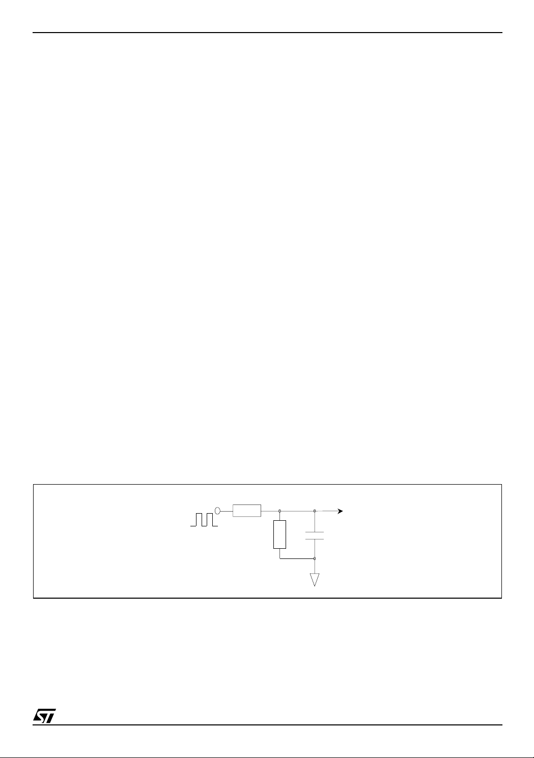
A very simple way to obtain a variable voltage without using a DAC is to low-pass filter a PWM output of a µC
(see Figure 9).
Assuming that the PWM output swings from 0 to 5V, the resulting voltage will be:
refA
and V
V
ref
, connected to the internal sense comparators, to control the
refB
5V DµCR
⋅⋅
-----------------------------------------=
R
LPRDIV
DIV
+
where D
Assuming that the µC output impedance is lower than 1k
is the duty-cycle of the PWM output of the µC.
µC
Ω,
with RLP = 56kΩ, R
= 15kΩ, CLP = 10nF and a
DIV
µC PWM switching fr om 0 to 5V at 100kHz , the l ow pass fi lter tim e consta nt is about 0.12 ms an d the remai ning
ripple on the V
voltage will be about 20 mV. Using higher values for RLP, R
ref
and CLP will reduce the ripple,
DIV
but the reference voltage will tak e more time to vary after changing the duty -cycle of the µC PWM, an d too high
values of R
As sensing resistor values are typically kept small, a small noise on V
will also increase the im pedance of the V
LP
net at low frequencies, causing a poor nois e immunity.
ref
input pins might cause a considerable
ref
error in the output current. It's then recommended to decouple these pins with cerami c capaci tors of some tens
of nF, placed very close to V
and GND pins. Note that V
ref
pins cannot be l eft unconnected, while, if connected
ref
to GND, zero current is not guaranteed due to voltage offset in the sense comparator. The best way to cut down
EN
(IC) power consumption and clear the load current is pulling down the
pin. In slow decay, with very small
reference voltage, PWM integrated circuitry can loose control of the current due to the minimum allowed duration of t
(see the
ON
Programmable off-time Monostable
section).
Figure 9. Obt ain in g a va ri abl e v ol ta ge t hro ugh a PWM ou t put of a µC .
PWM Output
of a µC
R
LP
R
DIV
V
ref
C
LP
GND
11/43

AN1451 APPLICATION NOTE
2.9 Input Logi c pin s
CW/CCW, CONTROL, RESET, HALF/FULL, CLOCK
ator has been realized with hysteresis to ensure the required noise immunity. Typical values for turn-on and turn-off
thresholds are V
= 1.8V and V
th,ON
= 1.3V. Pins are ESD protected (see Figure 10) (2kV human-body electro-
th,OFF
static discharge), and can be direc tly connected to the logic outputs of a µC; a series resistor is generally not reco mmended, as i t c ould help inducted noise to disturb the inputs. All logi c pins enforce a specific behavi or and cannot be
left unconnec ted.
Figure 10. Logic input pins.
are CMOS/TTL compatible lo gic input pins. The input compar-
CONTROL,
HALF/FULL, CLOCK,
RESET, CW/CCW
ESD
Protection
5 V
2.10EN pin
The EN pin is, actually, bi-directional: as an input, with a comparator similar to the other logic input pins (TTL/CMOS
with hyst eresis), it c ontrols the s tate of the PowerDMOS. When th is pin is at a low logic level, all t he PowerDMOS ar e
turned off. The EN pin is als o connected to the open drai n output of the protection circuit that will pull the pin to GND
if over current or over temperature conditions exist. For this reason, EN pin must be driven through a series resistor
of 2.2k
Ω
minimum (for 5V logic), to al lo w the voltage at the pin to be pulled below t he turn-off threshold.
A capaci tor (C1 i n Figu re 5) conne cted be tween t he EN pin and GND is al so re commended , to redu ce the r.m.s . val ue
of the output current when overcurrent conditions persist (see
Over Current Protection
section). EN pin must not be
left unconnec ted.
Figure 11. EN input pin.
5 V
12/43
EN
ESD
Protection

AN1451 APPLICATION NOTE
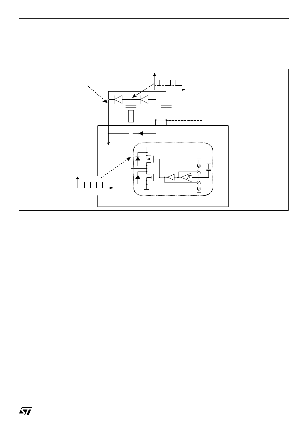
2.11 Programmable off-time Monostable
The L6208 includes a constant off time PWM current controller for each of the two bridges. The current control
circuit senses the bridge current by sensing the voltage drop across an external sense resistor connected between the source of the two lower power MOS transistors and ground, as shown in
the motor builds up the voltage across the sense resistor increases proportionally. When the voltage drop
across the sense resistor becomes greater than the voltage at the reference input (VREF
comparator triggers the monostable switching the bridge off. The power MOS remain off for the time set by the
monostable and the motor current recirculates as defined by the selected decay mode, described in the next
section. When the monostable times out the bridge w ill again turn on. S ince the inter nal dead time, us ed to prevent cross c onduction in the bridge, delays the turn on of the power MOS, the effecti ve off time is the s um of the
monostable time plus the dead time.
Figure 12. PWM Current Controller Simplified Schematic
(or B)
VS
A
TO GATE LOGIC
BLANKING TIME
MONOST ABLE
1µs
FROM THE
LOW-SIDE
GATE DRIVERS
Figure 12
. As the current in
or VREFB) the sense
A
5mA
5V
C
OFF
Figure 13
MONOSTABLE
(0) (1)
RC
R
OFF
A(or B)
2.5V
S
Q
R
-
+
SET
BLANKER
SENSE
COMPARATOR
COMPARATOR
OUTPUT
DRIVERS
+
DEAD TIME
+
-
VREF
shows the typical operating waveforms of the output current, the voltage drop across the sensing re-
2H 1H
2L 1L
A(or B)
R
SENSE
DRIVERS
+
DEAD TIME
SENSE
A(or B)
OUT2
OUT1
I
OUT
A(or B)
A(or B)
D01IN1332
2 PHASE
STEPPER MOTOR
sistor, the RC pin vol tage and the status of the bridge. More d etails regarding the S ynchronous Rectificati on and
the output stage configuration are included in the next section.
Immediately after the Power MOS turns on, a high peak current flows through the sensing resistor due to the
reverse recovery of the freewheeling diodes. The L6208 provides a 1
µ
s Blanking Time t
that inhibits the
BLANK
comparator output so that this current spike cannot prematurely re-trigger the monostable.
13/43

AN1451 APPLICATION NOTE
Figure 13. Output Current Regulation Waveforms
I
OUT
V
REF
R
SENSE
V
SENSE
V
V
2.5V
OFF
REF
0
RC
5V
ON
SYNCHRONOUS OR QUASI
SYNCHRONOUS RECTIFICATION
D01IN1334
t
OFF
1µs t
BLANK
t
ON
t
1µs t
Slow Decay Slow Decay
Fast Decay
t
RCRISE
t
RCFALL
1µs t
DT
BC
DDA
Fast Decay
t
RCRISE
t
RCFALL
1µs t
BC
OFF
BLANK
DT
Figure 14
shows the magnitude of the Off Time t
OFF
culated from the equations:
t
t
where R
20K
0.47nF ≤ C
t
= 0.6 · R
RCFALL
= t
OFF
RCFALL
and C
OFF
Ω ≤
R
= 1µs (typical value)
DT
OFF
+ tDT = 0.6 · R
are the external component values and tDT is the internally generated Dead Time with:
OFF
≤ 100K
OFF
≤ 100nF
OFF
· C
Ω
OFF
OFF
· C
OFF
+ t
Therefore:
t
OFF(MIN)
t
OFF(MAX)
These values allow a sufficient range of t
The capacitor value chosen for C
The Rise Time t
= 6.6µs
= 6ms
RCRISE
to implement the drive circuit for most motors.
OFF
also affects the Rise Time t
OFF
will only be an issue if the capacitor is not completely charged before the next time the
monostable is triggered. Therefore, the on time t
be bigger than t
14/43
for allowing a good current regulation by the PWM stage. Furthermore, the on time t
RCRISE
versus C
DT
, which depends by motors and supply parameters, has to
ON
OFF
and R
RCRISE
values. It can be approximately cal-
OFF
of the voltage at the pin RCA (or RCB).
ON

AN1451 APPLICATION NOTE
can not be smaller than the minimum on time t
t
>1.5µs (typ. value)=
ONtON MIN()
t
ONtRCRISEtDT
RCRISE
= 600 · C
t
–>
OFF
ON(MIN)
.
2.11.1 Off-time Selection and minimum on-time
Figure 14
has to be said that t
smaller than t
also shows the lower limit for the on time tON for having a good PWM current regulation capacity. It
is always bigger than t
ON
- tDT. In this last case the device continues to work but the off time t
RCRISE
ON(MIN)
because the device imposes this condition, but it can be
stant.
So, small C
switching frequency), but, the smaller is the value for C
value gives more flexibility for the applications (allows smaller on time and, therefore, higher
OFF
OFF
performance.
Figure 14. Off-time selection and minimum on-time.
4
1.10
3
1.10
is not more con-
OFF
, the more influential will be the noises on the circuit
R = 100 kΩ
R = 47 kΩ
R = 20 kΩ
10 0
to f f [ us]
10
1
0.1 1 10 10 0
Coff [nF]
100
10
to n ( m in ) [ u s]
1
0.1 1 10 100
Coff [nF]
15/43

AN1451 APPLICATION NOTE
2.11.2 Decay Modes
The CONTROL input is used to select the behavior of the bridge during the off time. When the CONTROL pin
is low, the Fast Decay mode is selected and both transistors in the bridge are switched off during the off time.
When the CONTROL pin is high, th e S low De cay mode i s s elected and onl y th e low s ide trans istor of the bridge
is switched off during the off time.
Figure 15
MOS are switched off and the current recirculates through the two opposite free wheeling diodes. The current
decays with a high di/dt since the voltage acr oss the coi l is essenti ally the power supply vol tage. After the dead
time, the lower power MOS in paralle l wi th the conduc ting diod e is turned on in synchronous recti fication mode.
In applications where the m otor curr ent is low it is possi ble that the cur rent can decay com pletely to zer o during
the off time. At this poi nt i f both of the power M OS w ere oper ating in the sync hronous rec tificati on mode it would
then be possible for the current to build in the opposite direction. To prevent this only the lower power MOS is
operated in synchronous rectification mode. This operation is called Quasi-Synchronous Rectification Mode.
When the monostable times out, the power MOS are turned on again after some delay set by the dead time to
prevent cross conduction.
Figure 16
MOS is switched off and the current recirculates around the upper half of the bridge. Since the voltage across
the coil is low, the current decays slowly. After the dead time the upper power MOS is operated in the synchronous rectification mode. When the monostable times out, the lower power MOS is turned on again after some
delay set by the dead time to prevent cross conduction.
Figure 15. Fast Decay Mode Output Stage Configurations
shows the operati on of the bridge i n the Fast Decay mode. At the start o f the off time, both of the power
shows the operation of the bridge in the Slow Decay mode. At the start of the off time, the lower power
A) ON TIME B) 1µs DEAD TIME C) QUASI-SYNCHRONOUS
D01IN1335
RECTIFICATION
Figure 16. Slow Decay Mode Output Stage Configurations
A) ON TIME B) 1µs DEAD TIME C) SYNCHRONOUS
D01IN1336
16/43
RECTIFICATION
D) 1µs SLOW DECAY
D) 1µs DEAD TIME
AN1451 APPLICATION NOTE
minimu m t
In some conditions (short off-time, very low regulated current, high motor winding L / R) the system may need
an on-time shorter than 1.5µs. In these cases the PWM current controller can loose the regulation.
Figure 17 shows the operation of the circuit in this condition. When the current first reaches the threshold, the
bridge is turned off for a fixed tim e and the current decays. During the foll owing on-time current incr eases above
the threshold, but the bridge cannot be turned off until the minimum 1.5µs on-time expires. Since current increases more in each on-time than it decays during the off-time, it keeps growing during each cy cle, with steady
state asymptotic value set by duty-cycle and load DC resistance: the resulting peak current will be
I
= VS · D / R
pk
LOAD
,
where D = t
/ (tON + t
ON
) is the duty-cycle and R
OFF
is the load DC resistance.
LOAD
Figure 17. Minimum on-time can cause the PWM controller to loose the regulation.
is about 1.5 µs
needed tON is
than 1.5 µs
ON
less
V
/ R
ref
SENSE
17/43
AN1451 APPLICATION NOTE
2.12 Over Current Protection
To implement an O ver Cur rent (i.e. shor t ci rcuit) Pr otection, a dedi cated Over Cur rent D etection (OCD) circ uitry
(see Figure 18 for a simplified schem atic) senses the current in each high side. P ower DMOS are actually made
up with thousands of individual identical cells, each carrying a fraction of the total current flowing. The current
sensing element, connected in parallel to the Power DMOS, is made only with few such cells, having a 1:N ratio
compared to the power DMOS. The total drain current is split between the output and the sense element according to the cell ratio. Sensed current is, then, a small fraction of the output current and will not contribute
significantly to power dissipation.
Figure 18. Over Current Detection simplified circuitry.
OUT
1A
I
I
/ n
1A
(I1A+I2A) / n
I
V
SA
1A I2A
+
REF
2A
POWER DMOS
n cells
I
/ n
2A
HIGH SIDE DMOSs OF
THE BRIDGE A
POWER SENSE
1 cell
µC or LOGIC
+5V
R
.EN
EN
C
.
EN
TO GATE
R
DS(ON)
60Ω TYP.
LOGIC
INTERNAL
OPEN-DRAIN
POWER SENSE
1 cell
OCD
COMPARATOR
OUT
POWER DMOS
n cells
OVER TEMPERATURE
FROM THE
OCD
COMPARATOR
BRIDGE B
D01IN1337
This sensed current is compared to an internally generated reference to detect an over current condition. An
internal open drain mosfet tur ns on when the sum of the currents in the bridges 1A and 2A or 1B and 2B reac hes
the threshold (5.6A typical value); the open drain is internally connected to the
EN
pin. To ensure an over current
protection, connect this pin to an external RC network (see Figure 18).
Figure 19 shows the device operating in overcurrent condition (short to ground). When an over current is de-
tected the internal open drai n mosfet pulls the
EN
pin to GND switchi ng off all 8 power DMOS of the device and
allowing the cur rent to decay . Under a persistent over current c ondition, lik e a short to ground or a shor t between
two output pins, the external RC network on the
current by imposing a fixed disable-time after each over current occurrence. The values of
EN
pin (see Figure 18) reduces the r.m.s. value of the output
R
and
EN
C
EN
are
selected to ensure proper operation of the device under a short circuit condition. When the current flowing
through the high side DMOS reaches the OCD threshold (5.6 A typ.), after an internal propagation delay
(t
OCD(ON)
(V
decay as it circulates through the freewheeling diodes. Since the DMOS are
through them and no current to sense so the OCD circuit, after a short delay (t
open drain device off, and
(V
rent can be very high, the external RC network provides a disable time (t
) the open drain starts discharging
TH(OFF)
) all the Power DMOS turn off after the internal propagation delay (t
R
TH(ON)
), after the t
D(ON)EN
delay, the DMOS turn on and the current restarts. E ven if the max imum ou tput cur-
can charge
EN
C
. When the EN pin voltage falls below the turn-off threshold
EN
D(OFF)EN
OCD(OFF)
C
. When the voltage at EN pin reaches the turn-on threshold
EN
DISABLE
). The current begins to
off
, there is no current flowing
), switches the internal
) to ensure a safe r.m.s. value
(see Figure 19).
18/43

Figure 19. Over Current Operation.
t
DELAY
t
OCD(ON)
Outp ut Current
I
S OVER
t
EN(FALL)
t
D(OFF)EN
AN1451 APPLICATION NOTE
t
DISABLE
Ou tput Curr ent
t
D(ON)EN
V
TH(OFF)
t
OCD(OFF)
t
DISABLE
EN
V
V
TH(ON)
EN(LOW)
t
EN(RISE)
EN
The maximum value reached by the current depends on its slew-rate, so on the short circuit nature and supply
voltage, and on the total intervention delay (t
imum value reached by the output cur rent beco mes l ower, bec ause the capacitor on
ing from a lower voltage, resulting in a shorter t
). It can be noticed that after the first current peak, the max-
DELAY
EN
pin is disch arged star t-
.
DELAY
The following approximate relations estimate the disable time and the first OCD intervention delay after the short
circuit (worst case).
The time the device remains disabled is:
t
DISABLE
= t
OCD(OFF)
+ t
EN(RISE)
+ t
D(ON)EN
where
V
–
DDVEN LOW()
-------------------------------------------- -
EN
ln⋅⋅=
–
V
DDVTH ON()
V
EN(LOW)
t
EN RISE()
RENC
is the minimum voltage reached by the EN pin, and can be estimated with the relation:
The total intervention time is
where
t
OCD(OFF)
, t
OCD(ON)
, t
D(ON)EN
V
EN LOW()
t
DELAY
t
EN FALL()
, t
D(OFF)EN
= t
OCD(ON)
, and R
t
DOFF()ENtOCD OFF()
-------- ------------- -------------- ---------- ------------- -
V
TH OFF()
R
OPDRCEN
OPDR
e
⋅=
+ t
EN(FALL)
are device intrinsic parameters, VDD is the pull-up voltage
+
R
⋅
OPDRCEN
+ t
D(OFF)EN
V
-------------------------
ln⋅⋅=
V
TH OFF()
DD
19/43

AN1451 APPLICATION NOTE
applied to REN.
The external RC network, C
) and a safe disable ti me (long t
t
DELAY
at least 100µs for t
DISABLE
The internal open drain can also be turned on if the device experiences an
The OVT will cause the device to shut down when the die temperature exceeds the OVT threshold
(T
>165 °C typ.). Since the OVT is also connected directly to the gate drive circuit (see Figure 1), all the Power
J
DMOS will shut down, even if
OVT turn-off threshold (150 °C typ.), the open drain turns off,
erDMOS are turned on back.
Figure 20. Typical disable and delay time as a function of CEN, for several values of REN.
in particular, must be chosen obtaining a reasonable fast OCD intervention (short
EN
DISABLE
). Figure 20 shows both t
DISABLE
and t
as a function of CEN:
DELAY
are recommended, keeping the delay time below 1÷2µs at the same time.
EN
pin voltage i s still over V
over temperature
. When the junction temperatur e fall s b elow the
th(OFF)
C
is recharged up to V
EN
TH(ON )
(OVT) condition.
and then the Pow-
1.10
3
100
REN = 220 kΩ REN = 100 kΩ
R
= 47 kΩ
EN
R
= 33 kΩ
EN
= 10 kΩ
R
EN
[µs]
DISABLE
t
10
1
110100
CEN [nF]
10
[µs]
1
DELAY
t
20/43
0.1
110100
CEN [nF]

AN1451 APPLICATION NOTE
2.13 Power Management
Even when operating at current l evels well below the maxi mum ratings of the devi ce, the operating juncti on temperature must be kept below 125 °C.
Figure 21 shows the IC dis sipated power versus the r.m.s. load curr ent, in 4 different dri ving sequences, as suming the supply voltage is 24V.
Figure 21. IC Dissipated Power versus Output Current.
PD [W]
PD [W]
PD [W]
10
8
6
4
2
0
HALF STEP
0 0.5 1 1.5 2 2.5 3
I
[A ]
OUT
NORMAL DRIVE
10
8
6
4
2
0
00.511.522.53
I
[A]
OUT
WAVE DRIVE
10
8
6
4
2
0
0 0.5 1 1.5 2 2.5 3
I
[A]
OUT
MICROSTEPPING
10
I
A
I
B
I
OUT
I
OUT
Test Conditions:
Supply Voltage = 24V
No PWM
f
= 30 kHz ( slow decay)
SW
I
A
I
B
I
A
I
B
I
A
I
OUT
I
OUT
Test Conditions:
Supply Voltage = 24 V
No PWM
= 30 kHz (slow decay)
f
SW
I
OUT
I
OUT
Test Conditions:
Supply Voltage = 24V
No PWM
f
= 30 kHz (slow decay)
SW
I
OUT
PD [W]
8
6
4
2
0
0 0.5 1 1.5 2 2.5 3
[A]
I
OUT
I
B
Test Conditions:
Supply Voltage = 24V
fSW = 30 k
fSW = 50 k
I
OUT
Hz (slow decay)
Hz (slow decay)
21/43

AN1451 APPLICATION NOTE
2.13.1 Maximum output current vs. selectable devices
Figure 22 reports a performance comparison between L6228 (std. power) and L6208 (high power) for different
packages, with the following assumptions:
- Normal Drive Mode (two-phase on)
- Supply voltage: 24 V; Switching frequency: 30 kHz.
= 25 °C, TJ = 125 °C.
- T
amb
- Maximum R
- Maximum quiescent current I
- PCB is a FR4
SO and PowerDIP packages (D, N suffixes).
- PCB is a FR4
via holes and a ground layer for the PowerSO package (PD suffix).
- For each device (on the x axis) y axis reports the maximum output current.
Figure 22. Maximum output current vs. selectable devi ces.
(taking into account process spread) has been considered, @ 125 °C.
DS(ON)
(taking into account process spread) has been considered.
Q
with a dissipating copper surface on the top side of 6 cm2 (with a thickness of 35 µm) for
with a dissipating copper surface on the top side of 6 cm2 (with a thickness of 35 µm ), 16
1.70
1.50
1.30
1.10
Load Current
[A]
0.90
0.70
0.50
D
8
2
2
6
L
2.13.2 Power Dissipation Formulae for different sequences
Figure 23 to Figure 26 are screenshots of a spreadsheet that helps calculating power dissipation in specified
conditions (application and motor data), and estimates the resulting junction temperature for a given package
and copper area available on the PCB [6]. The model considers power dissipation during the on-time and the
off-time, taking into account the selected decay, rise and fall time (when a phase change occurs) considering
the operating sequence, the switching losses and the quiescent current power dissipation.
N
8
2
2
6
L
PD
8
2
2
6
L
D
8
0
2
6
L
N
8
0
2
6
L
PD
8
0
2
6
L
22/43

AN1451 APPLICATION NOTE
"SLOW " = Synch ronous Slow D ecay
"FAST" = Qu asi-Synchronous Fast decay
s
Figure 23. Definition of parameters for the three different sequences. The current in only one phase
is shown.
NORMAL
I
I
pk
T
r
Figure 24. Input Data.
WAVE
T
∆∆∆∆I
I
load
t
T
load
T
f
I
T/2
∆∆∆∆I
I
I
pk
load
t
T
r
T
load
T
f
HALF STEP
I
I
pk
T
r
T
∆∆∆∆I
I
load
t
T
load
T
f
Input D ata
Device Input Values
Maximum D rain-Source ON R esistance Ron = 5.60E-01 [Ohm] Average Value between H igh-Side and Low-Side
Maximum diode voltage Vd = 1.20E+00 [V]
Quiescent Current Iq = 5.50E-03 [mA]
Motor Input Value
Maximum BEMF Voltage Vb = 1.50E+01 [V]
Mo to r In ductanc e Lm = 7.90E - 0 3 [H]
Motor Resistance Rm = 6.60E+00 [Ohm]
Application Input Values
Supply Voltage Vs = 2.40E+01 [V]
Peak Current Ipk = 1.00E+00 [A]
Off-Time tOFF = 1.50E-05 [s]
Step Frequency fCK = 1.00E+03 [Hz]
Sensing Resistance Rs = 5.00E-01 [Ohm]
Decay Type -
Stepping sequence - "NORM A L", "HALF" or "WA VE "
SLOW
WAVE
23/43
AN1451 APPLICATION NOTE
Figure 25. Power Dissipation formulae and results.
Result
PowerDMOS
Commutation
Time
Tcom =
9.60E-08 [s] Vs / (250V/µs)
Rise Ti m e Trise =
Fall Time Tfall =
4.03E-04 [s]
3.16E-04 [s]
Duty Cycle D = 6.25E-01 -
Switching
Frequency
Current Ripple
Period T =
Load Time
Tload =
2.50E+04
fSW =
∆I = 2.85E-02 [A] (Vs - Vb)*D / (Lm* fSW)
2.00E-03 [s]
5.97E-04 [s]
Average Cur-
rent during
I =
9.86E-01 [A]
Load Time
r.m.s. Current
during Load
Irms =
9.86E-01 [A]
Time
Rise Tim e
Dissipating
Erise =
1.50E-04 [J]
Energy
[Hz]
Ipk Rm 2 Ipk Ron Ipk Rs Vs+⋅–⋅⋅–⋅–()
---------------------------------------------------------------------------------------------------------------
-------------------------------------------------------------------------------------------------------------
Ipk Rm 2+ Ipk Ron Ipk Rs Vs+⋅+⋅⋅⋅()
-------------------------------------------------------------------------------------------
Ipk Rm Ipk Rs Vs 2 Vd⋅–+⋅+⋅()
Vs
Vs
Vs 2 Vd⋅–()
-------------------------------------------------------
⋅ln–
Vb / Vs
(Vs + Vb) / 2Vs
Lm
--------------------------------------------- -
⋅ln–
Rm Rs 2Ron++
Lm
NORMAL Mode
Rm 2 Ron Rs+⋅+()
Lm
----------------------------
⋅ln–
Rm Rs+()
HALF or WAVE
Mode
Sync. Slow Decay
Quasi-Sync F ast Decay
(1-D) / tOF F
2 / fCK
4 / fCK
2 / fCK
T-Trise-Tfall
(3/4)T-rise
(T/2)-Trise
I∆
Ipk
-----–
2
I
2
2
Trise
---------------
3
Tfall
-------------
3
∆
-------+⋅
3
Ipk Ipk I∆–()
2Ron Ipk
⋅⋅
2Ron Ipk
⋅⋅
2
NORMAL Mode
HALF Mode
WAVE Mode
NORMAL Mode
HALF Mode
WAVE Mode
MORMAL Mode
Fall Time
Dissipating
Energy
Load Time
Diss. Energy
Commutatiion
Time
Dissipating Pw
Quiescent
Dissipating Pw
Tot al Di ssi-
pating Power
24/43
Efall =
Eload =
Ecom =
Pq = 1.32E-01
P =
Vs– 2Vd⋅+()
--------------------------------------
Rm Rs+()
3.62E-04 [J]
2VdTfall
1
---------------------------------------------------------------------------------
2
· Tlo a d
6.50E-05 [J]
Lm Ipk Rm Ipk Rs Vs 2 Vd⋅–+⋅+⋅()
⋅⋅
2Ron · Irms
· D ·Tload + (Ron · Irms2 + Vd · I) · (1 - D) · Tload
2Ron · Irms
2
6.78E-05 [J] 2Vs · I · Tcom · Tload · fSW
1.36E+00
[W]
[W]
2
---
·(Erise + Efall + Elo ad + E co m ) + P q
T
Vs · Iq
+⋅⋅
T–fall
----------------
Rm Rs+()⋅exp–
Lm
Rm Rs+()
2
HALF or WAVE
Mode
Sync. Slow Decay
Quasi-Sync F ast Decay

Figure 26. Thermal Data inputs and results.
g
SO2
g
14.00
g
103.60
AN1451 APPLICATION NOTE
Input Data
Packa
Copper Area 4.0 1÷10 sq. cm
Copper Area is on Same side of the device
Ground Layer N/A
Ambient Tem perature 50 -25 ÷ 100 ºC
Thermal Resistance
Junction to Ambient
Thermal Resistance
Junction to Pins / Slu
Estim ated Jun ction
Temperature
Estim ated
Pins / Slu
e
Temperature
4
Results
53.36 ºC / W
ºC / W
122.66 ºC
2.14 Choosing the Decay Mode
L6208 can operate in either fast or slow decay mode, each having a specific recirculation path for the current
during off-time. In slow decay mode only the lower DMOS is turned off and the current recirculates around the
upper half of the bridge so that voltage across the coil is essentially 0. In Fast decay mode both DMOS are
turned off and the current recirculates back to the power suppl y rai l so that voltage acros s the coil is essentiall y
power supply voltage itself.
Slow decay operation provides several advantages: for a given peak current and off-time, current ripple is minimized, and the same is true for acoustic noise and losses in the motor iron (achieving the same current ripple
with fast decay mode w ould require a s horter off-time resu lting in a hi gher switching frequency and higher power
dissipation in the IC). As current recircul ates in the upper half of the bridge and both the high side DMOS in the
same bridge are on,
Also, as no output pin goes below GND (see
is dissipated on the sense resistor during the off-time (see
synchronous
rectification is realized, minimizing power dissipation in the power switches.
Supply Voltage Ratings and Operating Range
Sensing Resistors
section).
section), no power
On the other hand, slow decay can be undesirable in some situations, for example when current has to be regulated at very low values or motor winding L / R ratio is high. In these cases an on-time shorter than the minimum
t
(about 1.5µs) may be requested to r egulate the c urrent, and this c an cause the PWM c ontroller to loos e the
ON
regulation (refer to the
Programmable off-time Monostable
section).
Another situation where fast decay is to be preferred to slow decay is with regulated current expected to vary
over time with a given profile (enforced providing a variable voltage on the V
pins, see also
ref
Microstepping
section). Here fast decay helps following fast decreasing edges in the desired profile.
25/43
AN1451 APPLICATION NOTE
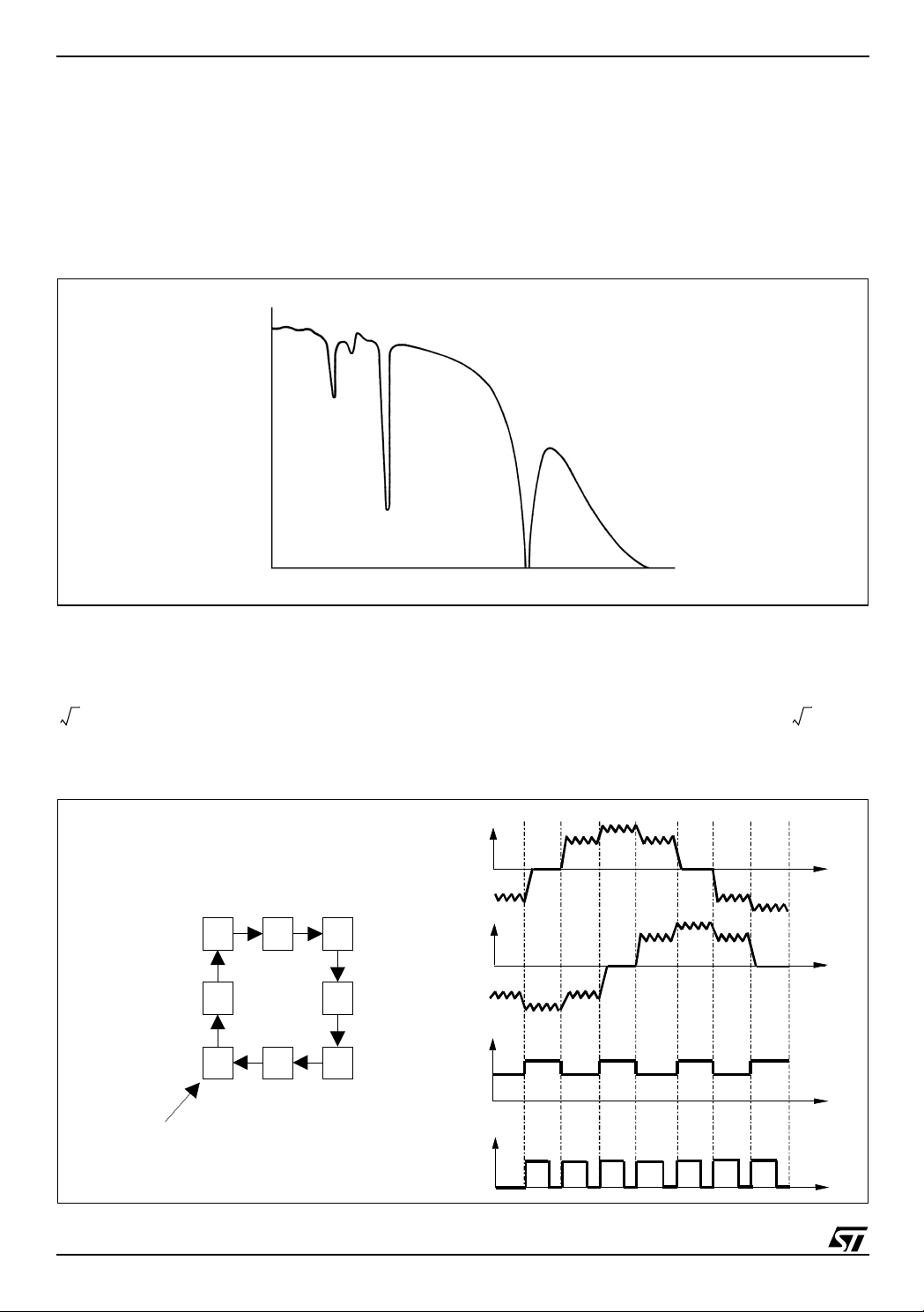
2.15 Choosing the Stepping Sequence
The device can provid e three differ ent s equences to run a s tepper motor : full step two phase on (Normal drive),
full step one phase on (Wave drive) and Half step.
Half S t ep
If
resolution and reducing instability due to low-torque regions in certain motors' speed-torque diagrams, when
used in full step mode (see Figure 27).
Figure 27. Torque instability in full step mode.
driving is used, the motor advances by half a step after each clock pulse, obtaining a higher position
Torque
Speed
Using this driving method the torque is affected by ripple, because in odd-numbered states, when both coils are
driven, the total current in the motor windings is double than in even-numbered states.
A way to avoid the high torque ripple in half step mode is to supply to the motor a higher current (by a factor of
) during the even numbered states , in w hich only one winding is ener gized, s imply by apply ing a higher
2 2
reference voltage at the V
refA
, V
pins during these states (see Figure 28) [2].
refB
Figure 28. Bal anced Half Step f or lo w torque ripple.
I
A
Balanced Half Step
I
V
ref A=Vref B
Clock
B
V
*√√√√2
ref
V
ref
71
823456
Startup or
Reset
3 4 5
2
1
6
78
26/43

AN1451 APPLICATION NOTE
A simple circui t to generate two different r eference voltag es is show n in Figure 29. R1 and R2 should be chosen
to have
R
2
--------------------
⋅==
R1R
+
R
2
R
+()⋅
1
2
2
and R
should be
3
V
ref HIGH,
R
V
ref
--------------------------------------------------- -=
3
21–()R
2⋅ 5V
R
⋅
1
A similar circu it can also be used t o modify the ref erence vol tage in othe r situa tions. For example it' s possible, at constant rotation speed, to reduce the motor torque, and to increase it during acceleration and deceleration. Adding a
second tran si stor is possible to impl em ent 4 different referen ce voltages, selectable by two logic si gnal s.
Figure 29. Realizing Half Step current shaping.
+5V
to V
pin(s)
ref
R
R
1
2
GND
R
3
15k
4.7k
Ω
5V during
odd numbered states
Ω
0V during
even numbered states
Normal and Wave Drive are fullstep modes. In Wave Drive mode the two motor windings are alternately energized, while in Normal Drive both the windings are energized in each state, increasing the torque by a factor of
. On the other hand the total current in the motor is double, so the efficiency is similar. In wave drive mode
2
the torque ripple is higher than in normal drive mode.
2.16 Microstepping
Microstepping operation gives several advantages, including the absence of instability phenomena due to lowtorque regions in certa in motors' speed- torque diagrams (see Figur e 27), reduction of mechanic al nois e and increased position resolution. The L6208 can be used as two-phase microstepping driver IC [5]. The controller
circuitry allows for an easy and inexpensive design with such device. By controlling the V
input it is possible
ref
to get in the two phases variable output currents with a sine-wave shape. A variable voltage proportional to the
desired output current is appl ied to each r eference pin. For micr ostepping, the two inputs are rectifie d sine-wave
voltages with a phase delay of 90°. The L6208 is operated in the normal drive mode and the frequency of the
two sine-wave voltages must be 1/4 of the CLOCK frequency. Figure 30 shows a circuit to generate the two
sine-wave signals us ing low-pass filters and two PWM outputs of a µC (see
Control
section). Figure 31 shows the V
voltages, the CLOCK signal and the output currents.
ref
Reference Voltage for P WM Current
27/43
AN1451 APPLICATION NOTE
Figure 30. Microstepping Application.
PWM
A
56kΩ
15kΩ
10nF
V
refA
5.6nF
V
refB
EN
CONTROL
CW/CCW
CLOCK
RESET
HA LF/FUL L
µC
PWM
OUT
OUT
OUT
OUT
OUT
B
56kΩ
15kΩ
1
100kΩ
2
3
4
5
10nF
L6208
Figure 31. Microstepping reference voltages, output currents and CLOCK signal.
°
I
* R
MAX
SENSE
0 V
.
I
* R
MAX
SENSE
90
V
refA
V
refB
-I
0 V
I
MAX
I
-I
MAX
MAX
MAX
.
I
OUTA
.
I
OUTB
.
5 V
.
0 V
Especially at hi gh rotation speeds, s low decay mode can be inadequate si nce it does not allow the motor current
to decay fast enough, following the decr easing slope of the desired sine wave. In this c ase it' s poss ible to appl y
the fast decay mode just during the negative slope of the current (see Figure 32). The disadvantage is an increased current ripple in the other winding (where the current is increasing and fast decay in not needed).
28/43

Figure 32. Using Fast decay during high negative current slope.
V
refA
V
refB
I
outA
I
outB
5V
CONTROL
AN1451 APPLICATION NOTE
Slow Decay Select ed
CLOCK
0V
Fast Decay Sele cte d
29/43

AN1451 APPLICATION NOTE
3 APPLICATION EXAMPLE
Application Data Motor Data
Rotation Speed: 300 rpm (fCK= 1kHz) Winding Resistance: 6.6
Winding peak Current: 1A Winding Inductance: 7.9mH
Maximum Ripple: 50mA Step Angle: 1.8°/step
Supply Voltage: 24V ±5% Maximum BEMF at 300rpm: 15V
Sequence: Wave Mode
3.1 Decay mode, sensing resistors and refere nce vol tage.
The first step is choosing the decay type. Let's suppose to implement slow decay, which allows lower power
dissipation, lower ri pple and avoids voltag es below GND at output pins during r ecirculation. Refer ring to approximated formulae in Figure 25, it's possible to calculate the Duty-Cycle (D), the Switching Frequency (f
Current Ripple (
D
≅
63%, fSW ≅ 25kHz, ∆I ≅ 29mA. The on-time is tON = D / fSW ≅ 25µs, which is far from the minimum allowed
∆
I). With a 15 µs off-time, we will have:
(1.5µs), so slow decay can be used.
≅
The bulk capacitor need to withstand at least 24V + 5% + 25%
32V. A 50V capacitor will be used. Allowing a
voltage ripple of 200mV, the capacitor ESR should be lower than 200mV / 1A = 200m
bility should be about 1A.
Ω
Providing a reference voltage of 0.5V, 0.5
er rating is about P
R
≅ I
rms
2
· R
SENSE
sensing resistor are needed. In slow decay mode the r esistors pow-
· D ≅ 0.32W. Two 1Ω - 0.25W - 1% resistors in parallel are used. The
charge pump uses recommended components (1N4148 diodes, ceramic capacitors and a 100
duce EMI).
R = 18k
placed, and the pin is driven by the µC through a 100k
Ω
, C = 1.2 nF are connected to the RC pins, obtaining t
Ω
resistor. With these values, in case of short circuit be-
≅ 16µs. On the EN pin a 5.6nF has been
OFF
tween two OUT pins or an OU T pin and GND, the PowerDMOS turns off after about 1µs, and t
Ω
Ω
; the AC current capa-
Ω
DISABLE
), the
SW
resistor to re-
≅ 240µs.
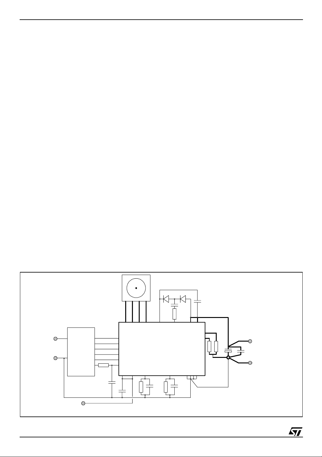
Figure 33. Application Example .
2-Phase
Stepper Motor
V
GND GND GND GND
SA VSB
SENSE
SENSE
220nF 25V
Ceramic
A
B
1 Ω, 0.25 W,
100µF 50V
ESR<200mΩ
+
100nF 50V
Ceramic
4 X
1%
VS = 24 V
-
+
Logic Supply
5 V
-
18 kΩ
0.25 W 1%
2 kΩ
0.25 W 1%
Custo m Lo gic
µC
V
or
= 0.5 V
ref
100 kΩ
5.6 nF
Ceramic
1N4148 1N4148
10nF 50V
100Ω
Ceramic
0.25W
V
OUT
1A
47nF
OUT
2A
V
refB RCA
18 kΩ
5%
OUT
1B
2B
L6208
1.2 nF
Ceramic
OUT
CONTROL
CW / CCW
CLOCK
RESET
HALF / FULL
EN
V
refA
Ceramic
BOOT
18 kΩ
5%
CP
RC
B
1.2 nF
Ceramic
With Wave Drive selected, referring to Figure 24, Figure 25, Figure 26, the dissipating power is about 1.36 W.
If the ambient temperature is lower than 50°C, with 4cm
2
of copper area on the PCB and a SO24 package, the
estimated junction temperature is about 123° C. Using more copper area or a Po werDIP package will reduce the
junction temperature.
30/43
AN1451 APPLICATION NOTE
4 APPENDIX - EVALUATION BOARDS
4.1 PractiSPIN
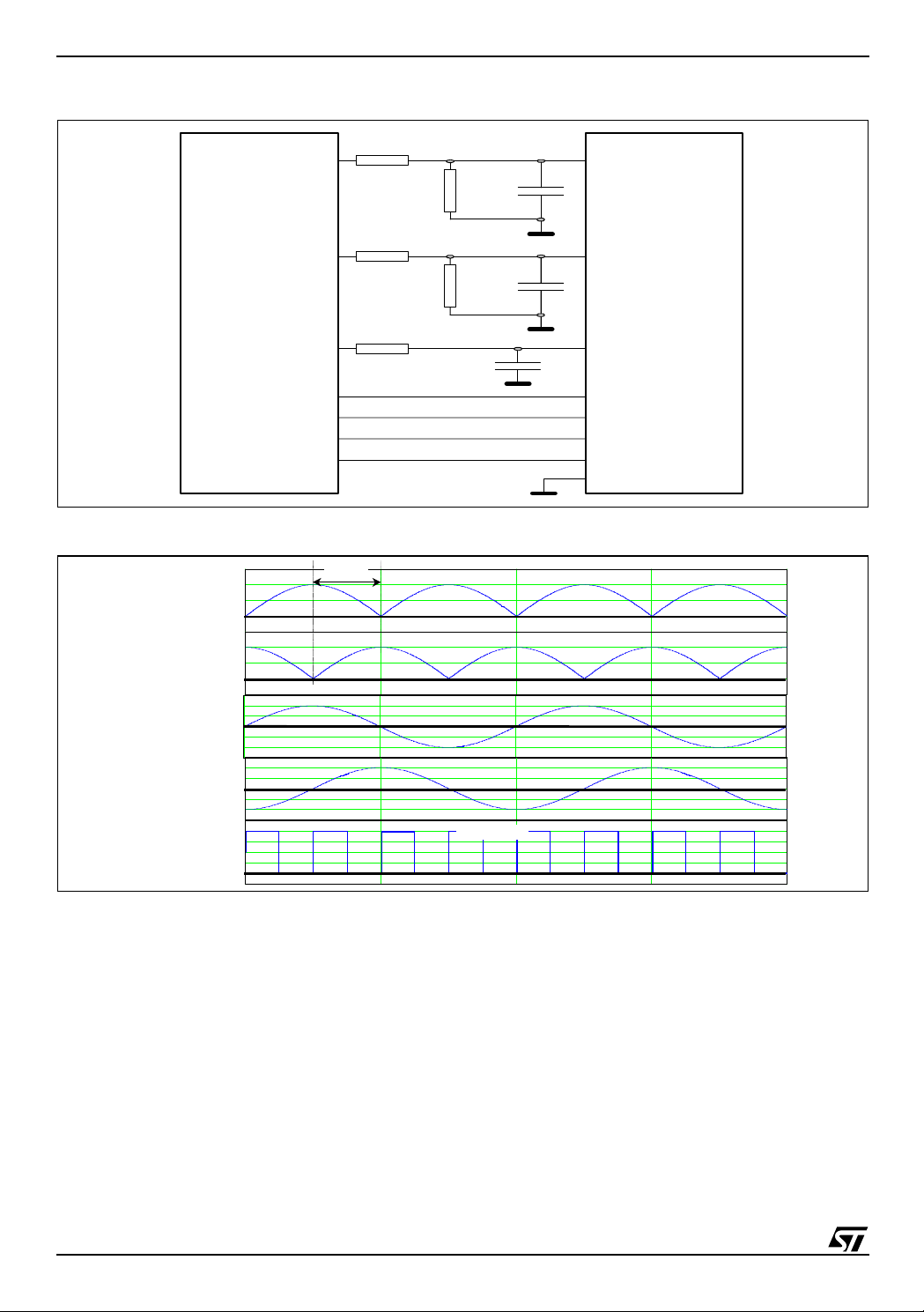
PractiSPIN is an evaluation and demonstratio n system that can be used with the Power SPIN family (L62X X) of
devices. A Graphical User Interface (GUI) (see Figure 34) program runs on an IBM-PC under windows and communicates with a common ST7 based interface board (see Figure 35) through the RS232 serial port. The ST7
interface board connects to a device spec ific ev aluation board (t arget board) via a standard 34 pin ribbon c able
interface.
Depending on the target device the PractiSPIN can drive a stepper motor, 1 or 2 DC motors or a brushless DC
(BLDC) motor, operatin g signific ant parameters such as SPEED, CURREN T, VOLTAGE, DIRECTIO N, ACCELERATION and DECELERATION RATES from a user friendly graphic interface, and programming a sequence
of movements.
The software also allows evaluating the power dissipated by the selected device and, for a given package and
dissipating copper area on the PCB, estimates the device's junction temperature.
Figure 34. PractiSPIN PC Software
31/43

AN1451 APPLICATION NOTE
Figure 35. PractiSPIN ST7 Evaluation Board
32/43

AN1451 APPLICATION NOTE
4.2 EVAL6208N
An evaluation board has been produced to help the evaluation of the device in PowerDIP package. It implements a typical application with several added components. Figure 37 shows the electrical schematic of the
board; in the table below the part list is reported.
CN1, CN2, CN3, CN4 2-poles connector R1 100Ω resistor
CN5 34-poles connector R2 820Ω 0.6W resistor
C1 220nF/100V Ceramic or Polyester capacitor R3, R4, R5, R6, R7, R8 10kΩ resistor
C2 220nF/100V Ceramic or Polyester capacitor R9 4.7kΩ resistor
C3 100µF/63V capacitor R10, R21 20kΩ 1% resistor
C4 10nF/100V Ceramic capacitor R11, R12 100kΩ trimmer
C5 10µF/16V Capacitor R13, R22 2.2kΩ resistor
C6 100nF Capacitor R14, R15, R16, R17, R18, R191Ω 0.4W resistor
C7, C8 68nF Capacitor R20, R24 5kΩ trimmer
C9, C10 820pF Capacitor S1 quad switch
D1, D2 1N4148 Diode U1 L6208N
D3 BZX79C5V1 5.1V Zener Diode JP1 3-pin jumper
The Evaluation Board provides ex ternal connectors for the supply voltage, an exter nal 5V reference for the logi c
inputs, four outputs for the motor and a 34-pin connector to control the main functions of the board through an
µ
external
The PractiSPIN tool is composed of a graphic interface software running on a PC that connects with the hardware based on the ST7 µC, which contains an upgradeabl e firmware. This tool allows a fast and easy eval uation
of the PowerSPIN family devi ces, giving the ability of setti ng the decay mode, the stepping sequence, th e output
current; to control the motor speed, acceleration and deceleration and to program a sequence of movements.
The PC-software also provides a Po wer Dissipa tion and Ther mal Analysi s secti on, intended to help a fas t evaluation of the device, package and dissipating copper area required by the user’s application, and to be a good
starting point designing an application (from the power dissipation and thermal point of view).
C board or the PractiSPIN tool.
Running the evaluation board in stand-alone mode, instead, four switches (S1) allow enabling the device, setting the direction of the rotation, the type of current decay, the stepping sequence. R20 and R24 set the reference voltage separately for the two bridges, while R13, C7 and R22, C8 are low-pass filters to provide an
external reference voltage by a PWM output of a
µ
C (see also the Microstepping section). Using external V
REF
inputs R10, R20, R21, R24 must be disconnected unless the PractiSPIN ST7 evaluation board is used. This
board, in fact, is provided with an offset cancellation circuitry trimmable thr ough a potentiometer (see PractiSPIN
documentation). R11, C9 and R12, C10 are used to set the off-time of the two channels of the IC.
The 5V voltage for logic inputs and for references (V
refA
and V
) is obtained from R2, D3. Depending on the
refB
supply voltage, the value of resistor R2 should be changed in order to ensure a correct biasing of D3.
The jumper JP1 allows choosing the 5V voltage from the internal zener diode network or pin 11 of CN5 (for ex-
ample an external µC board can provide 5V to the evaluation board). Also CN2 connector can be used to provide an external 5V voltage to the board (in that case R2, D3 should be disconnected). CN2, or pin 1 of CN5,
can also be used to provide a 5V voltage to external circuits (as, for example, the PractiSPIN ST7 board). In this
case the current that can be drawn form the board depends on the supply voltage and on R2 value.
Figure 38, Figure 39, Figure 40 show the component placement and the two layers layout of the L6208N Evaluation Board. A large GND area has been used, to g uarant ee minima l nois e and good p ower dis sipation for the
device.
33/43

AN1451 APPLICATION NOTE
Figure 36. EVAL6208N.
R8
C6
R9
JP1
R20
R24
R2
4.2.1 Important Notes
JP1 : close in INT position for use with PractiSPIN ST7 board
C6 : recommended change to 5.6 nF for safe Overcurrent protection
R8 : recommended change to 100 k for safe Overcurrent protection
R9 : recommended change to 100 k if EN pin is driven from the CN5 connector (for example with PractiSPIN
ST7 board) for safe Overcurrent protection
R20, R24 : set the maximum current obtainable through PractiSPIN (see PractiSPIN documentation)
R2 : recommended change to adequate value (depending on supply voltage) to obtain 5V across D3
4.2.2 Thermal Impedance
EVAL 6208N has been thermally characterized. Figure 41 shows the thermal impedance junction to ambient
and the pulsed thermal impedance junction to ambient. This characterization is valid for the device directly soldered into the PCB, without socket.
34/43

Figure 37. EVAL6208N Electrical schematic.
CN1
1
2
CN2
GND
2
1
D3
R2
CN3
1
2
CN4
AN1451 APPLICATION NOTE
1
2
CONTROL
CW/CCW
RE SET
RCA
EN
DIAG
HALF/FULL
CLOCK
PullUp
246810121416182022242628303234
C5
VCCREF
JP1
int.
ext.
+5V
C3
D2
R1
D1
2
PullUp
13
17
VSB
20
VSA
C4
22
VCP
15
C2
VBOOT
21
5
OUT1A
8
OUT1B
OUT2A
OUT2B
16
PullUp
U1
SENSEB
SENSEA
RCB
RCA
L6208N
19
GND
18
C1
S1
EN
9
10
11
12
8
7
CW
6
5
CCW
SLOW
13
14
4
3
FAST
15
16
HALF
FULL
2
1
PullUp
PullUp
GND
7
GND
6
GND
R8
R7
R6
R5
R4
R3
CW/CCW
CLOCK
2
1
CLOCK
HALF/FULL
CONTROL
12
13
VREFB
VREF A
RESET
EN
14
23
R9
DIAG
13579
10
3
RCB
9
4
RCA
11
VREF B
24
VREF A
C6
PullUp
+5V
RCA
C8
C7
R10
1113151719212325272931
R19
R18
R17
R16
R15
R14
R12
C9
R11
PullUp
R20
R13
VREFA
CW
CW
C10
CN5
33
VREF B
CLOCK
VRE FA
CW
R24
R21
CW
R22
VREFB
CLOCK
CW/CCW
CONTROL
EN
HALF/FULL
DIAG
RESET
35/43

AN1451 APPLICATION NOTE
p
Figure 38. EVAL6208N Component placement.
Figure 39. EVAL6208N Top Layer Layout.
Signal GND
Power GND
Ca
Bulk
acitor
36/43
Figure 40. EVAL6208N Bottom Layer Layout.
AN1451 APPLICATION NOTE
Short
SENS E path
Figure 41. EVAL6208N Thermal imped ance Ju nction to Ambient and pulsed Thermal impedance
Junction to Ambient.
40
35
30
25
Z
th J-A
20
[ºC/W]
15
10
5
0
1.1030.01 0.1 1 10 100 1.1031.10
Z
th J-A
time [s ]
4
Z
th J-A
[ºC/W]
40
35
30
25
20
15
10
1.10
Pulsed Z
DC=50%
DC=25%
DC=10%
5
0
3
0.01 0.1 1 10 100 1.1031.10
DC=5%
time [s]
th J-A
4
37/43

AN1451 APPLICATION NOTE
4.3 EVAL6208PD
An evaluation boar d has been pr oduced to help the evaluation of the devic e in PowerS O package. It implem ents
a typical application with several added components. Figure 43 shows the electrical schematic of the board; in
the table below the part list is reported.
CN1, CN2, CN3, CN4 2-poles connector R1 3.5kΩ 0.6W resist or
CN5 34-poles connector R2, R3, R4, R5, R6, R7 10kΩ resistor
C1 220nF/100V Ceramic or Polyester capacitor R3, R4, R5, R6, R7, R8 10kΩ resistor
C2 220nF/100V Ceramic or Polyester capacitor R8, R17 5kΩ trimmer
C3 100µF/63V capacitor R9, R19 2.2kΩ resistor
C4 10nF/100V Ceramic capacitor R10, R11 100kΩ trimmer
C5 10µF/16V Capacitor R12, R13, R14, R15 0.4Ω 1W resistor
C6, C9 68nF Capacitor R16, R20 20kΩ 1% resistor
C7, C8 820pF Capacitor R18 100Ω resistor
C12 100nF Capacitor R21 4.7kΩ resisto r
D1 BAT46SW Diodes S1 quad switch
D2 BZX79C5V1 5.1V Zener Diode U1 L6208PD
JP1 3-pin jumper
The Evaluation Board provides ex ternal connectors for the supply voltage, an exter nal 5V reference for the logi c
inputs, four outputs for the motor and a 34-pin connector to control the main functions of the board through an
external
µ
C board or the PractiSPIN tool.
The PractiSPIN tool is composed of a graphic interface software running on a PC that connects with the hardware based on the ST7 µC, which contains an upgradeabl e firmware. This tool allows a fast and easy eval uation
of the PowerSPIN family devi ces, giving the ability of setti ng the decay mode, the stepping sequence, th e output
current; to control the motor speed, acceleration and deceleration and to program a sequence of movements.
The PC-software also provides a Po wer Dissipa tion and Ther mal Analysi s secti on, intended to help a fas t evaluation of the device, package and dissipating copper area required by the user’s application, and to be a good
starting point designing an application (from the power dissipation and thermal point of view).
Running the evaluation board in stand-alone mode, instead, four switches (S1) allow enabling the device, setting the direction of the rotation, the type of current dec ay, the stepping sequenc e. R8 and R17 set the refer ence
voltage separately for the two bridges, while R 9, C6 and R19, C9 are low-pa ss filters to provide an external r eference voltage by a PW M output of a
µ
C (see also the Microsteppi ng sec tion). Us ing exte rnal V
inputs R16,
REF
R8, R20, R17 must be disconnected unl ess the P ractiSP IN ST7 eval uation board is used. This boar d, in fact, i s
provided with an offset cancellation circuitry trimmable through a potentiometer (see PractiSPIN documentation). R10, C7 and R11, C8 are used to set the off-time of the two channels of the IC.
The 5V voltage for logic inputs and for references (V
refA
and V
) is obtained from R1, D2. Depending on the
refB
supply voltage, the value of resistor R1 should be changed in order to ensure a correct biasing of D2.
The jumper JP1 allows choosing the 5V voltage from the internal zener diode network or pin 11 of CN5 (for ex-
ample an external µC board can provide 5V to the evaluation board). Also CN2 connector can be used to provide an external 5V voltage to the board (in that case R1, D2 should be disconnected). CN2, or pin 1 of CN5,
can also be used to provide a 5V voltage to external circuits (as, for example, the PractiSPIN ST7 board). In this
case the current that can be drawn form the board depends on the supply voltage and on R1 value.
Figure 44, Figure 45, Figure 46 show the component placement and the two layers layout of the L6208PD Evaluation Board. A large GND area has been used, to g uarant ee minima l nois e and good p ower dis sipation for the
device.
38/43

Figure 42. EVAL6208PD.
AN1451 APPLICATION NOTE
R7
C12
JP1
R17
R8
R1
R21
4.3.1 Important Notes
JP1 : close in INT position for use with PractiSPIN ST7 board
C12 : recommended change to 5.6 nF for safe Overcurrent protection
R7 : recommended change to 100 k for safe Overcurrent protection
R21 : recommended change to 100 k if EN pin is driven from the CN5 connector (for example with PractiSPIN
ST7 board) for safe Overcurrent protection
R8, R17 : set the maximum current obtainable through PractiSPIN (see PractiSPIN documentation)
R1 : recommended change to adequate value (depending on supply voltage) to obtain 5V across D2
4.3.2 Thermal Impedance
EVAL 6208PD has been thermally characterized. Figure 47 shows the thermal impedance junction to ambient
and the pulsed thermal impedance junction to ambient.
39/43

AN1451 APPLICATION NOTE
Figure 43. EVAL6208PD Electric al sch emat ic.
CN4
1
1
15
OUT1A
2
2
CW/CCW
RCA
DIAG
TOUTA0 P2.2
246810121416182022242628303234
1113151719212325272931
13579
ADC_REF
PullUp
22
32
20
5
OUT1 B
OUT2A
NC17NC
OUT2B
NC21NC23NC31NC34NC
SENSE B
SENSEA
RCB
35
U1
SENSEB
25
SENSEA
12
24
R11
+5V
R15
R14
R13
R12
CW
C8
CLOCK
CONTROL
TINB1 P2.5
TINA1 P2.4
TOUTA1 P2.6
OCMPA1 P4.2
CLOCK
HALF/FULL
CN5
CON34A
33
OCMPB1/ICAPB1 P4.3
VREFB
VREFA
EN
RESET
TOUTB1 P2.7
TINA0 P2.0
TOUTB0 P2.3
R1
R18
ext.
+5V
CN2
1
2
D2
C5
JP1
JUMPER 3x1
int.
2
PullUp
13
C3
33
VSB
4
VSA
C4
7
VCP
CN1
1
2
VCCREF
VIN
1 3
D1
2
CN3
16
NC2NC3NC6NC14NC
PullUp
40/43
VREF _A
PullUp
R8
R9
C7
CW
CW
R20
R17
CW
R19
VREF_B
RCA
30
R7
R6
R5
R4
19
18
36
1
CLOCK
VBOOT
GND
GND
GND
GND
L6208PD
HALF/FULL
CONTROL
CW/CCW
CLOCK
EN
10
CLOCK
28
11
CW/CCW
27
29
EN
CONTROL
HALF/FULL
C1
C2
S1
EN
9
10
CW
11
12
CCW
SLOW
13
14
FAST
HALF
15
16
FULL
PullUp
PullUp
GND
8
7
6
5
4
3
2
1
R3
R2
VREF B
VREF A
RESET
R21
RCA
8
RESET
13
26
9
C12
PullUp
DIAG
R10
C9
VREF B
C6
VREF A
R16

Figure 44. EVAL6208PD Component placement.
AN1451 APPLICATION NOTE
Figure 45. EVAL6208PD Top Layer Layout.
41/43
AN1451 APPLICATION NOTE
Figure 46. EVAL6208PD Bottom Layer L ayou t .
Figure 47. EVAL6208PD Thermal impedance Junction to Ambient and pulsed Thermal impedance
Junction to Ambient.
25
20
15
Z
th J-A
[ºC/W]
10
5
0
1.1030.01 0.1 1 10 100 1.1031.10
42/43
Z
time [s]
th J-A
25
20
15
Z
th J-A
[ºC/W]
10
4
1.10
DC=50%
DC=25%
5
DC=10%
0
3
0.01 0. 1 1 10 100 1.1031.10
Pulsed Z
DC=5%
time [s]
th J-A
4

AN1451 APPLICATION NOTE
5 REFERENCES
1] D. Arrigo, A. Genova, T. Hopkins, V. Marano, A. Novelli, "A New Fully Integrated Stepper Motor Driver IC",
Proceedings of PCIM 2001, September 2001, Intertech Communication.
2] H. Sax, "Stepper Motor Driving" (AN235).
3] T. Hopkins, "Controlling Voltage Transients in Full Bridge Driver Applications" (AN280).
4] T. Hopkins, "Stepper Motor Drive Considerations, Common Problems and Solutions" (AN460).
5] T. Hopkins, K. Kim, "Microstepping Stepper Motor Drive Using Peak Detecting Current Control" (AN1495).
6] P. Casati and C. Cognetti, "A New High Power IC Surface Mount Package Family" (AN668)
Information furnished is believed to be accurate and reliable. However, STMicroelectronics assumes no responsibility for the consequences
of use of such information nor for any infringement of patents or other rights of third parties which may result from its use. No license is granted
by implic ation or otherwise under any patent or patent r i ght s of STMi croelectr oni cs. Specifications menti oned in thi s publicati on are subj ect
to change without notice. This publication supersedes and replaces all information previously supplied. STMicroelectronics products are not
authorized for use as cri tical components in li f e support dev i ces or systems without express writ t en approval of STMicroel ectronics.
The ST logo is a registered trademark of STMi croelectr oni cs.
All other n am es are the property of th ei r respective owners
© 2003 STMi croelectronics - All ri ght s reserve d
Australi a - B elgium - B razil - Canada - China - Czech Republ i c - Finland - F rance - Germ any - Hong Kong - India - Is rael - Italy - Japan -
Malaysia - Malta - Morocco - Singapore - Spain - Sweden - Switzerland - United Kingdom - United States
STMicroelectronics GROUP OF COMPANIES
www.st.com
43/43
 Loading...