

Page 1

AN1449
Application note
ST6200C
universal motor drive software
Introduction
This application note describes the software of a low-cost phase-angle motor control drive
system based on an OTP version of the ST6200C microcontroller and a BTB16-600CW
snubberless triac. The application has been developed by STMicroelectronics and is
available as a low-cost evaluation board UMC01EVAL.
This board can be widely used in many applications such as vacuum cleaners, power tools,
food processors and lighting dimmers. The microcontroller implements the following
functions:
■ Speed control: the motor speed is set by a potentiometer on the board. With a look up
table, the MCU can convert speed commands to firing angle delay times. The power
delivered to the motor can be adjusted by changing the firing angle with reference to the
voltage zero crossing signal.
■ Soft start: This reduces the motor inrush current at start-up.
■ Mains period measurement: In order to reduce system cost, a RC oscillator is used on the
UMC01EVAL board as the MCU clock source. However its frequency can vary up to +/20% because it is highly dependent on power supply voltage and temperature. To control
the motor accurately, the mains power line period is measured and used as a time base.
June 2010 Doc ID 8325 Rev 2 1/14
www.st.com
Page 2

Contents AN1449
Contents
1 Hardware description . . . . . . . . . . . . . . . . . . . . . . . . . . . . . . . . . . . . . . . . 4
1.1 General information . . . . . . . . . . . . . . . . . . . . . . . . . . . . . . . . . . . . . . . . . . 4
1.2 Board schematics . . . . . . . . . . . . . . . . . . . . . . . . . . . . . . . . . . . . . . . . . . . . 4
2 Main program . . . . . . . . . . . . . . . . . . . . . . . . . . . . . . . . . . . . . . . . . . . . . . . 5
2.1 RC oscillator . . . . . . . . . . . . . . . . . . . . . . . . . . . . . . . . . . . . . . . . . . . . . . . . 5
2.2 Mains period measurement . . . . . . . . . . . . . . . . . . . . . . . . . . . . . . . . . . . . 5
2.3 Timing definition of main program . . . . . . . . . . . . . . . . . . . . . . . . . . . . . . . 5
3 Gate pulses . . . . . . . . . . . . . . . . . . . . . . . . . . . . . . . . . . . . . . . . . . . . . . . . 7
3.1 General description . . . . . . . . . . . . . . . . . . . . . . . . . . . . . . . . . . . . . . . . . . 7
3.2 Phase angle calculation . . . . . . . . . . . . . . . . . . . . . . . . . . . . . . . . . . . . . . . 7
3.3 Gate pulse generation . . . . . . . . . . . . . . . . . . . . . . . . . . . . . . . . . . . . . . . . 7
3.4 Interrupt servicing time . . . . . . . . . . . . . . . . . . . . . . . . . . . . . . . . . . . . . . . . 7
4 Subroutines . . . . . . . . . . . . . . . . . . . . . . . . . . . . . . . . . . . . . . . . . . . . . . . . 9
4.1 Power on reset . . . . . . . . . . . . . . . . . . . . . . . . . . . . . . . . . . . . . . . . . . . . . . 9
4.2 Soft start . . . . . . . . . . . . . . . . . . . . . . . . . . . . . . . . . . . . . . . . . . . . . . . . . . . 9
4.3 Conclusion . . . . . . . . . . . . . . . . . . . . . . . . . . . . . . . . . . . . . . . . . . . . . . . . . 9
5 Revision history . . . . . . . . . . . . . . . . . . . . . . . . . . . . . . . . . . . . . . . . . . . 10
Appendix A Power on reset flowchart . . . . . . . . . . . . . . . . . . . . . . . . . . . . . . . . . 11
Appendix B Main program flowchart . . . . . . . . . . . . . . . . . . . . . . . . . . . . . . . . . . 12
1
Appendix C Soft start flowchart . . . . . . . . . . . . . . . . . . . . . . . . . . . . . . . . . . . . . . 13
2/14 Doc ID 8325 Rev 2
Page 3

AN1449 List of figures
List of figures
Figure 1. UMC01EVAL board schematics . . . . . . . . . . . . . . . . . . . . . . . . . . . . . . . . . . . . . . . . . . . . . . 4
Figure 2. Timing definition of main program . . . . . . . . . . . . . . . . . . . . . . . . . . . . . . . . . . . . . . . . . . . . 6
Figure 3. Power on reset flowchart . . . . . . . . . . . . . . . . . . . . . . . . . . . . . . . . . . . . . . . . . . . . . . . . . . 11
Figure 4. Main program flowchart . . . . . . . . . . . . . . . . . . . . . . . . . . . . . . . . . . . . . . . . . . . . . . . . . . . 12
Figure 5. Soft start flowchart . . . . . . . . . . . . . . . . . . . . . . . . . . . . . . . . . . . . . . . . . . . . . . . . . . . . . . . 13
Doc ID 8325 Rev 2 3/14
Page 4
Hardware description AN1449
VCC
VCC
U1
ST62T00
1
2
3
4
5
6
7
8 9
10
11
12
13
14
15
16
VDD
OSCIN
OSCOUT
NMI
VPP/TEST
RST
PB7/AIN4
PB6/AIN3 PB5/AIN2
PB3/AIN1
PB1
PB0
PA3
PA2
PA1
VSS
R7
220K
R6
220K
R4
47K
Q1
BTB16-600CW
R5
470R/1W
C3
470nF/400V
C1
100nF
C2
220uF/16V
D2 1N4148
SPEED
10K
R1
1R/2W
F1
FUSE 10A
D1
BZX85C5.6
R2 3K
C4
100nF
R3 150R
LINE
NEUTRAL
MOTOR
J1
J3
J4
J2
16Pin Socket
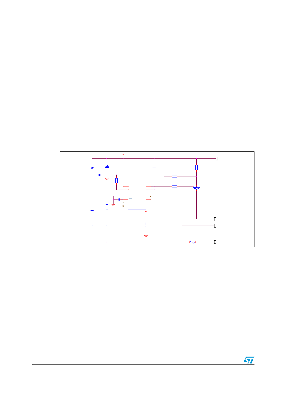
1 Hardware description
1.1 General information
The schematics of universal motor control board are shown in Figure 1. On this board, a low
cost capacitive power supply generates +5 V voltage for the ST62T00C MCU and its
application circuit. The motor speed control is managed by the ST62T00C 8-bit MCU. The
MCU clock is generated by on-board RC network. The internal 8-bit timer is used for the
triac triggering control. The voltage zero crossing event is detected by two current limiting
resistors (R6 & R7). The microcontroller triggers the snubberless triac BTB16-600CW
directly with its 20 mA outputs. Three high sink outputs can supply 60 mA gate currents
(I
GT=35 mA). This board is able to drive a universal motor up to 1500 W.
1.2 Board schematics
Figure 1. UMC01EVAL board schematics
The hardware environment of the MCU has the following features:
● The MCU oscillator is implemented by an on-board RC network.
● No external reset circuit is used, this function is handled by the low voltage detector
option of the ST62T00C.
● The voltage zero crossing event is detected through current limiting resistors (R6 &
R7).
● R1 is reserved for future use. It must be replaced by a jumper when the board is
running in open loop mode. In closed loop, it is used as a shunt resistor. It can measure
the motor peak current.
4/14 Doc ID 8325 Rev 2
Page 5

AN1449 Main program
2 Main program
2.1 RC oscillator
In most applications, the MCU internal clock is supplied by a quartz crystal or a ceramic
resonator. On this board, for cost reasons, it has been chosen to generate the system clock
with an external resistor (the capacitor is implemented internally). However as a result of this
choice, clock accuracy is only about +/-20% because the RC oscillator frequency is highly
dependent on supply voltage and temperature variations. For more details, please refer to
the “clock and timing characteristics” section of the ST6200C datasheet.
2.2 Mains period measurement
To obtain a more accurate clock source for driving the motor, the AC power line period is
measured by the microcontroller. It is used as a system clock reference. The voltage zero
crossing detection is performed by the ST62T00C NMI interrupt with two current limiting
resistors (R6 & R7).
Note: For the ROM version, as the injection is forbidden on the NMI pin, it is recommended to use
another pin with interrupt capability.
The interrupt (falling edge only) is generated at each negative voltage zero crossing event. It
triggers the internal 8-bit Timer Counter Register (TCR) to measure the power line period.
The result is stored in the T50HZ register. In 220 V/50 Hz applications, the value of T50HZ
register corresponds to 20 ms when the timer input clock division factor in the Timer Status
Control Register (TSCR) is 64. The same value corresponds to 10 ms when the timer input
clock division factor is 32.
2.3 Timing definition of main program
The basic principle of the phase angle control algorithm is very simple. The ST62T00C can
detect the beginning of a full wave by detecting the negative voltage zero crossing event,
after which it can calculate the phase angle, load the phase delay time PHASE in the 8-bit
Timer Counter Register (TCR) and start the timer counting.
When the timer expires, the Timer Counter Register (TCR) is reloaded with a value in
T50NEW register which is equivalent to the duration of one half cycle (e.g. 10 ms at 50 Hz),
after which the first TRIAC triggering pulse is generated. Be aware that the value in the
T50HZ register must be compensated with a look up table (RCTAB) in order to eliminate the
fluctuation of the RC oscillator frequency within one full wave cycle. The compensated value
is stored in the T50NEW register. To obtain the duration of a half cycle, we can use the
same value in the T50NEW register and divide the corresponding timer input clock
frequency by 2. It can be easily implemented by selecting the division factor of prescaler bits
in the Timer Status Control Register (TSCR).
The time base T50HZ of the power line period is averaged every 16 full wave cycles (e.g.
320 ms at 50 Hz) in order to eliminate the influence of the RC oscillator. After that, the
potentiometer measurement is performed with the internal A/D converter. The new speed
command goes through the ramp up or down subroutine and speed look up table
(VREFTB). The new phase angle in the PHASE register for the next cycle is computed. In
addition, as mentioned above, the full wave timer value in register T50HZ must be
Doc ID 8325 Rev 2 5/14
Page 6

Main program AN1449
Triac Pulse
Timer
PHASE T50NEW DELTAT
NMI
Mains Voltage
PA1/PA2/PA3
ZVC Interrupt
Get DELTAT
Reload Timer
Timer Interrupt
Reload Timer
Fire TRIAC
T50HZ Update
Perform ADC
Soft Start
Calculate PHASE
Timer Interrupt
Measure DELTAT
Fire TRIAC
MAINS PERIOD
compensated with the look up table (RCTAB) at different phase angles. This new value is
stored in the T50NEW register.
When the half-cycle timer reaches zero, the second triac triggering pulse is generated. After
that, the timer counter register (TCR) is reloaded with 255 and starts counting. It is used as
a capture to measure the duration from the second triggering pulse to the next voltage zero
crossing event.
When the next voltage zero crossing interrupt occurs, the timer will be stopped by software.
The duration from the second gate pulse to the zero crossing interrupt is stored in the
DELTAT register. The full wave time will be equal to the sum of DELTAT, T50NEW and
PHASE.
In total, one mains full wave period is divided into three parts: phase angle (PHASE
register), half wave period (T50NEW register) and the rest (DELTAT register). The timing
definition of main program is shown in the following figure.
Figure 2. Timing definition of main program
6/14 Doc ID 8325 Rev 2
Page 7

AN1449 Gate pulses
PHASE
T50Hz Vref×
256
------------------------------------- -=
3 Gate pulses
3.1 General description
The gate current pulses are generated during the main program (refer to Figure 2).
Appendix A gives the flowchart of the main program. As soon as a ZVC event is detected,
the ST62T00C reloads the timer with the phase angle delay time and starts the timer. When
the timer reaches zero, the first gate triggering pulse is generated. The timer is reloaded and
enabled with a value of one half-cycle. When the timer reaches zero, the second gate
triggering pulse is generated within one full wave cycle.
3.2 Phase angle calculation
To eliminate the timer clock variations due to voltage and temperature drift, the timer clock
must be synchronized with the line voltage zero crossing. The power line period is
measured by the ST62T00C internal 8-bit timer. The resulting half cycle period is stored in
the T50HZ register and used as the system clock. This number is then divided by 256, which
results in 256 steps per half wave. With this division, 256 discrete phase angles are
possible. This results in a resolution of 0.7 degrees. The actual phase angle PHASE is
calculated as follows:
Dividing by 256 is simply implemented by considering the most significant byte of the
multiplication result of T50Hz and speed reference (Vref). A look-up table relating the delay
time to the power requirement contains 64 different levels. The conduction time of the triac
can be varied from 1.6 ms to 9.2 ms for a 50 Hz application. The user can easily adjust the
minimum and maximum power levels by changing the look up table.
3.3 Gate pulse generation
A universal motor is an inductive load. The motor current and input voltage are not in phase.
The triac will turn off at the current zero crossing. To reduce component cost, the phase shift
between current and voltage is not measured but can be adjusted by defining the maximum
speed constant v_max. This constant should be decreased if the phase shift between
voltage and current is too large.
3.4 Interrupt servicing time
The timer is not started immediately when an interrupt request occurs. This is because
some instructions are executed before starting the timer. For example, before starting to
count the first phase angle time, the program must run the NMI interrupt routine, save the
DELTAT result, reload the timer and restart the timer. This takes 33 CPU cycles. To take the
code execution time into account, we should convert it to the timer counter value (Tcode).
As we know, the MCU oscillator frequency (f
Therefore, “N” CPU cycles execution time is 13xN/f
frequency (f
) is divided by 12 to drive the internal timer, and then it is divided by the
CPU
) is divided by 13 to drive the CPU core.
CPU
CPU seconds. The MCU oscillator
Doc ID 8325 Rev 2 7/14
Page 8

Gate pulses AN1449
Tcode
N13×
fcpu
----------------- -
fcpu
12 32×
--------------------
× N
13
384
--------- -
×==
division factor programmed in the TSCR register. In this software, the division factor is 32
during the main program. Therefore, one unit timer counter equals 12x32/f
seconds. We
CPU
can easily work out the relationship between N cycles of code execution time and the timer
counter value (Tcode), as shown below:
For example, the code execution time for 33 cycles approximately equals one unit of the
timer count.
8/14 Doc ID 8325 Rev 2
Page 9

AN1449 Subroutines
4 Subroutines
4.1 Power on reset
After each RESET interrupt, a complete initialization procedure is executed. This subroutine
configures the port A & Port B, timer, A/D converter, interrupt option register and status flag
registers. It waits 100 ms for the supply stabilization, and then it measures the mains period.
The flowchart of this subroutine is shown in Appendix A.
4.2 Soft start
The soft start subroutine is entered when an acceleration or deceleration event occurs. The
soft start feature enhances the life of bulbs, reduces coil stresses in motors, and extends the
life of most loads. It can reduce the inrush current and prevent voltage fluctuations and
flicker in the power supply (refer to Flicker Norm EN61000-3-3).
This subroutine in fact changes the slope of the speed command. The slope is the same for
the accelerating and decelerating edge. It can be modified by changing the step constant.
This flowchart is shown in Appendix C.
4.3 Conclusion
This application note describes the software of a low cost universal motor control system. It
is intend to help you to use this software as a basis for developing your own motor drive and
to adapt it to your own requirements. The software is tested with the Raisonance RIDE ST6
Version 6.0.1 Assembler. For other assemblers the software must be adapted.
Doc ID 8325 Rev 2 9/14
Page 10

Revision history AN1449
5 Revision history
Table 1. Document revision history
Date Revision Changes
Oct-2001 1 Initial release
Format of the document modified.
Modified introduction on first page (reference to OTP version of the ST6200C
07-Jun-2010 2
added)
Replaced ST62T00C with ST6200C.
Added note in Section 2.2: Mains period measurement on page 5.
10/14 Doc ID 8325 Rev 2
Page 11

AN1449 Power on reset flowchart
RESET
PORT A & B Configuration
Inte rrupt O ption R e gister
Initialisation
Wait 100 ms
MAIN_PROG
Tim er & A D C Initialisation
Measure Mains Period
(T50H z)
Registers Initialisation
Status Flag Initialisation
Set Minimum Motor Speed
Phase Angle Calculation
Appendix A Power on reset flowchart
Figure 3. Power on reset flowchart
Doc ID 8325 Rev 2 11/14
Page 12

Main program flowchart AN1449
MAIN_PROG
Wait for ZVC event
Save TCR in DELTAT
Load Timer with Phase Angle
Restart Timer
Wait for Timer
Interrupt
Load Timer with T50NEW
Restart Timer
Generate TRIAC Triggering
Pulse on PA1/PA2/PA3
Make the average of T50HZ
Update T50HZ Register
Configure and Perform
A/D Converter
Get New Speed Command
MVNEW
Process Acceleration or
Deceleration Soft Start
16 times full wave
cycles passed?
Yes
No
Get Next Speed Command
MVOLD
Process Speed
Look Up Table
Calculate the next phase
angle time (PHASE)
Make Half Cycle Time
Symmetrical Compensation
T50NEW
Wait for Timer
Interrupt
Configure Timer to Measure
DELTAT
Generate TRIAC Triggering
Pulse on PA1/PA2/PA3
MAIN_PROG
Appendix B Main program flowchart
Figure 4. Main program flowchart
12/14 Doc ID 8325 Rev 2
Page 13

AN1449 Soft start flowchart
SOFT START
Process Ramp Up
Accelerate or
Decelerate Process?
SPEED PROCESS
Accelerate
Process Ramp Down
Decelerate
Within A/D
Converter Accuracy?
Within A/D
Converter Accuracy?
Within one Step Range? Within one Step Range?
MVOLD = MVOLD + STEP MVOLD = MVOLD - STEP
Yes Yes
No
No
No
No
MVOLD = MVNEW
Get New Speed Command
MVNEW
Appendix C Soft start flowchart
Figure 5. Soft start flowchart
Doc ID 8325 Rev 2 13/14
Page 14

AN1449
Please Read Carefully:
Information in this document is provided solely in connection with ST products. STMicroelectronics NV and its subsidiaries (“ST”) reserve the
right to make changes, corrections, modifications or improvements, to this document, and the products and services described herein at any
time, without notice.
All ST products are sold pursuant to ST’s terms and conditions of sale.
Purchasers are solely responsible for the choice, selection and use of the ST products and services described herein, and ST assumes no
liability whatsoever relating to the choice, selection or use of the ST products and services described herein.
No license, express or implied, by estoppel or otherwise, to any intellectual property rights is granted under this document. If any part of this
document refers to any third party products or services it shall not be deemed a license grant by ST for the use of such third party products
or services, or any intellectual property contained therein or considered as a warranty covering the use in any manner whatsoever of such
third party products or services or any intellectual property contained therein.
UNLESS OTHERWISE SET FORTH IN ST’S TERMS AND CONDITIONS OF SALE ST DISCLAIMS ANY EXPRESS OR IMPLIED
WARRANTY WITH RESPECT TO THE USE AND/OR SALE OF ST PRODUCTS INCLUDING WITHOUT LIMITATION IMPLIED
WARRANTIES OF MERCHANTABILITY, FITNESS FOR A PARTICULAR PURPOSE (AND THEIR EQUIVALENTS UNDER THE LAWS
OF ANY JURISDICTION), OR INFRINGEMENT OF ANY PATENT, COPYRIGHT OR OTHER INTELLECTUAL PROPERTY RIGHT.
UNLESS EXPRESSLY APPROVED IN WRITING BY AN AUTHORIZED ST REPRESENTATIVE, ST PRODUCTS ARE NOT
RECOMMENDED, AUTHORIZED OR WARRANTED FOR USE IN MILITARY, AIR CRAFT, SPACE, LIFE SAVING, OR LIFE SUSTAINING
APPLICATIONS, NOR IN PRODUCTS OR SYSTEMS WHERE FAILURE OR MALFUNCTION MAY RESULT IN PERSONAL INJURY,
DEATH, OR SEVERE PROPERTY OR ENVIRONMENTAL DAMAGE. ST PRODUCTS WHICH ARE NOT SPECIFIED AS "AUTOMOTIVE
GRADE" MAY ONLY BE USED IN AUTOMOTIVE APPLICATIONS AT USER’S OWN RISK.
Resale of ST products with provisions different from the statements and/or technical features set forth in this document shall immediately void
any warranty granted by ST for the ST product or service described herein and shall not create or extend in any manner whatsoever, any
liability of ST.
ST and the ST logo are trademarks or registered trademarks of ST in various countries.
Information in this document supersedes and replaces all information previously supplied.
The ST logo is a registered trademark of STMicroelectronics. All other names are the property of their respective owners.
© 2010 STMicroelectronics - All rights reserved
STMicroelectronics group of companies
Australia - Belgium - Brazil - Canada - China - Czech Republic - Finland - France - Germany - Hong Kong - India - Israel - Italy - Japan -
Malaysia - Malta - Morocco - Philippines - Singapore - Spain - Sweden - Switzerland - United Kingdom - United States of America
www.st.com
14/14 Doc ID 8325 Rev 2
 Loading...