


AN1447
APPLICATION NOTE
SOFTWARE DRIVER F OR
4-MULTIPLEXED LCD WITH A STANDARD ST62
by Microcontroller Division Applications
DESCRIPTION
This note describes a technique for driving a 4-multiplexed Liquid Crystal Display (LCD) with
a standard ST62 microcontroller (MCU), without any dedicated LCD driver peripheral. This
technique offers a display capability for applications which require a small display at a low cost
together with the versatile capabilities of the standard ST62xx MCU.
Higher display requirements are easily handled by dedicated members of the ST62 MCU
family, for example the ST6240. Solutions on how to use a standard ST6 to drive an LCD with
a multiplexing ratio of 2 (duplex) can be found in Application Note AN594.
The first sect ion of this not e describ es the typic al wavefo rms re quired to driv e an LCD, fi rst
without multiplexing (“direct” drive), then with a multiplexing rate of 4. The second section explains how to use a software library written in assembly language (MAST6 syntax) implementing a solution based on a standard ST62 MCU driving directly the LCD.
The program size and the CPU time occupation due to the LCD drive are minimized. Consequently many additional tasks can be added to the MCU program. Only few cheap additional
components are required.
AN1447/0901 1/26
1
4-MULTIPLEXED LCD WITH A STANDARD ST62
1 LCD DRIVING PRINCIPLES
1.1 LCD REQUIREMENTS
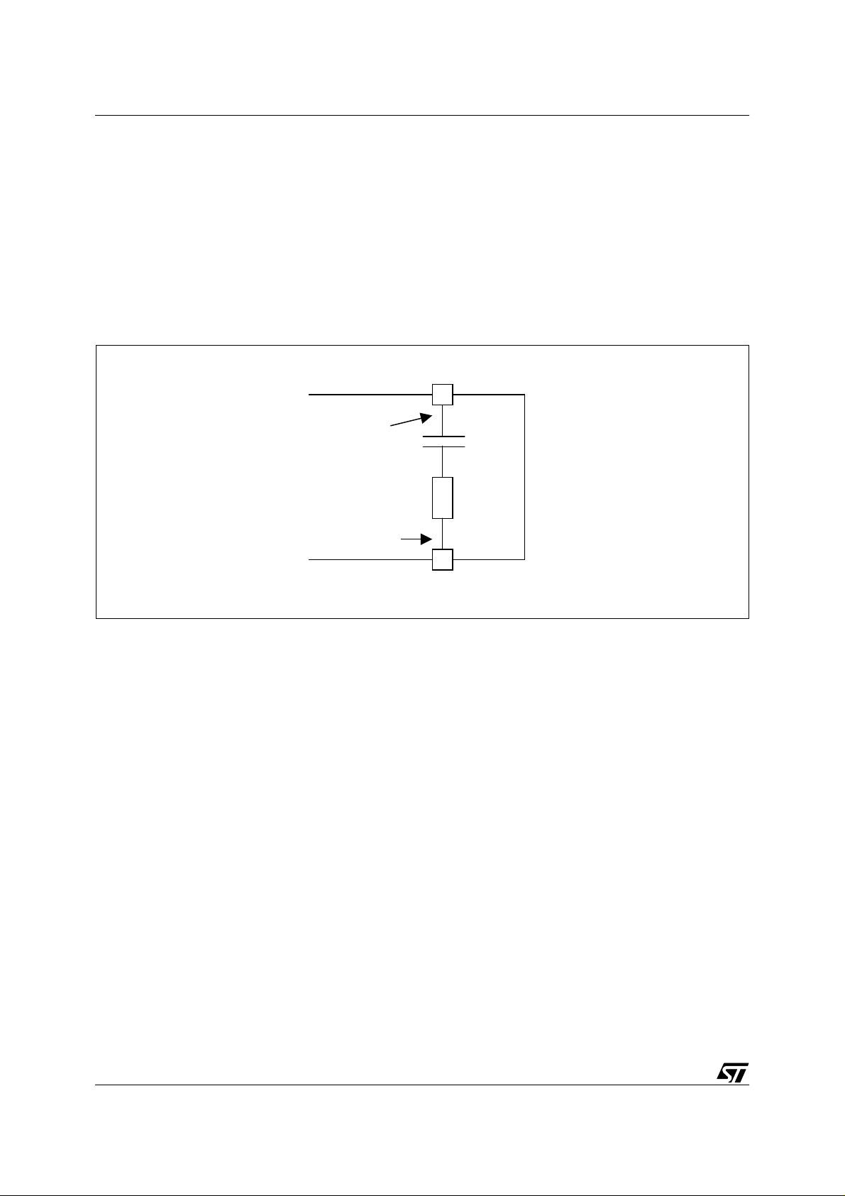
An LCD segment can either be transparent (“off”) or opaque (“on”), depending on the voltage
COM
applied to it. On Figure 1, this voltage is the di fference between
LCDs (ref lective pos itive d isplay s) an o paq ue segm e nt is se en dark and a tra nsp aren t seg ment is seen clear (same colour as the background).
Figure 1. Equivalent Electrical Schematic of an LCD Segmen t
and S voltages. On most
segment
electrode
backplane
S
C
R
s
COM
If no voltage is applied to it, a segment is transparent. To make it opaque, the LCD driver must
apply an AC voltage which Root Mean Square (RMS) value is above a certain threshold. This
voltage threshold depends on the LCD characteristics.
Segment voltage must also comply with the following conditions:
– Its absolute DC (mean) value must be very low (under 100 mV typically). Otherwise, the life
time of the LCD can be shortened.
– Its frequency must be in the range 30 – 2000 Hz typical ly. If too low, the disp lay flickers. If
too high, driving generates more power consumption.
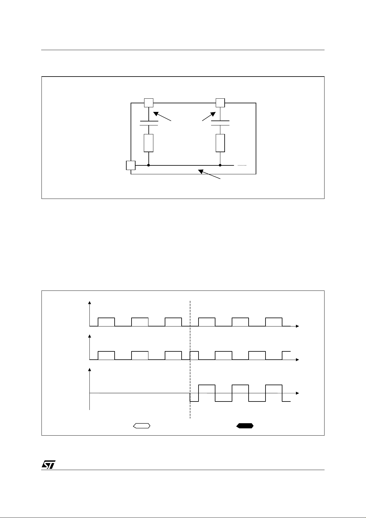
1.2 DIRECT LCD DRIVE
Each LCD segment is located between a segment electrode and a bac kplane common to al l
N
the segments (see Figure 2). Therefore, a display using
connections:
2/26
N
“segment electrode” pins (S0, S1,…) and 1 “common” pin (COM).
segments contains (N+1) external
2
4-MULTIPLEXED LCD WITH A STANDARD ST62
d
0
d
0
d
0
d
Figure 2. Connections inside a direc t drive L CD
S
0
S
…
1
segment
electrodes
COM
backplane
All these pins are connected to MCU I/O pins operating in output mode, either at l ogic level 0
or at logic level 1.
COM
The backplane is driven with a signal
controlled between 0 and
50%.
When se lectin g a segm ent ON , a sign al with oppos ite po larity to
sponding segment electrode pin. When the non-inverted signal
electrode pin, the segment is OFF.
V
with a duty cycle of
DD
COM
is sent to the corre-
COM
is sent to the segment
Figure 3. LCD signals for non-multiplexed drive
COM
V
d
S
V
d
S∆
= COM - S
S
V
d
-V
d
Note: on Figure 3,
(
S∆)
RMS
S
signal is the “segment electrode voltage” and
∆
= 0 ⇒ segment OFF
(
S∆)
RMS
= V
⇒ segment ON
dd
t
t
t
S
the “segment voltage”.
∆
3/26
4-MULTIPLEXED LCD WITH A STANDARD ST62
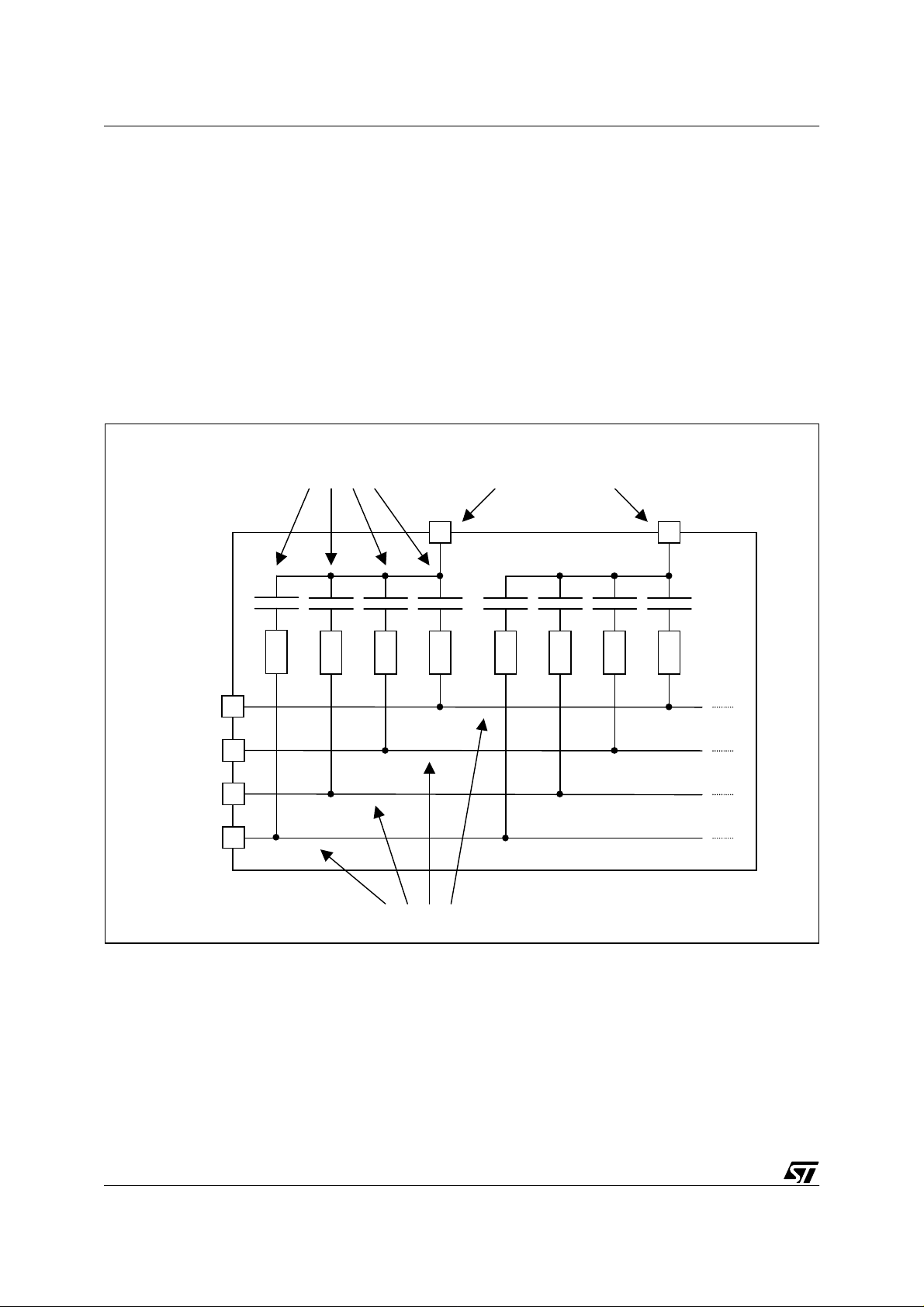
1.3 4-MULTIPLEXED LCD DRIVE
For 4-multiplexed drive, four backplanes are used instead of one. The LCD segments are
equally distributed between the four backplanes. They form groups of 4 segments, where
each segment is allocated to a different backplane. All the segment electrodes (or frontplane
electrodes) belonging to the same group are connected to a single external pin. Thus, a dis-
N
play using
segments contains (N/4+4) external connections:
ment electrodes (S
, S1,…) and 4 “common” pins (COM0, COM1, COM2 and COM3). On the
0
N/4
pins driving groups of seg-
rest of this document, the pins driving groups of segment electrodes are called “frontplane
pins”.
Figure 4. Connections inside a 4-multiplexed LCD
COM
COM
COM
COM
segment
electrodes
S
3
2
1
0
pins driving groups of
segment electrodes
0
S
…
1
backplanes
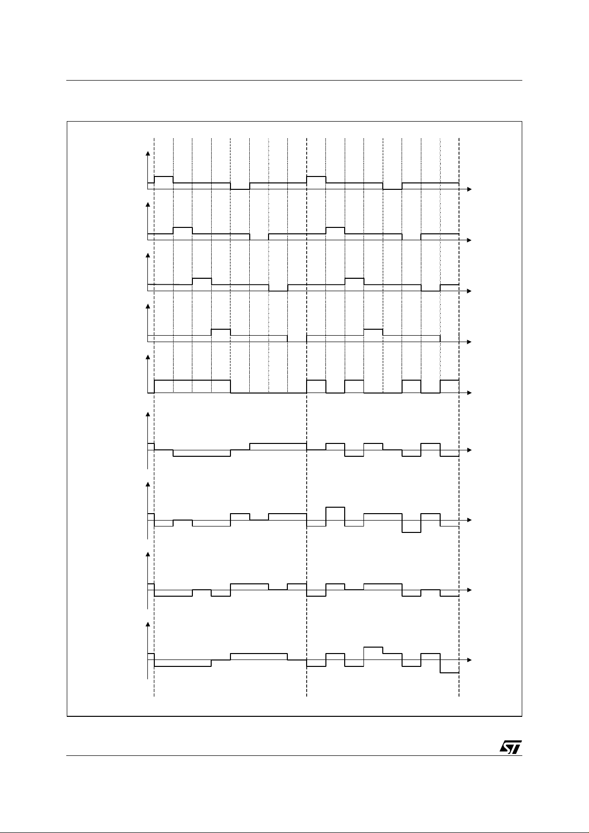
Three different voltage levels have to be generated on the backplanes: 0,
frontplane voltage levels are 0 and
V
only. Figure 5 shows typical backplane, frontplane and
DD
segment voltage waveforms.
Each period is divided into 8 phases ϕ
continuously, whereas
on S during phase ϕ
4/26
S
waveforms de pend on the r equired display. T he logic level ap plied
is the negation of the one applied during phase ϕ0, and so on for ϕ5 and
4
to ϕ7. Like in direct drive,
0
COM
waveforms are applied
V
DD
/2 and
V
. The
DD
4-MULTIPLEXED LCD WITH A STANDARD ST62
ϕ1, ϕ6 and ϕ5, ϕ7 and ϕ3. Changing the levels applied during phases ϕ0 and ϕ4 does not
change the DC value nor the RMS of
value of
S
voltage, but affects its RMS, as explained in Table 1.
∆
0
S
, S
and
S
∆
1
∆
2
voltages. It does not change the DC
∆
3
Table 1. How to switch on e segment on and off in 4-multiplexe d d rive
S
waveform
H during ϕ0, L during ϕ
L during ϕ0, H during ϕ
Segment S
DC RMS state DC RMS state
4
4
0 (√3/4).V
0 (√7/4).V
DD
DD
0
OFF 0
ON 0
Other segments
only depend on the rest
of
S
waveform
Note that even if a segment is OFF, its RMS voltage is not zero. As a result, contrast is not as
good as in direct drive. In addition, there is a risk of cross-talk (or ghosting): if segment voltage
(
S
) frequency is too high, a s egment c an become opaq ue ev en though the RMS voltage is
∆
i
below the threshold. So make sure that the driving frequency (considering the whole cycle, i.e.
the 8 phases) is under 2000 Hz ty pically.
V
The intermediate voltage
connected to the backplanes are configured by software to output mode for 0 or
to high impeda nce i nput mod e fo r
/2 is only required for the backplane voltages. The ST62 I/O pins
DD
V
levels o r
dd
V
/2. This inte rmedia te vol tage i s defi ned by two eq ual-
DD
valued resistors externally connected to the I/O pin.
By using an MCU w ith flexible I/O pi n confi guration such as a standa rd ST 62, 4-multip lexed
LCD drive can be made with only 8 additional resistors.
5/26
4-MULTIPLEXED LCD WITH A STANDARD ST62
d
d
d
d
d
d
d
d
d
d
d
d
d
Figure 5. LCD signals for 4-multiplexed m ode (used in library)
COM
COM
COM
COM
S
-V
S
-V
S
-V
S
-V
ϕ
0
V
d
0
1
V
d
0
2
V
d
0
3
V
d
0
S
V
d
0
= COM0 - S
∆
0
V
d
0
d
∆
1
V
d
0
d
∆
2
V
d
0
d
∆
3
V
d
0
d
ϕ
ϕ
ϕ
ϕ
ϕ
ϕ
ϕ
ϕ
ϕ
ϕ
ϕ
ϕ
ϕ
ϕ
0
1
2
3
4
5
6
7
0
1
2
3
4
5
ϕ
6
7
t
t
t
t
t
t
(
S
∆
0)RMS
= (√3/4).
⇒ S0 OFF
V
dd
(
S
∆
0)RMS
= (√3/4).
⇒ S0 OFF
V
dd
t
(
S
∆
1)RMS
= (√3/4).
⇒ S1 OFF
V
dd
S
∆
1)RMS
= (√7/4).
(
⇒ S1 ON
V
dd
t
(
S
∆
2)RMS
= (√3/4).
⇒ S2 OFF
V
dd
S
∆
2)RMS
= (√3/4).
(
⇒ S2 OFF
V
dd
t
(
S
3)RMS
∆
= (√3/4).
⇒ S3 OFF
V
dd
S
3)RMS
∆
= (√7/4).
(
⇒ S3 ON
V
dd
6/26
4-MULTIPLEXED LCD WITH A STANDARD ST62
2 LCD DRIVING SOFTWARE LIBRARY
This library consists in one MAST6 source file, LCD_drv.st6, and its associated include file,
LCD_drv.inc. It is targeted to a certain kind of LCD structure. Source code is provided to fa-
cilitate customisation to a particular LCD and application. T he following section presents some
guidelines on how to use and customize the library.
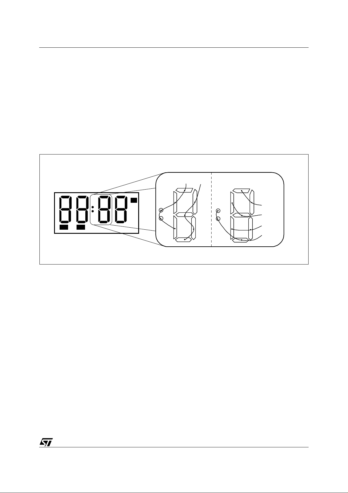
The targeted LCD is organized into four classical 7-segment digits, plus four icons (e.g. a
colon at the middle), creating four “8-segment digits”. Each digit uses the four backplane pins
and two frontplane pins.
Figure 6. Connections for an 8-segment digit (example with a colon)
S
3
2
COM
3
COM
2
COM
1
COM
0
AM PM
S
°C
Typically, this kind of LCD is suited to 24-hour c lock display. Therefore, the dig its are called,
from left to right: “hours digit 1”, “hours digit 0”, “minutes digit 1”, “minutes digit 0”.
The first part of this section explains how to use the library provided the LCD is wired exactly
like the target is, and provided the MCU pin allocations are compatible with the rest of the application. The second part give s m ore details on the data o perations pe rformed intern ally by
the driver, to be able to customise it if necessary. Finally, the thi rd part gives an example of
how to manage timing resources to combine LCD requirements with the main tasks of the application.
2.1 NON-CUSTOMISED USAGE
2.1.1 Allocation of I/O resources
S
All the MCU output pins generating the
signals are located in the same I/O port, cal led “seg-
ments port”. A diff eren t I/O po rt, c alle d “com mon s po rt” is u sed fo r the pi ns ge nera tin g the
COM
signals. The software driver has no effect on the other I/O pins, even if they are located
in one of those ports.
7/26

4-MULTIPLEXED LCD WITH A STANDARD ST62
The code uses DR_seg, DDR_seg and OR_seg labels to access the configuration registers of
the segments port. DR_com, DDR_com and OR_com labels are used for the commons port.
DR_seg_2 and DR_com_2 are labels referring to RAM variables used as shadow I/O port
Data Registers. The se 8 labe ls are decla red as e xterna l at t he beginning o f L CD_d rv.st6.
Therefore, to make the library work, y ou mus t define th em as sy nonyms o f actual configuration registers, like in the following example:
DDR_com DATA DDRB
DR_com DATA DRB
OR_com DATA ORB
DDR_seg DATA DDRA
DR_seg DATA DRA
OR_seg DATA ORA
DR_com_2 DATA DRB_2
DR_seg_2 DATA DRA_2
These definitions must be performed in another source file which is to be linked with
LCD_drv.st6.
Note: in this example, DRA_2 and DRB_2 definitions must be in the same source file as
DR_seg_2 and DR_com_2 definitions, otherwise the DATA directive does not wor k.
Once the segments and commons ports defined, the MCU must be wired according to Figure
6. Note that a pair of S pins is assigned to each “8-segment digit”. To understand the roles of
each of the two pins, refer to Figure 6.
8/26

4-MULTIPLEXED LCD WITH A STANDARD ST62
LCD
Figure 7. Template for MCU – LCD connectio ns
COM
COM
COM
COM
S
0
0
1
2
3
°C
AM
S
S
6
7
PM
S
S
S
S
5
S
3
4
1
2
Vdd
pin3 pin0 pin1 pin2 pin4 pin5 pin6 pin7
segments port
pin3
pin
pin
pin
2
1
0
ST62
commons
port
470k resistors
2.1.2 Driver subroutines and variables
The main application communicates with the LCD driver through six 8- bit variabl es and 3 s ubroutines, all declared in LCD_drv.inc.
The six variables are written by the main application and read by the softw are LCD driver.
They describe the information that should be displayed:
– hr_dig1, hr_dig0, min_dig1 and min_dig0 contain the code of the character to be di s-
played on each 7-segment digit;
– icons is a byte of flags indicating, for each icon, if it must be ON or OFF;
– flashing is a byte of flags indicating, for each 7-segment digit and each icon, if it must be
flashing or not.
9/26

4-MULTIPLEXED LCD WITH A STANDARD ST62
The driver supports 16 differen t characters to be displayed on a digit: the 10 numeri c digits,
some letters or symbols, or the blank digit. The character coding is included in the library
through a look-up table.
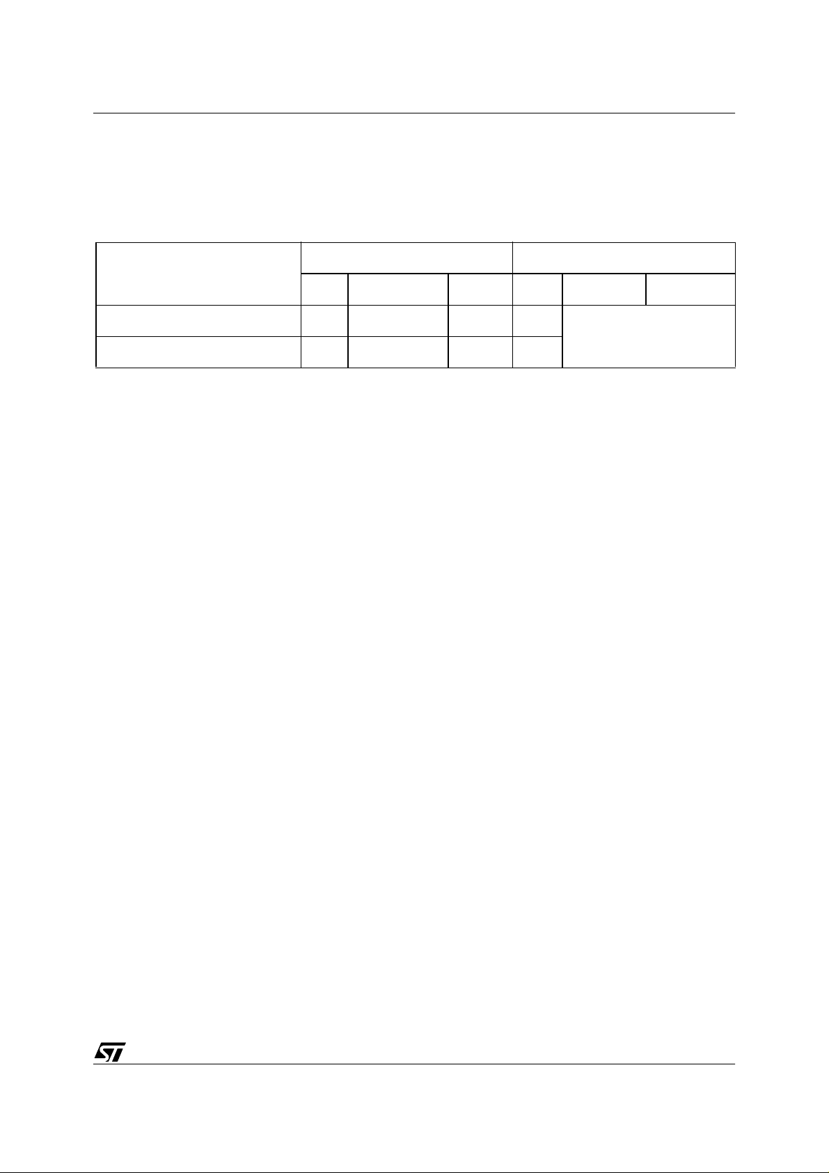
Table 2. Character coding for 7-segment digits
Code 0 1 2 3 4 5 6 7 8 9 a b c d e f
Display
Table 3 . Bit d efinitions for icons variab le
7 0
- - - - ICO3 ICO2 ICO1 ICO0
Bit 3:0 = ICO[3..0]
These bits indicate, for each icon segment, if it must be on or off.
0: Icon segment off
1: Icon segment on
Table 4 . Bit d efinitions for flashing variable
7 0
HR0 HR1 MIN0 MIN1 ICO3 ICO2 ICO1 ICO0
Bit 3:0 = ICO[3..0]
These bits indicate, for each icon segment, if it must be flashing or not.
0: Icon segment not flashing
1: Icon segment flashing
Bit 5:4 = MIN[1..0]
These bits indicate, for each minute 7-segment digit, if it must be flashing or not.
0: Digit not flashing
1: Digit flashing
Icon on/off
Icon flashing on/off
Minute digit flashing on/off
Bit 7:6 = HR[3..0]
These bits indicate, for each hour 7-segment digit, if it must be flashing or not.
0: Digit not flashing
1: Digit flashing
10/26
Hour digit flashing on/off

4-MULTIPLEXED LCD WITH A STANDARD ST62
To use the LCD driver, proceed as follows:
– Before calling any LCD driver subroutine, the main routine must initialise the six display var-
iables.
– Then, it must call the LCD_Init subroutine to initialise LCD driver internal variables and to
configure segment port pins as output push-pull.
– Once the LCD_Init subroutine called, the mai n softw are must frequently call the LCD_Do
subroutine. This subroutine updates the I/O ports so as to generate the required waveforms.
The delay between two consecutive calls to LCD_Do represents the duration of 1 LCD phase,
whic h is 1/8
th
of the total LCD cycle (cf. Section 1.3).
– The six display variables can be modified at any time by the main software. Each time the
LCD_Do subroutine is executed, it reports the changes on the waveforms, i.e. on the LCD.
– In parallel to LCD_Do calls, the main software must call the LCD_Flash subroutine. The de-
lay between two consecutive calls to LCD_Flash represents half of the flashing period.
– It is the main software that is in charge of generating a time base (generally using a timer
peripheral). This way, a single time base can be used at the same time for LCD driving, flash-
ing frequency and other application tasks.
Important notice: if delays between calls to LCD_Do are too irregular, LCD segment absolute
DC voltage can become too high, with a risk of damaging the LCD.
2.2 ADDITIONAL INFORMATION FOR CUSTOMISATION
The current LCD phase (ϕ
to ϕ7) is stored into LCD_Ph, an 8-bit variable internal to the LCD
0
driver. This variable is initialised by LCD_Init and incremented by LCD_Do , from 0 to 7 and
back to 0. To update the configuration register of the segments and commons ports, LCD_Do
uses LCD_Ph as an index to scan look-up tables.
Note: because computing the new register values takes time, LCD_Do stores the new values
in RAM buffers, and updates all the real registers at the same time. This way, transitions on
backplane and frontplane waveforms can be synchronised. This synchronisation helps
keeping a low DC voltage on LCD segments. For Data Registers, the RAM buffer used is the
shadow register.
The algorithms described in this section are designed to generate the proper backplane and
frontplane signals as described in Section 1.3.
2.2.1 Generation of backplane signals
Each time LCD_Do is executed, it updat es the thr ee configurati on regist ers (DDR, DR and OR)
V
/2 or
V
of the commons port, in order to output either 0,
DD
on the backplane pins.
DD
LCD_drv.st6 defines three co nstant tables giving the v alues o f each c onfiguration regi ster
depending on the current LCD phase:
11/26

4-MULTIPLEXED LCD WITH A STANDARD ST62
wave_ddr: DB 001h,002h,004h,008h,001h,002h,004h,008h
wave_dr: DB 00fh,00fh,00fh,00fh,00eh,00dh,00bh,007h
wave_or: DB 001h,002h,004h,008h,001h,002h,004h,008h
When applying these values to the port registers, LCD_Do uses a mask (COM_MASK equate) to
modify only the appropriate pins. To modify the Data Register, it uses DR_com_2 shadow register.
How to customise:
it is easy to modify the pins allocation for backplane pins, as long as they
all belong to the same I/O port. You only need to change COM_MASK and the three constant tables.
2.2.2 Generation of frontplane signals
Here, LCD_Do only has to upd ate the D ata Regist er. But operat ions a re mor e compl ex be-
cause of character coding.
The procedure contains four steps:
Step 1:
Writing into variables that are images of min_dig0, min_dig1, hr_dig0, hr_dig1
and icons, taking flashing into account : the image variable contains either a blank value or
the con tent of t he origi nal v ariabl e. This imag e varia ble repr esen ts wh at is rea lly to be dis-
played on the LCD. For example, if a digit displays a flashing “9”, its image variable contains
alternately '9' or 'f' (code for blank digit).
Step 2:
Updating the Data shadow Register only considering the 7-segment characters. This
requires a constant table to store character coding.
Step 3:
Step 4:
Steps 1 and 4
Updating the Data shadow Register taking the icons into account.
Copying the Data shadow Register into the Data Register.
are independent from I/O pins allocation, so they will not be described here.
Step 2
starts by clearing the Data shadow Register for all the frontplane pins. Then, for each
7-segment digit, the cycle of operations described by Figure 8 modifies this shadow register.
Due to the mask mec hanism, the ADD operation is equi valent to an O R ( the ST6 instruct ion
set does not supply a direct OR operation).
Because al l icon segm ents are locat ed on the fir st backpl ane (COM
only in phases ϕ
and ϕ4. After Step 2, the Data shadow Register is configured in a way that
0
0
Step 3
is performed
),
all icon segments are OFF. Step 3 consists in correcting the s hadow register to make sure that
all required icons are ON. To do this, it performs bit manipulation instructions with the following
bit definition equates:
ICON0_SEG EQU 1
ICON1_SEG EQU 3
ICON2_SEG EQU 5
ICON3_SEG EQU 7
12/26

4-MULTIPLEXED LCD WITH A STANDARD ST62
new value stored
up table defined
6
How to customise:
as long as all frontplane pins belong to the same I/O port, it is possible to
change I/O pin allocations or character coding just by modifying the equates and constant
table definitions located at the beginning of LCD_drv.st6:
– the mask equates selecting all or a subset of the frontplane pins,
– the look-up table for character coding,
– the bit definition equates selecting frontplane pins related to icon segments.
Figure 8. Operations to convert a character code in to a f rontplane waveform
Example with minutes dig it 1
LCD_Ph = 4
min_dig1 = 9
Step 1
min_dig1I = 9
image variable of
min_dig1
charac: DB 0aah,000h,055h,000h ; display 0
DB 0ffh,0aah,0ffh,0aah ; display 1
DB 0aah,055h,0aah,000h ; display 2
DB 0aah,0aah,0aah,000h ; display 3
DB 0ffh,0aah,000h,0aah ; display 4
DB 0aah,0aah,000h,055h ; display 5
DB 0aah,000h,000h,055h ; display 6
DB 0ffh,0aah,0ffh,000h ; display 7
DB 0aah,000h,000h,000h ; display 8
DB 0aah,0aah,000h,000h ; display 9
DB 0ffh,000h,000h,0aah ; display H
DB 0ffh,0ffh,0aah,0ffh ; display DB 0aah,055h,055h,0aah ; display L
DB 0ffh,055h,000h,000h ; display P
DB 0aah,055h,000h,055h ; display E
DB 0ffh,0ffh,0ffh,0ffh ; display ’Blank’
LCD_Ph mod 4 = 0
look-
in LCD_drv.st
equates defined in
1 1 1 0 0 0 1 0
LCD_drv.st6
; (Bit = 1) <=> pin is a frontplane pin for:
MIN0_SEL EQU 003h ; - digit 0 for minutes
MIN1_SEL EQU 00ch ; - digit 1 for minutes
HR0_SEL EQU 030h ; - digit 0 for hours
HR1_SEL EQU 0c0h ; - digit 1 for hours
0 0 1 0 1 0 0 0
previous value of
AND
DR_seg_2
0 0 0 0 0 1 0 0
0 0 1 0 0 0 0 0
ADD
0 0 1 0 0 1 0 0
LCD_Ph ≥ 4
inversion
1 1 1 0 0 0 1 0
into
DR_seg_2
13/26

4-MULTIPLEXED LCD WITH A STANDARD ST62
2.3 EXAMPLE OF APPLICATION TIMIN G – A SIMPLE CLOC K
As explained in Section 2.1, the main application is in charge of providing the time base to the
LCD driver. Because this time base must be relatively precise, it is usually generated by a specific sub- system of the a pplic ation , either in tern al to the MCU (timer p eriph eral) or exter nal
(e.g. external clock source, RC network, etc.). In both c ases, MCU resources are dedicated to
it (peripheral if internal, pins if external). This part describes a solution to share a single time
base between the LCD driver and the main application. Sharing is usually necessary if the
ST6 device has few resources.
The main application is a real time 24-hour clock to be displayed on the LCD. In order to use
as few pins as pos sible, the time base is gener ated b y a st andard 8-bit ti mer c locked by the
MCU internal clock.
The real time clock requires frequencies far lower than the LCD driver. Consequently, the time
base runs at the frequency required by the LCD driver. Then, this frequency is divided by software counters to reach a period of 125 ms, then divided again to reach periods of 0.5 second,
1 second, 1 minute and 1 hour. The half-second period is involved in making some LCD segments flash at 1 Hz. For example, when the clock is running, the colon flashes at that frequency.
The standard timer is configured in output mode with interrupts enabled, so that the timer Interrupt Service Routine (ISR) is called every 1.5 ms. This routine calls the LCD_Do routine. As
a result, a n LCD cycle (8 phas es) las ts 1.5* 8 = 1 2 ms, so LC D vol tage fr equenc y is 83 Hz,
which is in the required range.
Reaching a period of 125 m s requires dividing the timer interrupt frequenc y by 250/3. To do
so, the timer ISR decrements a counter (RAM variable) three times. After each decrement, it
checks if the counter has reached 0 or not. If i t has, the ISR calls an RTC subroutine. This subroutine reloads the counter with 250.
The RTC subroutine, called once every 1/8 s , pe rforms several frequency divisions to update
the second, minute and hour counters. Also, it calls LCD_Flash once every half second.
14/26

4-MULTIPLEXED LCD WITH A STANDARD ST62
3 APPENDI X: SOURCE CODE
LCD_drv.inc
; *********************************************************
;* (C) 2001 STMicroelectronics *
;* Project : 8*4 segment LCD software driver *
;* Toolchain : ST6 toolchain for RIDE V 1.0.C *
;* Target : in theory, any ST62 *
;* Module : LCD_drv.inc *
;* Version : V 0.1.1 - May 2001 *
;* Author : T.B. Hong Kong Application *
; *********************************************************
;* Software LCD driver library: *
;* - definitions of the variables *
;* - constant tables *
;* - driver subroutines *
; *********************************************************
;*-*-*-*-*-*-*-*-*-*-*-*-*-*-*-*-*-*-*-*-*-*-*-*
; *-*-*-*-*- Variables and Equates *-*-*-*-*-*;*-*-*-*-*-*-*-*-*-*-*-*-*-*-*-*-*-*-*-*-*-*-*-*
; Character codes
EXTERN DATA (min_dig0) ; Digit 0 for minutes
EXTERN DATA (min_dig1) ; Digit 1 for minutes
EXTERN DATA (hr_dig0) ; Digit 0 for hours
EXTERN DATA (hr_dig1) ; Digit 1 for hours
; Code : 0 1 2 3 4 5 6 7 8 9 a b c d e f
; Display : 0 1 2 3 4 5 6 7 8 9 H - L P E
BLANK EQU 0fh
DASH EQU 0bh
EXTERN DATA (icons) ; Byte of flags for icons on/off state
; (0 = off, 1 = on)
EXTERN DATA (flashing) ; Byte of flags for digits and icons
; flashing state
; (0 = not flashing, 1 = flashing)
; Bit definitions for ’icons’ and ’flashing’ variables
ICO0 EQU 0 ; bit 0: icon 0
ICO1 EQU 1 ; bit 1: icon 1
ICO2 EQU 2 ; bit 2: icon 2
ICO3 EQU 3 ; bit 3: icon 3
MIN0 EQU 4 ; bit 4: digit 0 for minutes
MIN1 EQU 5 ; bit 5: digit 1 for minutes
HR0 EQU 6 ; bit 6: digit 0 for hours
HR1 EQU 7 ; bit 7: digit 1 for hours
15/26

4-MULTIPLEXED LCD WITH A STANDARD ST62
;*-*-*-*-*-*-*-*-*-*-*-*-*-*-*-*-*-*-*-*-*-*-*-*
; *-*-*-*-*-*-*-* Subroutines *-*-*-*-*-*-*-*-*
;*-*-*-*-*-*-*-*-*-*-*-*-*-*-*-*-*-*-*-*-*-*-*-*
;*****************************************************************
EXTERN CODE (LCD_Init)
; Initialises the ressources used by the library.
; Prereq. : none
; Inputs : none
; Outputs : internal variables initialised,
; segment pins configured as output push-pull
;*****************************************************************
;*****************************************************************
EXTERN CODE (LCD_Flash)
; Switches the flash strobe if necessary
; Prereq. : none
; Inputs : flashing
; Outputs : none
;*****************************************************************
;*****************************************************************
EXTERN CODE (LCD_Do)
; Updates the LCD outputs (commons & segments) to
; display the requested digits.
; Prereq. : ’LCD_Init’ called before
; Inputs : ’min_dig0’, ’min_dig1’, ’hr_dig0’, ’hr_dig1’
;+ ’icons’
; Outputs : ’DDR_com’, ’DR_com’, ’DR_com_2’, ’OR_com’,
; ’DR_seg’ and ’DR_seg_2’ refreshed
; IMPORTANT: once the LCD I/Os are initialised, this
; subroutine must be called frequently to prevent
; damaging the LCD.
;*****************************************************************
;******************* (C) 2001 STMicroelectronics *****************
16/26

4-MULTIPLEXED LCD WITH A STANDARD ST62
LCD_drv.st6
; *********************************************************
;* (C) 2001 STMicroelectronics *
;* Project : 8*4 segment LCD software driver *
;* Toolchain : ST6 toolchain for RIDE V 1.0.C *
;* Target : in theory, any ST62 *
;* Module : LCD_drv.st6 *
;* Version : V 0.1.2 - June 2001 *
;* Author : T.B. Hong Kong Application *
; *********************************************************
;* Software LCD driver library: *
;* - public and local variables *
;* - constant tables *
;* - driver subroutines *
; *********************************************************
$INCLUDE (LCD_drv.inc) ; Software LCD driver
;*-*-*-*-*-*-*-*-*-*-*-*-*-*-*-*-*-*-*-*-*-*-*-*
; *-*-*-*-*- I/O configuration equates *-*-*-*;*-*-*-*-*-*-*-*-*-*-*-*-*-*-*-*-*-*-*-*-*-*-*-*
; --- Port allocation ---
EXTERN DATA (DDR_com, DR_com, OR_com) ; LCD commons
EXTERN DATA (DDR_seg, DR_seg, OR_seg) ; LCD segments
EXTERN DATA (DR_com_2, DR_seg_2) ; LCD shadow registers
; --- Pin allocation ---
COM_MASK EQU 0f0h
SEG_MASK EQU 000h
SEG_SEL EQU 0ffh
MIN0_SEL EQU 003h
MIN1_SEL EQU 00ch
HR0_SEL EQU 030h
HR1_SEL EQU 0c0h
ICON0_SEG EQU 1
ICON1_SEG EQU 3
ICON2_SEG EQU 5
ICON3_SEG EQU 7
17/26

4-MULTIPLEXED LCD WITH A STANDARD ST62
;*-*-*-*-*-*-*-*-*-*-*-*-*-*-*-*-*-*-*-*-*-*-*-*
; *-*-*-*-*-*-*-*- Variables *-*-*-*-*-*-*-*-*;*-*-*-*-*-*-*-*-*-*-*-*-*-*-*-*-*-*-*-*-*-*-*-*
LCD_vars SEGMENT DATA
RSEG LCD_vars
;--- Public variables ---
PUBLIC min_dig0, min_dig1, hr_dig0, hr_dig1
PUBLIC icons, flashing
; Character codes
min_dig0: DS 1 ; Digit 0 for minutes
min_dig1: DS 1 ; Digit 1 for minutes
hr_dig0: DS 1 ; Digit 0 for hours
hr_dig1: DS 1 ; Digit 1 for hours
; Code : 0 1 2 3 4 5 6 7 8 9 a b c d e f
; Display : 0 1 2 3 4 5 6 7 8 9 H - L P E
icons: DS 1 ; Byte of flags for icons on/off state
; (0 = off, 1 = on)
flashing: DS 1 ; Byte of flags for digits and icons
; flashing state
; (0 = not flashing, 1 = flashing)
;--- Local variables ---
LCD_Ph: DS 1 ; LCD phase (0 to 7)
DDR_com2: DS 1
OR_com2: DS 1
strobe: DS 1 ; Flash strobe (000h <--> 0ffh)
mindig0I: DS 1 ; Digit 0 for minutes - IMAGE
mindig1I: DS 1 ; Digit 1 for minutes - IMAGE
hrdig0I: DS 1 ; Digit 0 for hours - IMAGE
hrdig1I: DS 1 ; Digit 1 for hours - IMAGE
iconsI: DS 1 ; Icons - IMAGE
18/26

4-MULTIPLEXED LCD WITH A STANDARD ST62
;*-*-*-*-*-*-*-*-*-*-*-*-*-*-*-*-*-*-*-*-*-*-*-*
; *-*-*-*-*-*-* Constant tables *-*-*-*-*-*-*-*
;*-*-*-*-*-*-*-*-*-*-*-*-*-*-*-*-*-*-*-*-*-*-*-*
; Table of common I/Os configuration for commons waveform
Com_table SEGMENT CODE INWINDOW
RSEG Com_table
; phase | 0 1 2 3 4 5 6 7
;----------------------------------------------------------------------; COM0 | Vdd Vdd/2 Vdd/2 Vdd/2 0 Vdd/2 Vdd/2 Vdd/2
; COM1 | Vdd/2 Vdd Vdd/2 Vdd/2 Vdd/2 0 Vdd/2 Vdd/2
; COM2 | Vdd/2 Vdd/2 Vdd Vdd/2 Vdd/2 Vdd/2 0 Vdd/2
; COM3 | Vdd/2 Vdd/2 Vdd/2 Vdd Vdd/2 Vdd/2 Vdd/2 0
wave_ddr: DB 001h,002h,004h,008h,001h,002h,004h,008h
wave_dr: DB 00fh,00fh,00fh,00fh,00eh,00dh,00bh,007h
wave_or: DB 001h,002h,004h,008h,001h,002h,004h,008h
; Table of segment outputs to display a specific character
Seg_table SEGMENT CODE INWINDOW
RSEG Seg_table
charac: DB 0aah,000h,055h,000h ; display 0
DB 0ffh,0aah,0ffh,0aah ; display 1
DB 0aah,055h,0aah,000h ; display 2
DB 0aah,0aah,0aah,000h ; display 3
DB 0ffh,0aah,000h,0aah ; display 4
DB 0aah,0aah,000h,055h ; display 5
DB 0aah,000h,000h,055h ; display 6
DB 0ffh,0aah,0ffh,000h ; display 7
DB 0aah,000h,000h,000h ; display 8
DB 0aah,0aah,000h,000h ; display 9
DB 0ffh,000h,000h,0aah ; display H
DB 0ffh,0ffh,0aah,0ffh ; display DB 0aah,055h,055h,0aah ; display L
DB 0ffh,055h,000h,000h ; display P
DB 0aah,055h,000h,055h ; display E
DB 0ffh,0ffh,0ffh,0ffh ; display ’Blank’
19/26

4-MULTIPLEXED LCD WITH A STANDARD ST62
;*-*-*-*-*-*-*-*-*-*-*-*-*-*-*-*-*-*-*-*-*-*-*-*
; *-*-*-*-*-*-*-* Subroutines *-*-*-*-*-*-*-*-*
;*-*-*-*-*-*-*-*-*-*-*-*-*-*-*-*-*-*-*-*-*-*-*-*
PUBLIC LCD_Init, LCD_Flash, LCD_Do
LCD_subs SEGMENT CODE
RSEG LCD_subs
;*****************************************************************
LCD_Init: ; Initialises the ressources used by the library.
; Prereq. : display variables must have been initialised
; by the main routine
; Inputs : none
; Outputs : internal variables initialised,
; segment pins configured as output push-pull
;*****************************************************************
clr LCD_Ph
clr strobe
ldi a,SEG_SEL
add a,DDR_seg
ld DDR_seg,a
ldi a,SEG_SEL
add a,OR_seg
ld OR_seg,a
; Output internal to the driver:
; ’LCD_Ph’ and ’strobe’ initialised’
ret
;*****************************************************************
LCD_Flash: ; Switches the flash strobe if necessary
; Prereq. : none
; Inputs : ’flashing’
; Outputs : none
;*****************************************************************
ld a,strobe
jrnz strobe1
strobe0: ld a,flashing
jrz exit_sub
ldi strobe,0ffh
exit_sub: ret
strobe1: clr strobe
ret
20/26

4-MULTIPLEXED LCD WITH A STANDARD ST62
;*****************************************************************
LCD_Do: ; Updates the LCD outputs (commons & segments) to
; display the requested digits.
; Prereq. : ’LCD_Init’ called before
; Inputs : ’min_dig0’, ’min_dig1’, ’hr_dig0’, ’hr_dig1’
; + ’icons’
; Outputs : ’DDR_com’, ’DR_com’, ’DR_com_2’, ’OR_com’,
; ’DR_seg’ and ’DR_seg_2’ refreshed
; IMPORTANT: once the LCD I/Os are initialised, this
; subroutine must be called frequently to prevent
; damaging the LCD.
;*****************************************************************
;--- Depending on flash strobe, update segment images ---
ld a,min_dig0
jrr 0,strobe,min0
jrr MIN0,flashing,min0
ldi a,BLANK
min0: ld mindig0I,a
ld a,min_dig1
jrr 0,strobe,min1
jrr MIN1,flashing,min1
ldi a,BLANK
min1: ld mindig1I,a
ld a,hr_dig0
jrr 0,strobe,hr0
jrr HR0,flashing,hr0
ldi a,BLANK
hr0: ld hrdig0I,a
ld a,hr_dig1
jrr 0,strobe,hr1
jrr HR1,flashing,hr1
ldi a,BLANK
hr1: ld hrdig1I,a
clr a
jrr 0,strobe,iconsegs
ld a,flashing
iconsegs: com a
and a,icons
ld iconsI,a
21/26

4-MULTIPLEXED LCD WITH A STANDARD ST62
;--- Update segments outputs (shadow register) ---
seg_upd: ld a,DR_seg_2
andi a,SEG_MASK
ld DR_seg_2,a
ld a,LCD_Ph
andi a,03h
ld V,a ; v = LCD_Ph mod 4
; -- Numeric digits --
; Digit 0 for minutes
ld a,mindig0I
ldi W,MIN0_SEL
call find_seg
; Digit 1 for minutes
ld a,mindig1I
ldi W,MIN1_SEL
call find_seg
; Digit 0 for hours
ld a,hrdig0I
ldi W,HR0_SEL
call find_seg
; Digit 1 for hours
ld a,hrdig1I
ldi W,HR1_SEL
call find_seg
; -- Icons --
ld a,V
jrz do_icon0 ; All icon segments are on COM0
jp com_upd
; icon 0 segment
do_icon0: jrr ICO0,iconsI,do_icon1
jrs 2,LCD_Ph,icon0_1
icon0_0: res ICON0_SEG,DR_seg_2
jp do_icon1
icon0_1: set ICON0_SEG,DR_seg_2
22/26

4-MULTIPLEXED LCD WITH A STANDARD ST62
; icon 1 segment
do_icon1: jrr ICO1,iconsI,do_icon2
jrs 2,LCD_Ph,icon1_1
icon1_0: res ICON1_SEG,DR_seg_2
jp do_icon2
icon1_1: set ICON1_SEG,DR_seg_2
; icon 2 segment
do_icon2: jrr ICO2,iconsI,do_icon3
jrs 2,LCD_Ph,icon2_1
icon2_0: res ICON2_SEG,DR_seg_2
jp do_icon3
icon2_1: set ICON2_SEG,DR_seg_2
; icon 3 segment
do_icon3: jrr ICO3,iconsI,com_upd
jrs 2,LCD_Ph,icon3_1
icon3_0: res ICON3_SEG,DR_seg_2
jp com_upd
icon3_1: set ICON3_SEG,DR_seg_2
;--- Update commons I/Os (shadow registers) ---
com_upd: ldi DWR,#WINDOW(wave_ddr)
; Update DDR
ldi a,#WINOFFSET(wave_ddr)
add a,LCD_Ph
ld x,a
ld a,DDR_com
andi a,COM_MASK
add a,(x)
ld DDR_com2,a
; Update DR and DR_2
ldi a,#WINOFFSET(wave_dr)
add a,LCD_Ph
ld x,a
ld a,DR_com_2
andi a,COM_MASK
add a,(x)
ld DR_com_2,a
; Update OR
ldi a,#WINOFFSET(wave_or)
23/26

4-MULTIPLEXED LCD WITH A STANDARD ST62
add a,LCD_Ph
ld x,a
ld a,OR_com
andi a,COM_MASK
add a,(x)
ld OR_com2,a
;--- Perform the changes on the real ports ---
; Segments port
ld a,DR_seg_2
ld DR_seg,a
; Commons port
ld a,OR_com
andi a,COM_MASK
ld OR_com,a
ld a,DDR_com2
ld DDR_com,a
ld a,DR_com_2
ld DR_com,a
ld a,OR_com2
ld OR_com,a
;--- Increment phase counter ---
inc LCD_Ph
ld a,LCD_Ph
andi a,07h
ld LCD_Ph,a ; LCD_Ph = (LCD_Ph + 1) mod 8
; Output internal to the driver:
; ’LCD_Ph’ updated
ret
;*****************************************************************
find_seg: ; Finds the segment outputs for a given digit, a given
; character and a given LCD phase.
; Prereq. : none
; Inputs : ’LCD_Ph’, V = LCD_Ph mod 4,
; a = code of the character (0 to 15),
; W = segment I/O port mask for the digit
; Outputs : ’DR_seg_2’ refreshed
; Modifies : X
;*****************************************************************
24/26

sla a
sla a ; * 4
ldi DWR,#WINDOW(charac)
addi a,#WINOFFSET(charac)
add a,V
ld x,a
ld a,(x)
jrr 2,LCD_Ph, dr_chg ; If LCD_Ph >= 4,
com a ; invert outputs
dr_chg: and a,W
add a,DR_seg_2
ld DR_seg_2,a
ret
END
4-MULTIPLEXED LCD WITH A STANDARD ST62
;******************* (C) 2001 STMicroelectronics *****************
25/26

4-MULTIPLEXED LCD WITH A STANDARD ST62
"THE PRESENT NOTE WHICH IS FOR GUIDANCE ONLY AIMS AT PROVIDING CUSTOMERS WITH INFORMATION REGARDING THEIR PRODUCTS IN ORDER FOR THEM
TO SAVE T IME. AS A R ESU L T, S TM ICROE LEC TR ON ICS SHA LL NOT BE H E LD L IAB LE
FOR ANY DIRECT, INDIRECT OR CONSEQUENTIAL DAMAGES WITH RESPECT TO ANY
CLAIMS ARISING FROM THE CONTENT OF SUCH A NOTE AND/OR THE USE MADE BY
CUSTOMERS OF THE INFORMATION CONTAINED HEREIN IN CONNEXION WITH
THEIR PRODUCTS."
Information furnished is believed to be accurate and reliable. However, STMicroelectronics assumes no responsibility for the consequences
of use of such information nor for any infringement of patents or other rights of third parties which may result from its use. No license is granted
by implic ation or otherwise under any patent or patent ri ghts of STM i croelectr oni cs. Specifications mentioned in thi s publicati on are subject
to change without notice. This publication supersedes and replaces all information previously supplied. STMicroelectronics products are not
authorized for use as cri tical comp onents in life support dev i ces or systems wi thout the express written approv al of STMicroel e ctronics.
The ST logo is a registered trademark of STMicroelectronics
2001 STMicroelectronics - All Rights Reserved.
Purchase of I
Australi a - Brazil - China - Finland - France - Germany - Hong Kong - India - Italy - Japan - Malaysia - Malt a - Morocco - Singapore - Spain
2
C Components by STMicroelectronics conveys a license under the Philips I2C Patent. Rights to use the se components in an
2
I
C system i s granted pro vid ed that the sy stem conforms to the I2C Standard Specification as defined by Philips.
STMicroelectronics Group of Compan i es
Sweden - Switzerland - United K i ngdom - U.S. A.
http://www.s t. com
26/26
 Loading...