

Page 1

AN1387
APPLICATION NOTE
APPL ICATION OF A NEW MON OL IT HI C SM ART IG BT
IN DC MOTOR CONTROL FOR HOME APPLIANCES
A. Alessandria - L. Fragapane - S. Musumeci
1. ABSTRACT
This application notes aims to outline the characteristics of a new power device that joins the peculiarities
of an STMicroelectronics fast-switching PowerMESH™ IGBT with some novel protection features. A
driver circuit is integrated in the power device to implement over-current protection and soft thermal
shutdown. The current limitation also ensures a highly short-circuit rated device. Moreover the low
threshold voltage and inp ut current make it p ossible to drive the device directly from the output pin of a
microprocessor. The static and dynamic behavio r of the device will be illustrated and an applic ation will
be suggested.
2. INTRODUCTION.
In the last few yea rs IGB Ts have been appreciated in many appl ications in t he m id -power range, having
the advantage of bipolar conduction characteristics and insulated gate control. Efficient advances in
process and device technologies have improved conduction losses, working frequencies and
ruggedness under inductive load co nditions in hard switching applications. But nowada ys requirements
are becoming more and more stringent regarding ruggedness and reliability. On the other hand, the
planar technology is reaching its limit in terms of performance [1]. For this reason the monolithic
integration of protection features to prevent the intervention of faulty conditions represents a wi nning
choice in order to improve a device’s limits. Therefore the new trend in power semiconductor
manufacturers is to provide "system-on-chip" solutions [2].
Current literature proposes several sol utions in order to obtain an intelligent s witch in power conv ersion
applications, such as full-protected high voltage MOSFETs or IGBTs for automotive electronic ignition
[3,4]. But these solutions are not suitable for those applications in which conduction losses and switching
speed are both important. Indeed a Power MOSFET is good for high frequency applications, but at lower
current, while at the present time Smart IGB Ts are available only for low frequency applications, and the
research activities in the field of monolithic Smart IGBTs for fast-switching applications are really poor.
Hybrid solutions are actually available, but this approach has some drawbacks like package size,
complex assembly techniques and costs.
The device we are going to present (see figure 1) is very innovative in its product range, bec ause it
shows a high current density with switching performances that match well with the requirements of
applications like motor control drive systems, induction heating and SMPS.
November 2001
1/10
Page 2
AN1387 - APPLICATION NOTE
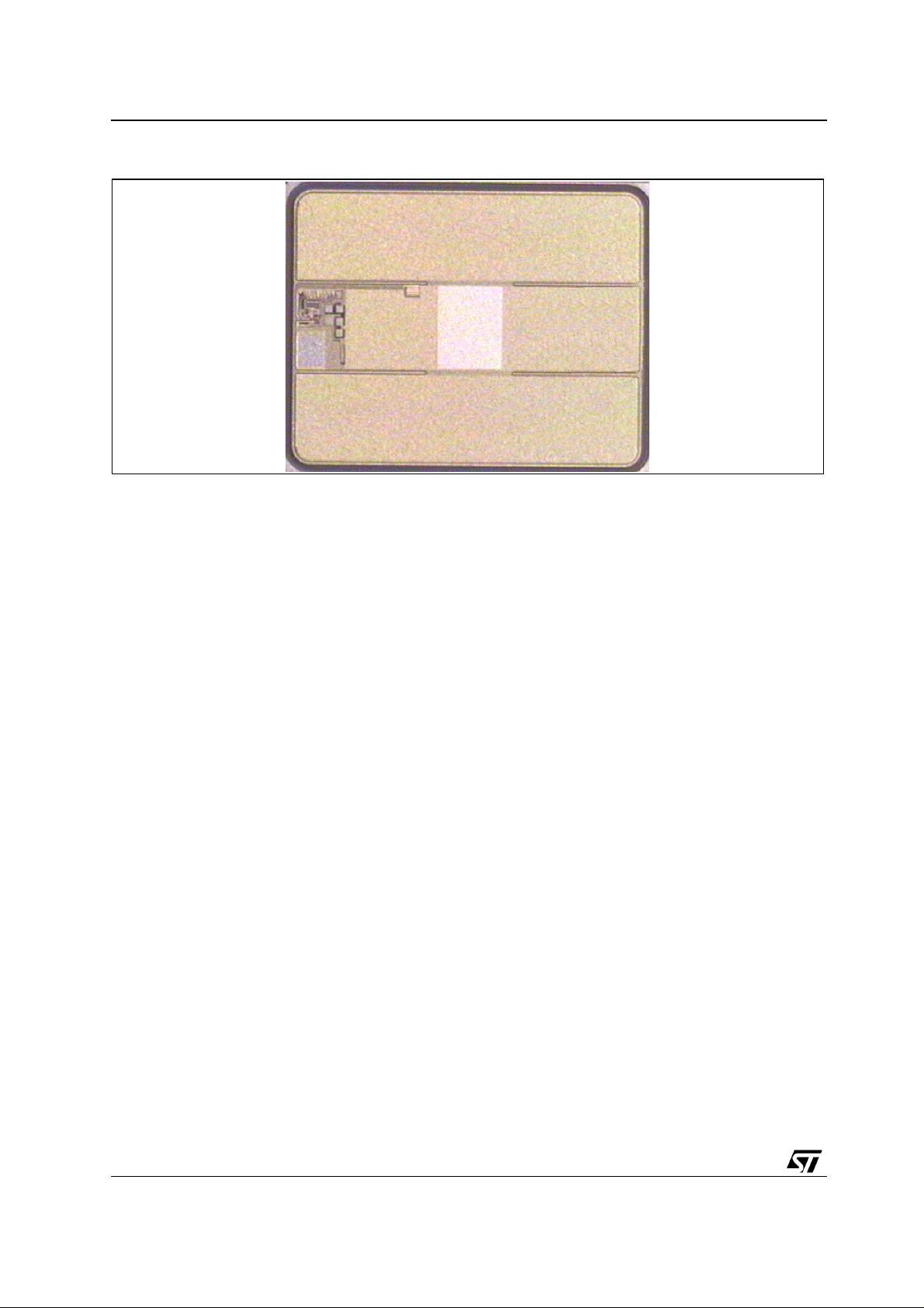
Figure 1: A Fast-Switching Smart IGBT
The proposed device is a new full-protec ted IG B T, packaged in a convenient three pin TO-220 package,
2
with an active area of about 12mm
, while the cont rol part occupi es an area of about 0.9mm2, including
the input pad and some trimming pads. Concerning the main electrical characteristics, the device has
600V of breakdown voltage and 10A of nomina l current. It is a logic level switch with a gate threshold
voltage of 1.5V and very low input current (1mA). These features allow direct driving from a micro
controller system. In this way STMicroelectronics’ intelligent switch is particularly suitable for motor
control in home appliances, consumer electronics and me dium power industri al servo-drive [5].
This paper will begin by giving some general information about the adopted technology and the static
and dynamic electrical characteristics of the device will then follow. In this context the dynamic
performances will be compared with the requirements of an experimental motor control application.
3. TECHNOLOGICAL OVERVIEW.
STMicroelectronics’ fast-switching Smart IGBT is manufac tured with a standard process based on its
patented strip horizontal layout. This layout consists of a p-type mesh implanted over an n-type epytaxial
layer. Some steps later n-type strips are then implanted over the p mesh to form the IGBT emitter. In
figure 2 the 3D view of the mesh layout is depicted, while in figure 3 the cross section of the strip layout
is shown.
2/10
Page 3
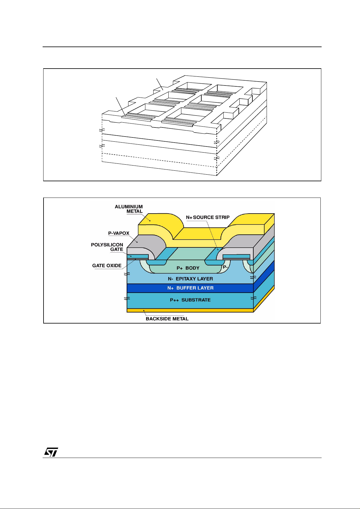
Figure 2: Mesh Overlay 3D View
N+ SOURC E
N
N
+
B
P
+
S
B
A
C
Figure 3: Strip Layout Cross Section
P EDGE
P
M
E
S
-
D
R
A
U
F
F
E
R
L
U
B
S
T
K
M
E
AN1387 - APPLICATION NOTE
H
I
N
A
Y
E
R
R
A
T
E
T
A
L
This proprietary process improves switching performances and latch-up immunity, moreover the
introduction of gate fingers concur to reduce the gate internal resistance and to speed-up the device turn
off [6]. Furthermore a proprietary lifetime killing m ethod is performed implanting and diffusing platinum
ions.
The technology desi gn al lows to integrate in the same c hi p the Power IGBT and a s imple c ontrol ci rcuit.
This approach ensures a low-cost integration and a high value-added device, indeed only one
photolithography process is added to the standard process flow.
The control circuit is implemented with:
• N-MOS enhancement-mode transistor,
• polysilicon resist or s,
• polysilicon diodes.
The sign al MOSFET tra nsistors are im planted in the p -type mesh, whi le the polysilic on resistors an d
3/10
Page 4

AN1387 - APPLICATION NOTE
diodes are insulated from the bulk by a thick field oxide.
Moreover a current sensor and a temperature sensor are integrated. Current sensing is made by
insulating an emitter strip with a given sens e ratio, while temperature s ensin g is m ade by monitoring the
variation of the forward voltage drop of some polysilicon diodes.
4. THE DEVICE: STATIC AND DYNAMIC BEHAVIOR.
The Smart IGBT has to be considered as a global switching system. The block diagram of the device is
shown in figure 4 where all the control parts are highlighted.
Figure 4: Block Diagram of the Smart IGBT For Motor Control
C
TEMPERATURE
SENSING
IGBT
SENSE
DRIVER
CIRCUIT
IGBT
MAIN
IN
VOLTAGE
REFERENCE
OVERTEMP.
PROTECTION
OVERCURRENT
PROTECTION
R
SENSE
GND
Although the exterior look of th e device is very similar to a standard IGB T of t he same silicon area (they
are both housed in a three pin package), the ir electrical characteristics are slightly different due to the
intervention of the devoted control circuit. The first difference of the Smart IGBT, with regard to a
standard IGBT, is the input current. The gate pin of an IGBT is an insulated terminal, while the input pin
of the Smart IGBT needs an input current of about 1mA at V
The threshold voltage of t he device is very low (1.5V @ I
consider the device on and correctly working is about 4V.
The output characteristics at high curren t are modified from the presence of the current limiter. In the
knee region of the characteristics we can note an abrupt reduction in the collector saturation current due
to the intervention of the current limiter (see figure 5). Moreover, the transconductance of the device is
smaller with respect to a standard IGBT due to the voltage drop in the control circuit.
=5V in the steady state conditions.
IN
=250µA), but t he minimum input v oltage to
C
The nominal current of the device is about 10A (current dens ity about 100A/cm
2
), at wh ich value the
collector saturation voltage is about 2.5V. In future releases of the device this characteristic will be
improved using further technological approaches.
4/10
Page 5

Figure 5: Smart IGBT Output Characteristics
[
]
20
18
16
14
12
A
10
Ic
8
6
4
2
0
012345678910
AN1387 - APPLICATION NOTE
Vce [V]
The current limitation shows a slight dependence on the value of the supply voltage and, in the
application suggested in th is paper, it starts at about 24A. The presence of the current limitation ensures
a good immunity to several faulty conditions. For example, if a short circuit occurs under switching
conditions, the collector current will be blocked at low values, several amperes below the latching
current, so the device will withstand short-circuit and its immunity is limited only by the capability of the
silicon chip to dissipate energy. In figure 6 a hard switching phase in short-circuit condition is shown. It is
easy to understand that the device does not fail for a very long period during which an external diagnostic
circuit could reveal the faulty condition and disable the input signal.
Figure 6: Ha rd S wi tc hi ng Sh ort C irc ui t Conditions (V
=50V/div, IC=5A/div, VIN=5V/div)
CE
Vce
Ic
Vin
<0
time [10 µs/div]
5/10
Page 6

AN1387 - APPLICATION NOTE
In figure 7 the initial phase of a sof t thermal shutdown due to the intervention of the over-temperat ure
protection circuit is shown. In the worst driving conditions, for example an error occurring in the
frequency or in the duty cycle of the timing train of pulses, the integrated control circuit will sense the high
temperature and will reduce the value of the collector current under limitation conditions.
Figure 7: Overtemperature Protecti on (I
=10A/div, VIN=10V/div, t=1ms/div)
C
IN
V
0>
C
I
0>
Time [1 ms/div]
With regards to switching times the device shows a current fall time of about 120ns, including current tail,
and a voltage rise t ime of about 150ns at room t em perat ure. In figure 9 a typical turn-off of the dev ice is
shown.
Figure 8: Inductive Turn-Off (V
0>
0>
6/10
=100V, IC=5A/div, VIN=5V/div, t=200ns)
CE
IN
V
C
I
Time [200 ns/div]
V
CE
Page 7

AN1387 - APPLICATION NOTE
5. DC MOTOR CONTROL: AN APPLICATION CASE.
Variable speed drives have become widespread in the home appliance field and the electrical
characteristics of the Smart IGBT make it suitable for motor control applications. In this field of
application the Smart IGBT allows a dramatic reduction in the probability of electrical block, improving the
system reliability. Furthermore the integration of the control circuit allows eliminating many external
components, resulting in cost and volume reduction.
We propose an application of the device as a power switch in a chopper c onvert er for a hom e appliance
DC motor of 400W. The system arrangements with a standard IGBT and with a Smart IGBT are
compared in figure 9. The diagram shows how the device is driven directly from the control circuit without
a driver and any protection circuitry . In order to improve the system reliability in short circuit condition, the
information of V
behavior has bee n supplied to MCU unit by means of a desaturation detection
CEsat
circuit.
Figure 9: A Comparison Of A Motor Control Application Circuit With a Smart IGBT and a Standard
IGBT
V
USER
INTERFACE
main
MCU
PWM
CONTROLLER
SUPPLY
5V
DESATURATION
DETECTOR
SMART
IGBT
OVER
TEMP
M
USER
INTERFACE
V
main
CONTROLLER
OVER VOLTAGE
DETECTOR
MCU
PWM
SUPPLY
15V-5V
DRIVING CIRCUIT
PEAK CURRENT
DETECTOR
OVER TEMPERATURE
DETECTOR
++
M
Several tests have been carried out at different switching frequency (in the range from 10kHz to 20kHz).
In figure 10 the transient phase of the motor starting at a switching frequency fixed at 10kHz is shown;
the supply voltage is 311V and the duty cycle is 50%. In this application the maximum collector current
reaches about 4A while at steady state it reduces to about 2.3A.
A load variation during the steady state conditions is reported in figure 11. The output current both
decrease and rise from light load to full load as simulation of discontinuous load applications.
In figure 12 the intervention of the over tempera ture protection is shown. The current has been strongly
reduced with consequen t temperature decreasing. The over temperature condit ion has been obtained
without heat sink. The temperature measured in the application is about 80°C corresponding at 100°C on
the junction.
7/10
Page 8

AN1387 - APPLICATION NOTE
Figure 10: Motor Control Starting Transient (VCE=100V/div, IC=2A/div, t=5ms)
Figure 11: Load Variation Transient (V
=100V/div, IC=1A/div, t=500ms)
CE
8/10
Page 9

AN1387 - APPLICATION NOTE
Figure 12: Overtemperature Current Reduction (IC=0.5A/div, t=100ms)
6. CONCLUSION.
A new fast smart IGBT with a monolithic control circuit has been presented and described. The device is
cost-effective because, while it has been manufactured with the same process of a standard IGBT, it
offers a great deal of added v alue. All the protection f eatures of the switch hav e been exploited; it was
also shown how they improve the reliability and the ruggedness of the whole system. Moreover a
switching performance of the device in a home appliance motor control application has been show n.
REFERENCES:
[1] Y. Onishi et al., ”Analysis On Device Structures For Next Generation IGBTs”. Procee dings of 1998
ISPSD.
[2] Y. Seki et al., “A New IGBT With A Monolithic Over Current Protection”. Proceedings of 1995 ISPSD.
[3] A. Alosi et al., “A New IGBT With A Monolithic Self-protection Circuit”. EPE 1997.
[4] Z.J. Shen, S.P. Robb, “A New Intelligent IGBT With A Monolithic Over Current and Over Temperature
Self-protection Circuit”. Proceedings of 1996 PCIM.
[5] A. Alessandria et al. “A new monolithic smart IGBT for motor control application”. Proceedings of
2001 EPE.
[6] A. Torres et al., ”A Fully Protected Mo nolithic Smart IGBT Developed With A Standard Technology”.
Proceedings of 1999 PCIM.
9/10
Page 10

AN1387 - APPLICATION NOTE
Information furnished is b elieved to be accurate a nd reliable. Howe ver, ST Microelectronics a ssumes no resp onsibility
for the consequences of use of such information nor for any infringement of patents or other rights of third parties
which may result from its use. No license is granted by implication or otherwise under any patent or patent rights of
STMicroelectronics. Specification ment ioned in this p ublication are subject to change without notice. This pub lica tion
supersedes and repla ces a ll information pre viously su pplied. STM icr oelectro nics pr oducts are not authorized for use
as critical components in life support devices or systems without express written approval of STMicroelectronics.
The ST logo is a registered trademark of STMicroelectronics
© 2001 STMicroelectronics - Printed in Italy - All rights reserved
Australia - Brazil - China - Finland - France - Germany - Hong Kong - India - Italy - Japan - Malaysia - Malta - Morocco -
Singapore - Spain - Sweden - Switzerland - United Kingdom - U.S.A.
10/10
STMicroelectronics GROUP OF COMPANIES
http://www.st.com
 Loading...