

Page 1
AN1379
Application note
Z01 and ACS behavior compared under fast voltage transients
Introduction
Home appliances such as washing machines, refrigerators and dishwashers integrate a lot
of low power loads such as valves, door lock systems, dispensers and drain pumps. These
loads are mains-powered in on / off mode, and are mostly controlled by Triacs or relays.
In most cases, the AC switching function now needs to be directly driven by a
microcontroller unit (MCU) and it must withstand the AC line transients to make the system
compliant with the new European Electromagnetic Compatibility (EMC) standards.
STMicroelectronics ACS™ (alternating current switches) have been designed to meet these
needs, as shown in this application note. Compared to Triacs, they offer high robustness and
dV/dt capability, while contributing to a substantial reduction of the overall electronic board
size.
The application specific discrete (ASD) concept, developed by STMicroelectronics, allows
several devices, such as diodes, thyristors, transistors and some passive components used
to make a complete function, to be integrated on the same silicon die. This technology has
been used to develop the new ACS structures.
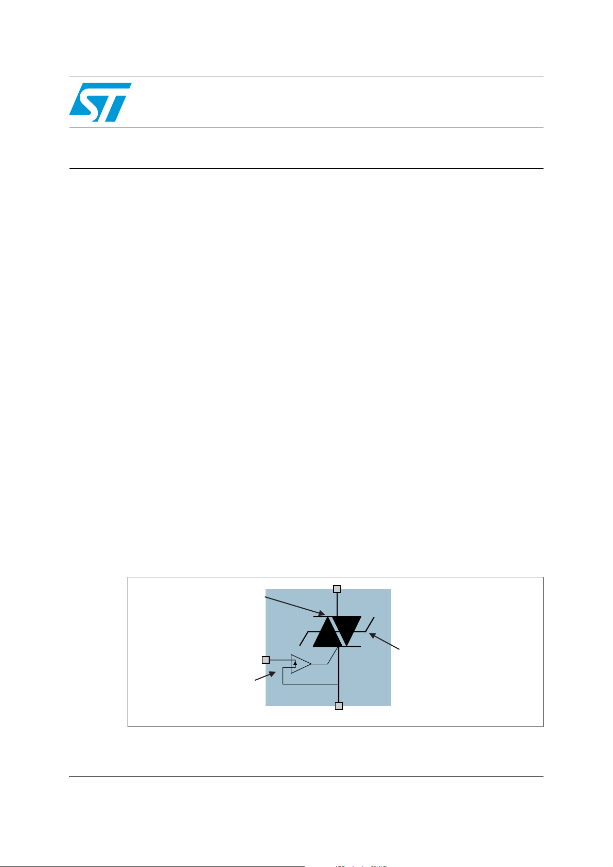
An ACS embeds an integrated driver, a clamping structure, and a bidirectional, thyristor-type
switch (see Figure 1). The primary loads to be targeted by these new devices are high
inductive loads like electromagnets, where the serial inductance can reach teens of Henry
and the turn-off operation can thus cause many problems. The second section explains how
the clamping feature of ACSs enables them to directly drive any inductive load without any
external clamping device, such as metal oxide varistors, and how ACSs can also sustain
overvoltages coming from the mains.
Silicon devices are subjected not only to surge voltages but also to fast transient voltages,
as described in the IEC 61000-4-4 standard. They must not only present clamping ability but
also high immunity to high dV/dt rates. The results of tests reported in this application note
show the maximum levels withstood by ACSs and Triacs, for different gate sensitivities.
Figure 1. ACS symbol description
AC power
switch
G
Integrated
driver
TM: Trisil is a trademark of STMicroelectronics
OUT
Over voltage
protection
(Trisil™ -Like)
COM
TM: ACS is a trademark of STMicroelectronics
June 2010 Doc ID 8317 Rev 5 1/10
www.st.com
Page 2
ACS: an overvoltage protected AC device AN1379
1 ACS: an overvoltage protected AC device
1.1 Inductive load switch-off
Valves and relays are electromagnetic systems. In the case of AC high voltage operation,
their windings show a high series resistance (a few kΩ) and a high series inductance (tens
of Henry). Hence, they absorb a low rms current (typically, 10 to 50 mA). In this case, the
rate of decrease of the current is low and an automatic switch turn-off may result when its
current becomes lower than the holding level [1].
There may be an overvoltage due to the fact that there is still some current through the
inductive load. The inductive energy thus creates a back electromotive force. If this
overvoltage is not clamped, it can reach the device breakdown level and damage it.
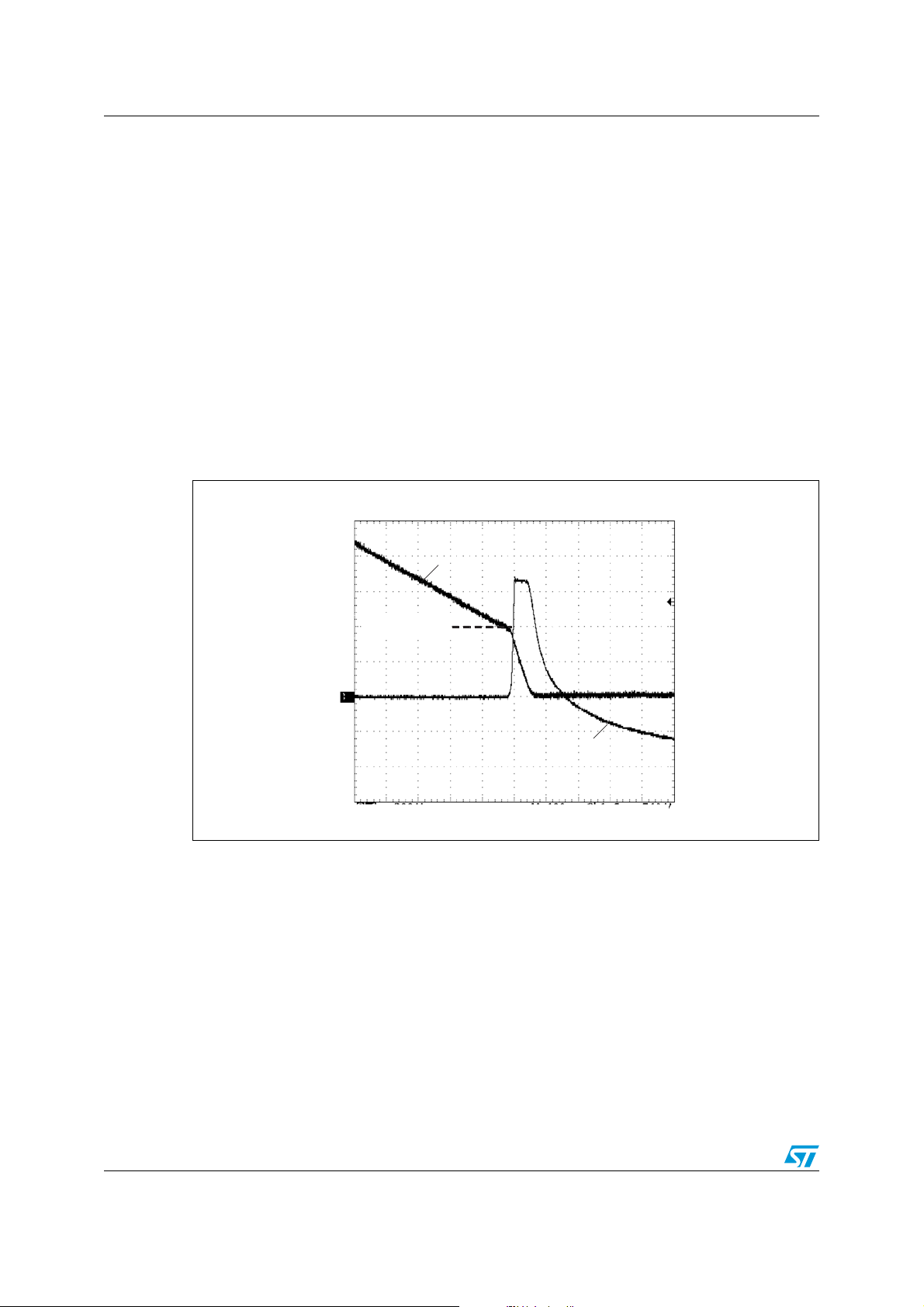
ACSs are self-protected against overvoltage. They can sustain their holding current in such
an operating mode, as shown in Figure 2.
Figure 2. Valve turn-off - typical oscillogram with the ACS108-5TA device
Ih = 20 mA
1.2 IEC 61000-4-5 standard
The IEC 61000-4-5 standard has been established to check whether systems can continue
to work after there has been a voltage surge superimposed on the mains. A standard
voltage waveform has been chosen which embodies typical overvoltages due to lightning or
the disconnection of running inductive loads from the line.
Iout (10mA/div)
Vout (200V/div)
Time: 400 µs/div
As the line to neutral surge can appear at peak mains voltage, the overall voltage can reach
2.4 kV (2 kV surge + peak mains voltage for 240 V rms line). This will be higher than the
breakdown level of the silicon devices used in appliances. To prevent the destruction of
components, designers use a varistor connected across silicon devices.
When a surge occurs and the ACS is off, the mains overvoltage is first clamped by the
device. But an excessive energy surge can raise the ACS current above its breakover level.
2/10 Doc ID 8317 Rev 5
Page 3

AN1379 ACS: an overvoltage protected AC device
Then, the switch turns on in breakover mode [2] [3]. Such an event is particularly stressful
on the semiconductor especially so if the current and its rate of increase are both high. The
worst case occurs when ACSs are driving low resistance, non inductive loads (only a few
tens of µH as a series parasitic inductance).
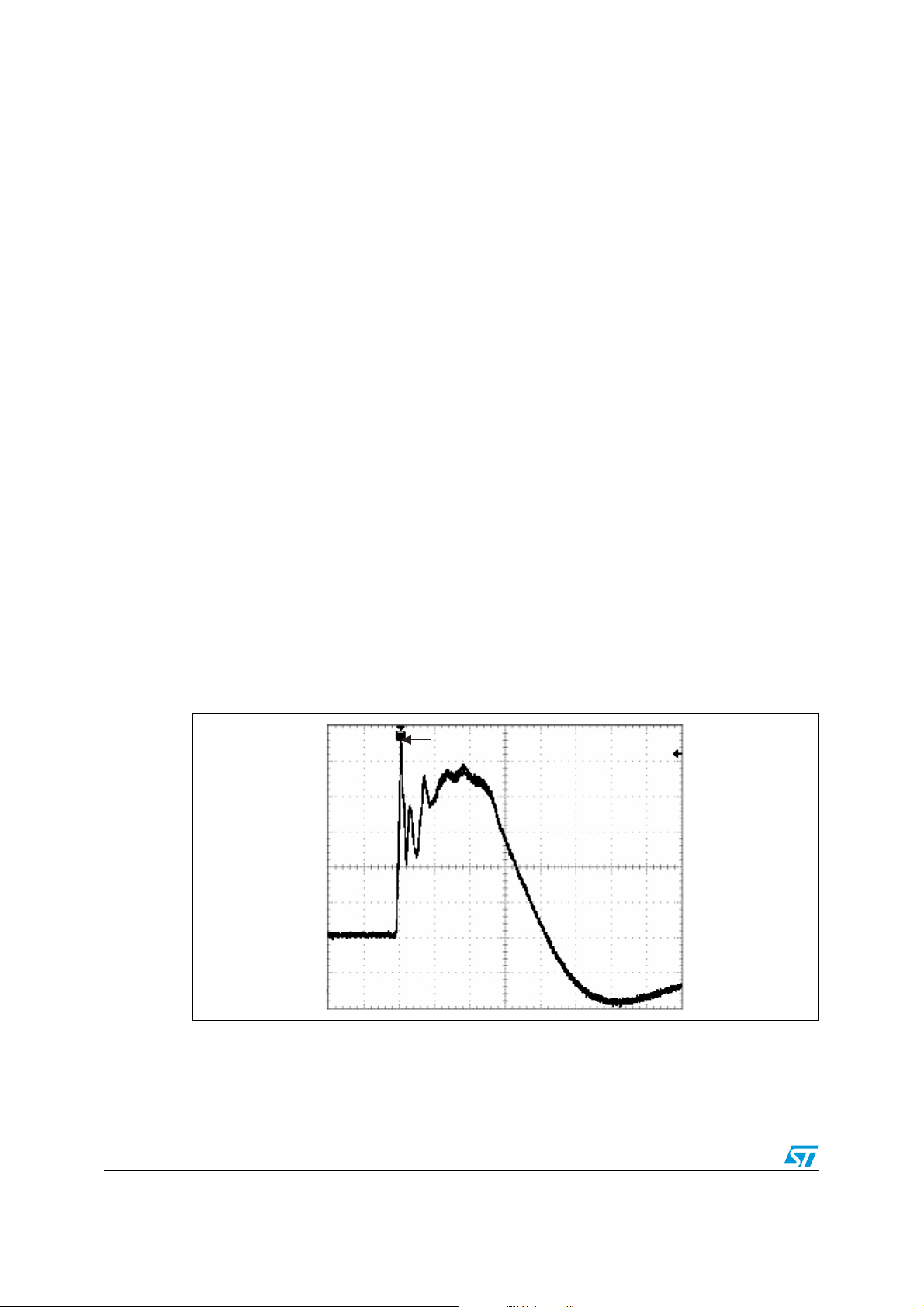
For example, Figure 3 and Figure 4 have been recorded with a thermal active door lock
system at a low temperature controlled by an ACS108-5TA device. The 2 kV surge is superimposed on the 230 V, 50 Hz mains and synchronized with its peak value, as shown in
Figure 3. Figure 4 shows the device turn on in this mode. As the load was previously off, its
resistance is cold and equals 150 ohm. In this case, the current rises at a rate of 100 A/µs
and reaches 15 A. Such transient surges would damage Triacs, but not ACSs, as they are
designed to turn on in breakover mode. The varistor is then no longer needed in parallel
across ACSs, unlike Triacs. The difference between ACS and Triac + varistor is that, with the
ACS, the load is switched on during a half or one mains cycle. This can be accepted as such
events happen a few times in the system's life.
Figure 3. 2 kV surge on the mains
VAC(500 V/div)
I
(5 A/div)
out
Figure 4. ACS breakover
VAC(200 V/div)
I
(5 A/div)
out
Doc ID 8317 Rev 5 3/10
Page 4
Fast transient immunity tests AN1379
2 Fast transient immunity tests
2.1 Standard requirements and mains filter utility
IEC 61000-4-4 tests propose two different kinds of stress. One, called the “supply test”,
consists of applying the bursts through 33 nF capacitors to the line, neutral, ground or
combinations of these terminals. The second EN61000-4-4 stressing mode is to apply the
bursts through a typical 100 pF capacitor (achieved with an aluminum sheet), directly to the
I/O ports of the system.
The I/O port test is in fact required for systems where there are control wires, as for
computers (wires between the keyboard and the central unit). But appliance manufacturers
perform similar tests to check if their products can withstand fast voltage transients.
For both cases, the system under test is placed 10 cm above the bursts generator reference
plane. As the voltage waveforms increase and decrease respectively in 5 and 50 ns, the
impedance of the parasitic capacitance between the system board and the plane is very low
for such high dynamic waveforms. This results in the application of the major part of the
burst directly across the mains supply plug of the system under test. The following figures
show the line to neutral voltage measured during a 2 kV supply test. We see that the voltage
reaches up to 1.41 kV when no filter is used at the mains input of the system. If a filter, such
as that described in Figure 7, is added, the overvoltage, caused by the 2 kV burst falls to
584 V. This is below the breakdown voltage of most Triacs used in 230 V appliances and of
ACSs. Then, there is no risk of a spurious firing due to turn on in breakover mode.
But Figure 6 also shows that, despite overvoltages being limited, high dV/dt rates are still
present. Indeed, the 500 V overvoltage is reached in less than 10 ns. Silicon devices must
therefore feature a very high dV/dt capability in order to avoid parasitic turn on. The next
paragraph summarizes some comparative analysis made on Triacs and ACSs.
Figure 5. Line to neutral voltage during 2 kV burst without mains filter
1.41 kV
4/10 Doc ID 8317 Rev 5
Page 5

AN1379 Fast transient immunity tests
Figure 6. Line to neutral voltage during 2 kV burst with mains filter
584 V584 V
2.2 ACS / Triac comparison
The tests are carried out in the following conditions:
■ Printed circuit board 10 cm above reference plane
■ A mains filter (as described in Figure 7) connected to the mains plug
■ Board embeds four Triacs (or ACSs)
■ Each Triac-A2 (or ACS-OUT) terminal linked to a 25 W light bulb (resistive loads are
chosen in order not to reduce dI/dt rates in case of firing)
■ Each gate connected to A1 or COM terminals respectively, for Triac and ACS, through a
470 ohm resistor (to be free of spurious firings coming from the microcontroller)
■ No snubber circuits added across the Triacs or ACSs
■ Ambient temperature 25 °C.
■ Burst generator programmed as required in the IEC 61000-4-4 standard (15 ms burst
duration, 3 Hz burst frequency, 5 kHz spike frequency, one second test duration).
Figure 7. Mains filter for IEC 61000-4-4 test
Rg
100 pF
100 pF
100 pF
Burst
generator
10 cm
L
0.47 µF
X2
N
2.5nF
Y2
2.5 nF
Y2
680 k
Mains filter
Reference plane
A2
2 x 1 mH
GND
Doc ID 8317 Rev 5 5/10
Page 6

Fast transient immunity tests AN1379
The high voltage output of the burst generator is connected:
– In the case of the “plug test”: to a 33 nF capacitor with its other terminal connected
to L, N, ground, or several of these terminals (as required in the IEC 61000-4-4
standard).
– In the case of the “I/O test”: to six 100 pF discrete capacitors with their other
terminal connected to the four A2 (or OUT), L and N terminals (in order to simulate
the coupling aluminum sheet).
A test is carried out for each coupling mode. The minimum burst level which causes a
spurious firing, of one of the four devices, is measured. Figure 8 gives the results of these
tests.
Sensitive Triacs and ACSs with identical gate currents were compared. For a 5 mA
maximum gate current, Z0107MA Triacs and ACS102-5TA devices were used. For a 10 mA
maximum gate current, Z0109MA Triacs and ACS108-5SA / ACS402-5SB4 devices were
used. All these components are in TO92 packages except the ACS402-5SB4 which is in
DIL20 package. One can see that using one ACS array instead of several devices is an
advantage in terms of noise immunity. Indeed, the board including four ACS108 in TO92 can
sustain up to 3.7 kV and the other, including ACS402 in DIL20, can sustain up to 4 kV.
It can be noticed that the generator used can only delivers bursts up to 4.5 kV. For some
ACS108 and ACS402 devices, this has not reached the level above which they turn on.
The different capability of these devices depends on the dV/dt characteristics. The device
can switch on due to excessive dV/dt rates. For example, Figure 9 shows, that a Z0109MA
turns on after a 17 kV/µs rate, due to a 2 kV burst coupled to the line in the “plug test”
configuration. As for the maximum junction temperature, 5 mA and 10 mA sensitivity ACSs
can sustain up to 300 V/µs and 500 V/µs respectively, whereas Triacs of similar sensitivities
only withstands 20 and 50 V/µs respectively, it is obvious that choosing ACSs will improve
the burst immunity of the electronic board.
“I/O tests” have also been carried out. The difference between Triacs and ACSs is more
difficult to prove as most of the devices sustain bursts higher than the maximum capacity of
the used generator (4.5 kV). Ta b l e 1 shows the results of these trials. In fact, the higher
immunity of ACSs could be demonstrated by removing the mains filter. In this case, the
board using ACS402-5SB4 will sustain bursts in the range of 4 kV, but for Z0109MA, the
capability drops to around 3 kV.
6/10 Doc ID 8317 Rev 5
Page 7

AN1379 Fast transient immunity tests
Figure 8. Minimum burst levels before turn on for different devices
Minimum held
burst level
above generator
capability (4.5 kV)
4 kV
3 kV
2 kV
1 kV
0 kV
TO92
DIL20
Standard
requirement
5 mA igt 10 mA igt 5 mA igt 10 mA igt
Triac ACS
Table 1. Minimum burst levels before devices turn on for I/O tests
Device Z0107MA Z0109MA ACS102-5TA ACS108-5SA
Min. level
capability
4 kV > 4.5 kV > 4.5 kV > 4.5 kV
Figure 9. Spurious firing of a Z0109MA after a 2 kV burst
dV/dt = 17kV/µs
V
A2A1
(100 V/div)
IA2(0.5 A/div)
Doc ID 8317 Rev 5 7/10
Page 8

Conclusion AN1379
3 Conclusion
The IEC 61000-4-4 standard requires that for systems working on public power networks,
the system must operate without any problem during burst voltages up to 1 kV. It has been
shown that thanks to the mains filter, which is commonly added in washing machines in
order to reduce the noise generated by universal motor brushes, Triacs and ACSs of 5 mA
sensitivity can pass the standard requirements. However, some manufacturers increase the
burst level up to 2 kV. In this case, only ACSs will fulfill the requirement without additional
components.
As for the Triacs, they will turn on due to high dV/dt rates. An RC circuit must then be added
to even out the dV/dt and designers must manage the following trade-off:
1. Reduce dV/dt rates: The snubber capacitance must be high and the snubber
resistance must be low.
2. Reduce the dI/dt rate at turn on: The snubber capacitance must be low and the snubber
resistance must be high.
Along with the fact that these snubbers and the varistors are no longer required with ACSs,
using ACS reduces design time and increases electronic board reliability.
References
1. “Thyristors and Triacs: holding current - an important parameter”, Application note
AN302, Revision 3, STMicroelectronics, March 2008.
2. L.Gonthier, “A New Solid State Switch for Home Appliances”, International Appliance
Technical Conference, West Lafayette, Indiana (USA), May 1999.
3. L.Gonthier, “A New Overvoltage-Protected Logic Level AC Switch Thanks to Functional
Integration”, European Conference on Power Electronics and Application (EPE'99),
Lausanne (Switzerland), September 1999.
8/10 Doc ID 8317 Rev 5
Page 9

AN1379 Revision history
4 Revision history
Table 2. Document revision history
Date Revision Changes
June-2001 3 Previous issue.
24-Apr-2009 4
Reformatted to current standards. Full technical review for current
products.
22-Jun-2010 5 Added trademark information in Figure 1.
Doc ID 8317 Rev 5 9/10
Page 10

AN1379
Please Read Carefully:
Information in this document is provided solely in connection with ST products. STMicroelectronics NV and its subsidiaries (“ST”) reserve the
right to make changes, corrections, modifications or improvements, to this document, and the products and services described herein at any
time, without notice.
All ST products are sold pursuant to ST’s terms and conditions of sale.
Purchasers are solely responsible for the choice, selection and use of the ST products and services described herein, and ST assumes no
liability whatsoever relating to the choice, selection or use of the ST products and services described herein.
No license, express or implied, by estoppel or otherwise, to any intellectual property rights is granted under this document. If any part of this
document refers to any third party products or services it shall not be deemed a license grant by ST for the use of such third party products
or services, or any intellectual property contained therein or considered as a warranty covering the use in any manner whatsoever of such
third party products or services or any intellectual property contained therein.
UNLESS OTHERWISE SET FORTH IN ST’S TERMS AND CONDITIONS OF SALE ST DISCLAIMS ANY EXPRESS OR IMPLIED
WARRANTY WITH RESPECT TO THE USE AND/OR SALE OF ST PRODUCTS INCLUDING WITHOUT LIMITATION IMPLIED
WARRANTIES OF MERCHANTABILITY, FITNESS FOR A PARTICULAR PURPOSE (AND THEIR EQUIVALENTS UNDER THE LAWS
OF ANY JURISDICTION), OR INFRINGEMENT OF ANY PATENT, COPYRIGHT OR OTHER INTELLECTUAL PROPERTY RIGHT.
UNLESS EXPRESSLY APPROVED IN WRITING BY AN AUTHORIZED ST REPRESENTATIVE, ST PRODUCTS ARE NOT
RECOMMENDED, AUTHORIZED OR WARRANTED FOR USE IN MILITARY, AIR CRAFT, SPACE, LIFE SAVING, OR LIFE SUSTAINING
APPLICATIONS, NOR IN PRODUCTS OR SYSTEMS WHERE FAILURE OR MALFUNCTION MAY RESULT IN PERSONAL INJURY,
DEATH, OR SEVERE PROPERTY OR ENVIRONMENTAL DAMAGE. ST PRODUCTS WHICH ARE NOT SPECIFIED AS "AUTOMOTIVE
GRADE" MAY ONLY BE USED IN AUTOMOTIVE APPLICATIONS AT USER’S OWN RISK.
Resale of ST products with provisions different from the statements and/or technical features set forth in this document shall immediately void
any warranty granted by ST for the ST product or service described herein and shall not create or extend in any manner whatsoever, any
liability of ST.
ST and the ST logo are trademarks or registered trademarks of ST in various countries.
Information in this document supersedes and replaces all information previously supplied.
The ST logo is a registered trademark of STMicroelectronics. All other names are the property of their respective owners.
© 2010 STMicroelectronics - All rights reserved
Australia - Belgium - Brazil - Canada - China - Czech Republic - Finland - France - Germany - Hong Kong - India - Israel - Italy - Japan -
STMicroelectronics group of companies
Malaysia - Malta - Morocco - Philippines - Singapore - Spain - Sweden - Switzerland - United Kingdom - United States of America
www.st.com
10/10 Doc ID 8317 Rev 5
 Loading...