

Page 1

AN1365
APPLICATION NOTE
GUIDELINES FOR MIGRATING ST72C254
APPLICATIONS TO ST72F264
INTRODUCTION
This application note provides information on us ing ST72264 new series in an application ori ginally designed for the ST72254, 215, 216, 104 series.
1 FEATURE OVE RVI EW
Feature
Package SDIP32/SO28 (no change)
Program Memory FLASH/ROM
Operating Supply 3.2V to 5.5V 2.7V to 5.5V
Register Map 128 bytes (no change)
I/Os 28 pins (see Section 2.2 Pinout)
Slow Mode Yes
Active-HALT No Yes (4096 t
Nested Interrupts No Yes (not by default)
Watchdog Yes
16-bit Timer 1212
SPI Yes
SCI No Yes
2
I
C No Yes No Y es
ADC No Yes (8-bit) No Yes (10-bit)
LVD 3 Levels (CFlash and XFlash levels may differ, refer to the datasheet)
CSS Yes (fixed frequency) -> CRSR No
Emulator ST7MDT1-EMU2B and ST7MTD1-DVP2 ST7MDT10-EMU3
Programming
2)
tools
1)
ST72104 ST72215 ST72216 ST72C254 ST72260 ST7226 2 ST72F264
delay on wake-up)
CPU
2 (minor change in
PWM and One Pulse modes)
ST7MDT1-EPB2 and ST7 MT D 1 - DVP2
ST7MDT10 -EPB and ST7MDT10-
DVP3
Note 1: refer to the corresponding datasheets for more information on electrical characteristics.
Note 2
AN1365/0504 1/13
:
Go to
http://www.st.com > Products > Product Support > Microcontrollers - Forum
informati on on third-party tools.
for
Rev. 2.0
1
Page 2

GUIDELINES FOR MIGRATING ST72C254 APPLICATIONS TO ST72F264
2 PINOUT CO MPATIBILITY
2.1 PACKAGE
All devices are available in SDIP32 and SO28 packages.
2.2 PINOUT
Some pins have been changed in the pinout of the ST 72F264 (and s ubsets) device to add the
SCI peripheral (see Table 1) and to move the ISP pins (which have be come ICC pi ns) (see
Table 2).
For more information about ICC (In-Circuit Communication) protocol, please refer to the ST7
FLASH Programming and ICC Reference Manuals av ailable on Internet (http://www.st.com).
Table 1 . Addition of SCI Pins
ST72F264 only
SDIP32 Package TDO (pin 20) RDI (pin 22)
SO28 Package TDO (pin 18) RDI (pin 20)
Table 2. Pin Changes
ST72C254 and Subsets ST72F264 and Subsets
SDIP32 Package SO28 Package SDIP32 Package SO28 Package
ISPCLK (pin 5) ISPCLK (pin 5) ICCCLK (pin 29) ICCCLK (pin 25)
ISPDATA (pin 6) ISPDATA (pin 6) ICCDATA (pin 28) ICCDATA (pin 24)
TDO is the Transmit Data Output pin and RDI is the Receive Data Input pin of the SCI (Serial
Communication Interface) peripheral.
2/13
2
Page 3
GUIDELINES FOR MIGRATING ST72C254 A PPLICATIONS TO ST72F264
3 TIMING
3.1 CYCLE ACCURACY
All timings are compatible between the ST72C254 and the ST72F264 devices except internal
timings linked to the cycle accuracy. The ST72C254 is based on latches (gates) while the
ST72F264 is bas ed o n R TL (fl ip-flop). T her efore , a d ifferen ce of a h alf c ycle may oc cur between those two devices.
This means that all software with timings based on fixed processor cycle times (a practice not
recommended) must be verified in detail. An example of this would be a software wait loop implemented as a sequence of NOP instructions as opposed to polling a busy bit.
This internal difference does not affect the general timings.
3.2 CLOCK SECURITY SYSTEM (CSS)
The backup oscillator of CSS available in the ST72C254 device (and subsets) has a fixed frequency between 250 kHz and 550 kHz in normal conditions (T=25° and Vdd=5V).
In the ST72F264 device (and subsets), there is no backup oscillator frequency.
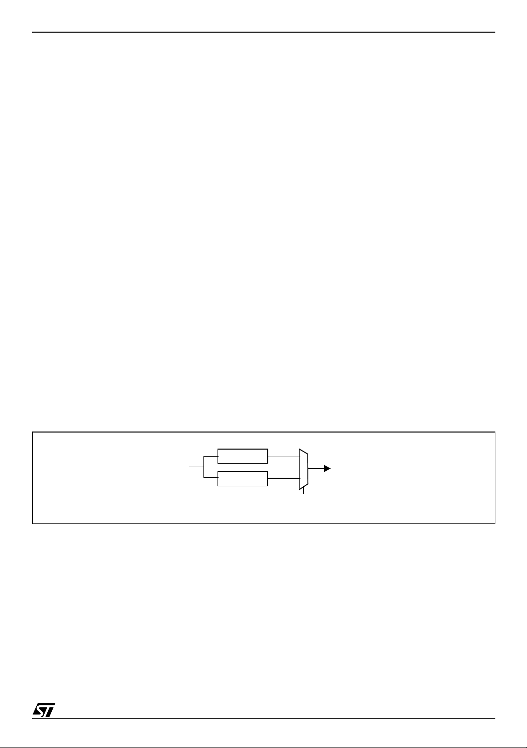
3.3 PHASE LOCKED LOOP (PLL)
A PLL has been added in the ST72F264 in order to be abl e to multiply the oscillator frequency
by 2 (for a f
input frequency between 2 and 4 MHz). This PLL is activated through an op-
OSC
tion bit.
Figure 1. PLL Dia gram
f
OSC
PLL x 2
/ 2
0
1
PLL OPTION BIT
f
OSC2
Note: Use of the PLL with the internal RC oscillator is not supported.
3/13
Page 4
GUIDELINES FOR MIGRATING ST72C254 APPLICATIONS TO ST72F264
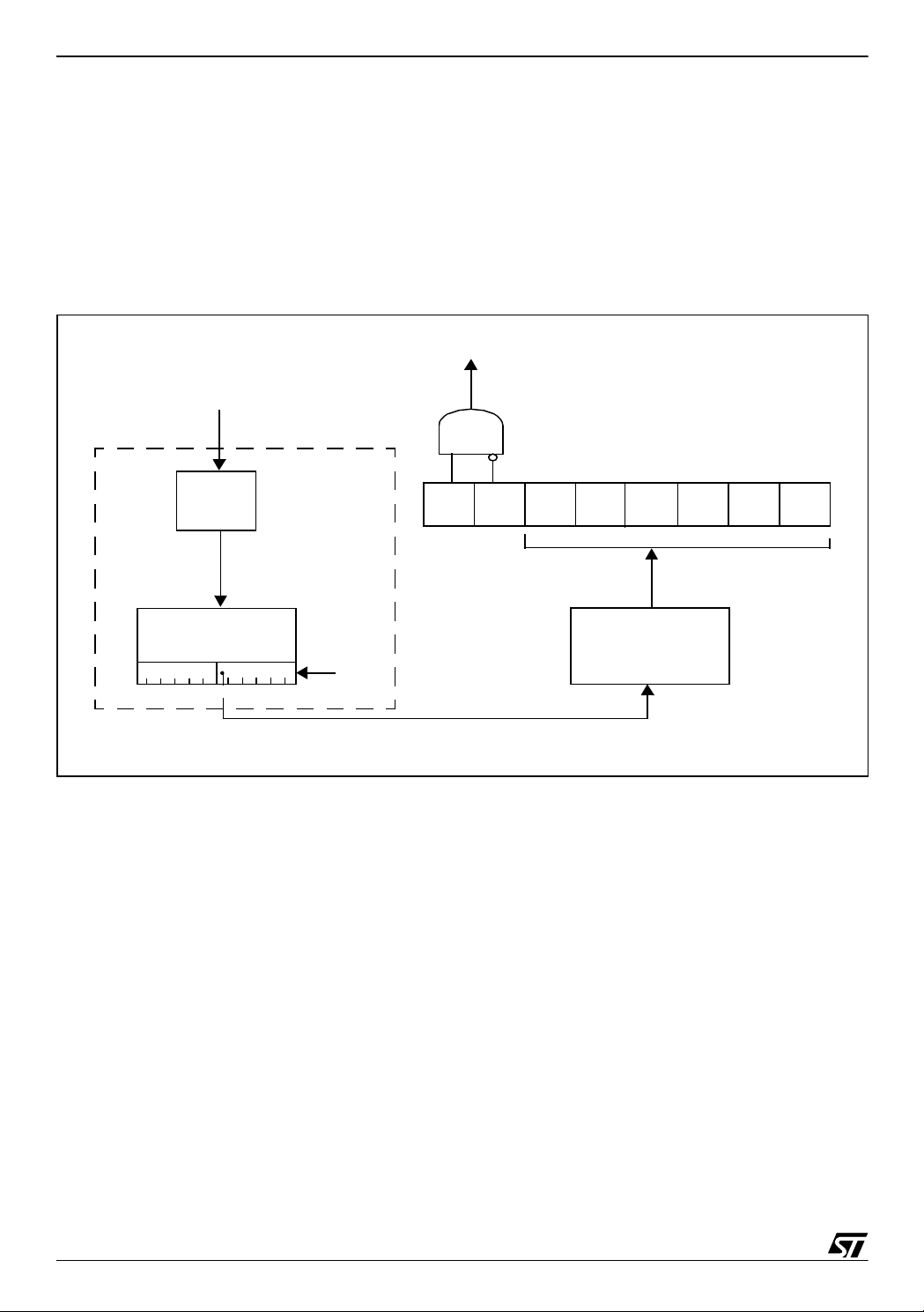
3.4 WATCHDOG TIMINGS
In the ST72F264, the watchdog timeout does not have an exact duration as in the ST72C254.
It may vary between the min. and max. times specified in Figure 3.. To guarantee upward
compatibility, you have to take this into account when you develop your software. The reason
for this change is that the watchdog counter has been grouped with the Active-HALT counter
and SLOW mode prescaler to enhance power consumption and EMC performance.
Figure 2. Watchdog Bloc k Diagram
f
OSC2
RESET
MCC/RTC
WATCHDOG CONTROL REGISTER (WDGCR)
DIV 64
12-BIT MCC
RTC COUNTER
MSB LSB
11
56
TB[1:0] bits
(MCCSR
0
Register)
WDGA
The watchdog counter is no longer clocked by f
divided by 16 384 (f
if the PLL is disabled).
f
CPU
is the PLL out put freq uency whe n the PLL is activ ated or f
OSC2
CPU
T5
T6 T0
T4
T3
6-BIT DOWNCOUNTER (CNT)
WDG PRESCALER
DIV 4
T2
T1
(as it was for the ST72C254) but by f
OSC
OSC2
/2 =
In the ST72F264 datasheet, the linear relationship between the 6-bit value to be loaded in the
Watchdog Counter (CNT) and the resulting timeout duration in milliseconds is described. This
can be used for a quick calculation without taking the timing variations into account.
If more precision is needed, use the formulae in Figure 3..
4/13
Page 5

GUIDELINES FOR MIGRATING ST72C254 A PPLICATIONS TO ST72F264
WHERE:
Figure 3.
t
t
t
CNT = Value of T[5:0] bits in the WDGCR register (6 bits)
MSB and LSB are values f rom th e table b elow de pending on the timebase selecte d by t he T B[1:0] bits
in the MCCSR register
To calculate the m i ni m um W at chdog Timeout (t
IF THEN
To calculate the maximum Watchdog Timeout (t
Exact Timeout Duration (t
= (LSB + 128) x 64 x t
min0
= 16384 x t
max0
= 125ns if f
OSC2
TB1 Bit
(MCCSR Reg.)
0 0 2ms 4 59
0 1 4ms 8 53
1 0 10ms 20 35
1 1 25ms 49 54
CNT
<
(MCCSR Reg.)
MSB
------------4
OSC2
OSC2
TB0 Bit
ELSE
OSC2
=8 MHz
t
mintmin0
t
mintmin0
Selected MCCSR
=
and t
min
Timebase
+=
16384 CNT
16384 CNT t
)
(f
max
MSB LSB
min
× 192 L SB+()64
max
OSC2
):
××+
4CNT
---------------- -
–
):
= 8 MHz)
osc2
MSB
+
××
4CNT
---------------- MSB
×
t
osc2
IF THEN
CNT
MSB
-------------
≤
4
ELSE
t
=
maxtmax0
t
maxtmax0
16384 CNT t
+=
16384 CNT
× 192 L SB+()64
××+
–
osc2
4CNT
---------------- MSB
4CNT
+
××
---------------- MSB
×
t
osc2
Note: In the above formulae, division results must be rounded down to the next integer value.
Example:
With 2ms timeout selected in MCCSR register
Value of T[5:0] Bits in
WDGCR Register (Hex.)
00 1.496 2.048
3F 128 128.552
Min. Watchdog
Timeout (ms)
t
min
Max. Watchdog
Timeout (ms)
t
max
Note: The timing variation shown in Figure 3. is due to the unknown status of the prescale r when writing
to the CR register.
5/13
Page 6

GUIDELINES FOR MIGRATING ST72C254 APPLICATIONS TO ST72F264
4 REGISTER MAP
In the ST72F264, some register addresses and bit locations are changed. These changes
have made it possible to use the free locations to add new features.
Note: For easy softw are migration, two general rules have to be followed:
■
All “reserved” byte memory areas must never be “read” or “write”.
■
All “reserved” or “unused” bits must be left unchanged when accessing the byte.
4.1 REGISTER ADDRESS
These changes are classified in three groups:
1. N ew features added: Interrupt Controller (ITC), Main Clock Controller (MCC), Ser ial Communications Interface (SCI), Flash Control/Status Register (FCSR).
2. CRSR (Clock, Reset, Supply Control/Status Register) has been replaced by the SICSR
(System Integrity Control/Status Register). Two bits relative to the AVD (Auxilia ry Voltage
Detector) feature have been added into the SICSR register. Bits relative to the CSS ar e no
longer used.
SPISR (Serial Peripheral Interface Status Register) changed to SPICSR (Serial Peripheral
Interface Control Status Register). Refer to the Section 5.3.1 for more information.
3. ADC registers changed.
Please, refer to the datasheet for the description of the new features.
Note: These register address changes can be easily performed if you group all the register
definitions in a single header file.
6/13
Page 7

GUIDELINES FOR MIGRATING ST72C254 A PPLICATIONS TO ST72F264
Figure 4. Register Map Modifications
ST72C254 ST72F264
@Block
Register
Label
0020h MISCR1
0021h
0022h
0023h
SPI
SPIDR
SPICR
SPISR
0024h WDG WDGCR
0025h CRSR
0040h MISCR2
0070h
0071h
ADC
ADCDR
ADCCSR
@Block
001Ch
001Dh
1
001Eh
001Fh
ITC
Register
Label
ISPR0
ISPR1
ISPR2
ISPR3
0020h MISCR1
0021h
2
2
0022h
0023h
0024h WDG WDGCR
SPI
SPIDR
SPICR
SPICSR
0025h SICSR
1
0026h MCC MCCSR
0050h
0051h
0052h
1
0053h
SCI
0054h
3
0055h
0056h
SCISR
SCIDR
SCIBRR
SCICR1
SCICR2
SCIERPR
SCIETPR
006Fh
0070h
ADC
0071h
1
0072h FCSR
ADCCSR
ADCDRH
ADCDRL
7/13
Page 8

GUIDELINES FOR MIGRATING ST72C254 APPLICATIONS TO ST72F264
4.2 REGISTER MODIFICATIONS
4.2.1 CRSR Register
The CRSR (Clock, Reset and Supply Register) register has been replaced by the SICSR
(System Integrity Control/Status Reg ister) register (se e Fig ure 5.). This SIC S R register contains the bits related to the AVD feature.
Figure 5. CRSR Register Changes
CRSR (0025h)
Clock Reset and Supply Register
4.2.2 SPI/SS
The SP I SS
70
000
LVD
RF
CSSIE
CSSDWDG
RF
0
pin
pin alternate function is controlled from the MISCR2 like previously, but these
SICSR (0025h)
System Integrity Control/Status Register
70
AVDIEAVDFLVD
0
000
RF
WDG
RF
control bits have also been duplicated into the SPICSR register in three unused locations.
Figure 6. SS
70
0000MODSODSSMSSI
pin control
MISCR2 (0040h)
70
SPIF
WCO
L
OR
MOD
0 SOD SSM SSI
F
SPICSR (0023h)
SPI Control/Status Register
Both registers can be used to control the SS
8/13
pin.
Page 9

GUIDELINES FOR MIGRATING ST72C254 A PPLICATIONS TO ST72F264
5 NEW FEATU RES AN D PERIPHERALS
5.1 NESTED INTERRUPTS
A nested interrupt feature has been added to the ST72F264. By default, the interrupt management is concur rent. S ome dedi cated regi sters (ISP Rx) m ake it possib le for the use r to configure the priority level (up to 4) for all the interrupts. Please refer to the datasheet for more information.
5.2 16-BIT TIMER PWM AND ONE PULSE MODE
The 16-bit tim er of the ST72C2 54 h as been mod ified in the ST72 F264 t o im prove th e P WM
and One Pulse modes. If you use either of these two modes, you may need to cha nge your
software when transferring code from the ST72C254 to the ST72F264. All the other modes of
the timer do not change.
5.2.1 PWM Mode
To avoid any uncontrolled status on the PWM output, a double buffering on the output compare registers (2 x 16 bits) is implemented in the ST72F264. This double buffering is not
present in the ST72C254.
In the ST72F264 PWM mode, an y new values written in the fo ur OC1R and OC 2R registers
are taken into account only at the end of the PWM period (OC2 event) to avoid spikes on the
PWM output.
Note: Any modification on the OC1R and OC2R registers m u st be done just after the OC 2
event (using the ICF1 interrupt routine for example).
5.2.2 One Pulse Mode
When the ICAP1 event occurs (on falling or rising edge), the following sequence occurs:
1. IC1R is loaded with the value of the counter when the event occurred (not FFFDh as in the
ST72C254)
2. The counter is immediately reset to FFFCh (not at the end like in the ST72C254)
3. OLVL2 is applied to OCMP1 pin if OC1E=1
4. ICF1 is set
9/13
Page 10

GUIDELINES FOR MIGRATING ST72C254 APPLICATIONS TO ST72F264
5.3 SPI
5.3.1 Control/Status register bits
The SPISR in the ST72C254 has been replaced by the SPICSR in the ST72F264 (refer to
Figure 4.). Their differences are the following ones:
■
the SPI SS pin alternate function is controlled from the MISCR2 as previously, but these
control bits have also been duplicated into the SPICSR register.
■
the Overrun flag has been added into the ST72F264 (SPICSR register).
5.3.2 HALT mode
The ST72F264 is able to exit from HALT mode through an SPI interrupt. This is not the case
in the ST72C254. To guarantee upward compatibility, if the SPI is used in slave mode, the SPI
interrupt must be masked (via the SPE or SPIE bits) during HALT mode to avoid any unwanted wake-up events.
5.4 10-BIT ADC
To meet applicati on r equ iremen ts fo r in creased res oluti on, the ST 72 F264 has a 10-b it ADC
compared to the 8-bit ADC in the ST72C254. For upward compatibility, both ADCs have identical control registers and operating modes. The 8 m o st significant bits of the ST72F264 data
register (ADCDRH) are used in place of the ADCDR register of the ST72C254. The 8 least
significant bits of the ST72F264 d ata register (ADCDRL) have been adde d to reach a 1 0-bit
conver si on . I f ADCDR L is re ad first, ADCDRH is l ock e d unt i l rea d (wh i ch mea ns t h at no max imum time is i mposed betw een an ADCD RL r ead and an ADCDRH read) and a 10-bit conversion will be performed. Then, ADCDRL and ADCDRH are ensured to correspond to the same
conversion.
If ADCDRH is read first, ADCDRL is lost and an 8-bit conversion equivalent to the ST72C254
one will be performed.
5.5 MISCELLANEOUS
Many new features have been added in the ST72F264 (refer to Figure 4.):
■
MCC (Main Clock Controller)
■
ITC (Interrupt Controller)
■
FSCR register (Flash Status Control Register)
■
SCI (Serial Communication Interface) peripheral
Please, refer to the datasheet for more information concerning the operation of all these features and peripherals.
10/13
Page 11

GUIDELINES FOR MIGRATING ST72C254 A PPLICATIONS TO ST72F264
6 OPTION BYTES
Option bits have been added, split or replaced in the ST72F264 c ompared to the S T72C254
(see Figure 7 .):
■
Oscillator type bits have been added in order to select a best range of backup safe oscillator
■
CFC (Clock Filter Control) bit has been removed
■
FMP (Full Memory Protection) bit has been split into 2 bits: FMP_R (read protection) and
FMP_W (write protection)
■
SEC[1:0] bits have been added to select the ST72F264 sector 0 size
■
PLL selection bit has been added
■
External RC clock option is no longer supported with ST72F264 device.
For more information concerning these option bits, please refer to the datasheet.
Figure 7. ST72C254 and ST72F264 Optio n Byt e s
ST72C254 Option Bytes
USER OPTION BYTE 0
70
Reserved
EXTIT FMP CFC OSC2 OSC1 OSC0 LVD1 LVD0
70
USER OPTION BYTE 1
ST72F264 Option Bytes
USER OPTION BYTE 1
15 8
OSC
OSC
OSC
OSC
OSC
EXTIT 1
■
LVD low and high configuration levels have been swapped:
TYPE
1
TYPE
0
RNGE
2
RNGE
1
RNGE
PLL
OFF
0
70
WDG
HALT
USER OPTION BYTE 0
WDG
VD1 VD0 SEC1 SEC0 FMPR FMPW
SW
WDG
HALT
WDG
SW
11/13
Page 12

GUIDELINES FOR MIGRATING ST72C254 APPLICATIONS TO ST72F264
Figure 8. ST72C254 and ST72F264 LVD Configuration Levels
ST72C254
Configuration LVD1 LVD0
LVD Off 11
Highest threshold 10
Medium threshold 01
Lowest threshold 00
ST72F264
LVD1 LVD0 Configuration
11 LVD Off
00Highest threshold
01Medium threshold
10Lowest threshold
Moreover, please take note that LVD levels values between the ST72C254 and the ST72F264
may differ a little bit. Please, refer to the datasheet of the respective devices (Electrical parameters part) to get them.
12/13
Page 13

GUIDELINES FOR MIGRATING ST72C254 A PPLICATIONS TO ST72F264
“THE PRESENT NOTE WHICH IS FOR GUIDANCE ONLY AIMS AT PROVIDING CUSTOMERS WITH INFORMATION
REGARDING THE IR PRO DUCT S IN OR DER FO R THEM TO SAV E TIME . AS A RES ULT, STMIC ROEL ECTR ONI CS
SHALL NOT BE HELD LIABLE FOR ANY DIRECT, INDIRECT OR CONSEQUENTIAL DAMAGES WITH RESPECT TO
ANY CLAIMS ARISING FROM THE CONTENT OF SUCH A NOTE AND/OR THE USE MADE BY CUSTOMERS OF
THE INFORMATION CONTAINED HEREIN IN CONNECTION WITH THEIR PRODUCTS.”
Information furnished is believed to be accurate and reliable. However, STMicroelectronics assumes no responsibility for the consequences
of use of such information nor for any infringement of patents or other rights of third parties which may result from its use. No license is granted
by implic ation or oth erwise unde r any patent or patent r i ghts of STMi croelectroni cs. Speci fications me ntioned in this publicat i on are subject
to change without notice. This publication supersedes and replaces all information previously supplied. STMicroelectronics products are not
authorized for use as critical components in life su pport device s or systems without express written approval of STMicroelectronics.
The ST logo is a register ed t rademark of ST M i croelectroni c s.
All other nam es are the pro perty of their respective ow ners
© 2004 STMi croelectroni cs - All rights reserved
STMicroelectron i cs GROUP OF COMPANIES
Australia – Belgium - B razil - Canad a - China – Czech Republic - Finl and - France - Ger many - Hong Kong - India - Israel - Italy - Japan -
Malaysia - Malta - Morocco - Singapore - Spain - Sweden - Switzerland - United Kingdom - United States
www.st.com
13/13
 Loading...