

Page 1

AN1353
Application note
ASD
ST62000C software description for cooling thermostat applicatons
1 Introduction
In this document, we explain the software of an Electronic thermostat bread board. The
demonstration kit has been developped by STMicroelectronics and is available under
THERM01EVAL reference.
This board illustrates the operation of a low cost electronic thermostat for 220-240V 50Hz
cold appliances, including STMicroelectronics ACS102-5TA, ACST6-7ST and ST62 devices.
The microcontroller will ensure four functions:
● Temperature regulation (temperature capture through NTC resistor + Hysteresis
regulation).
● Compressor monitoring: the motor is controlled depending on fridge temperature. To
start it, the starting triac Ts and the run triac Tr are triggered simultaneously for 500ms.
Then, only the run triac will continue to conduct.
● Overcurrent detection: this is based on the measure of the peak current using a shunt
resistor. During the one second (500 ms+500 ms) of starting transient, this routine
does not run.
● Internal light bulb control.
2 Hardware configuration
2.1 General information
The power supply of the microcontroller is a capacitive one. Its particularity is that the VSS
is 5V less than the Neutral. This power supply can be called a “negative supply”. This
generates flowing out current from the ACS/ACST gates (ACS are triggered only with a
negative gate current). This feature must also be kept in mind when the overcurrent
detection is implemented. It will define in which polarity the current can be sensed.
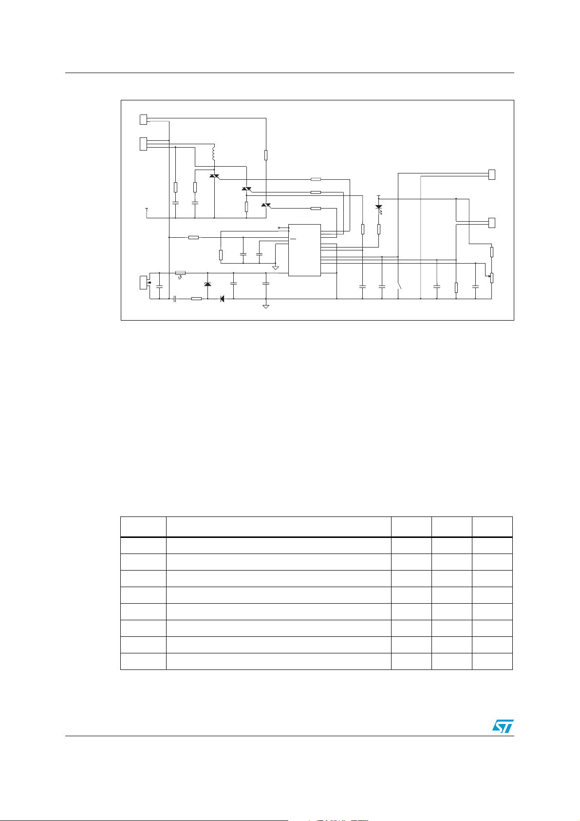
Figure 1 illustrates the board electrical circuit.
January 2006 Rev 2 1/17
www.st.com
Page 2
Hardware configuration AN1353
Figure 1. Bread-board schematic
J1
1
BULB
2
J4
L
Run
N
L
C4
10 nF X2
Start
R13
51R
C5
1nF
FUSE 6 A / 250 V
F1
C1
470nF X2
R6
470K
R11
47R 1/2 W
L_PCB
6µH
Tr
Start ACST6
R14
51R
C6
1nF
R10
50m 1/2 W
R9
47K
VDD
+
D2
6V2 1.3W
D3
C11
680pF
C3
2200µF / 10 V
Ts
Run ACST6
C2
100nF
R1
33R 1/2W
C12
1 µF
Tb
Bulb ACS102
2
3
4
6
5
1
U1
OSCIN
OSCOUT
NMI
RST
VPP/TEST
VDD
ST62T00C
PB0/AIN
PB1/AIN
PB3/AIN
PB6/AIN
PB7/AIN
PB5/AIN
J3
R2
160R
R3
160R
R4
360R
15
PA1
14
PA2
13
PA3
12
11
10
8
7
9
16
VSS
VDD
D1
LED
R5
R7
33k
1.5K
C10
2.2nF
doorswitch
2.2nF
S2
C9
R8
C8
62K
2.2nF
1
DOOR
2
J2
1
NTC
2
R12
1K
POT A
100K
C7
2.2nF
MOTOR
MAINS
1
2
3
VDD
J5
1
2
3
Note the following features on the MCU hardware environment:
● The clock is achieved by the internal oscillator
● No external reset circuit is used, thanks to the Low Voltage Detector option of the MCU
● The Zero Voltage Crossing (ZVC) event is sensed through R6 by the NMI pin.
2.2 I/O port configuration
The following table explains what the I/O ports are used for, and how they are configured,
beginning with the Port B which is configured in Input (except for PB1 which is configured as
a push pull output).
All the inputs are configured with a pull up resistor, except for when they are used as an
ADC input. No In-terrupt is active on any of these pins.
Table 1. Port B configuration registers
Pin Name USE DDR OR DR
PB0 Not used 0 0 0
PB1 Switch ON the LED / Switch OFF the LED 1 1 0/1
PB2 Not existing for ST6200 0 0 0
PB3 SHUNT voltage Analog Input / Input with pull up 0 1/0 1/0
PB4 Not existing for ST6200 0 0 0
PB5 Temperature order Analog Input / Input with pull up 0 1/0 1/0
PB6 Door switch information 0 0 0
PB7 Cabinet temperature Analog Input / Input with pull up 0/0 1/0 1/0
All port A pins are configured as push pull outputs. Table 2 details the option choices and
configuration reg-isters.
2/17 Rev 2
Page 3

AN1353 Main program
Table 2. Port A configuration registers
Pin Name USE DDR OR DR
PA1 START ACST6 ON / START ACST6 OFF 1 1 0/1
PA2 RUN ACST6 ON / RUN ACST6 OFF 1 1 0/1
PA3 LIGHT BULB ON / LIGHT BULB OFF 1 1 0/1
3 Main program
3.1 Mains period measurement
As the board does not embed an oscillator or resonator, the internal resonator of the MCU is
used to achieve the clock. But, in this case, the running frequency is given within a range of
20%. This is not enough to ensure an optimum pulse gate current control with a power
consumption as little as possible.
To increase the timer accuracy, the MCU uses the Zero Voltage Crossing (ZVC) events to
have time infor-mation. The LINE voltage is connected to the NMI pin through a high
impedance resistor. An interruption will then occur at each ZVC event. The MCU has just to
launch the timer decrementation between two NMI interrupts to calculate how much one
must load the TCR register to count down 20 ms.
Of course, in normal operation, the timer can be used for other tasks than counting the
mains period. The period measurement will then be based on the rest of time from the last
timer utilization and the next NMI interrupt. This measured time is saved as DELTAT (see
Figure 2) by the software. The 20 ms will then equal the DELTAT, plus the sum of times T1 to
T3, plus the time lost due to calculator operations between each timer stop and launch (see
Section 4.3).
Note: Such a method is only valid when the mains frequency is know in advance; i.e. for a board
dedicated to one range of AC mains voltage. In our case, the software and hardware are
dedicated to 220/240 V 50 Hz applications.
Rev 2 3/17
Page 4
Main program AN1353
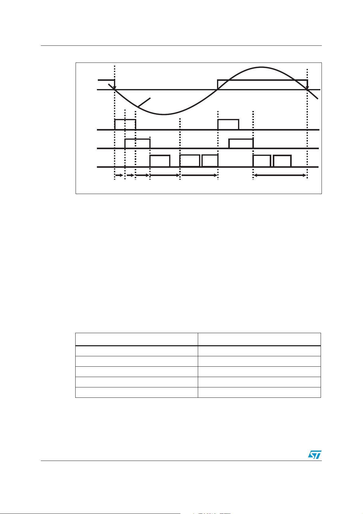
Figure 2. Timing definition
NMI
Mains Voltage
PA3
PA1 / PA2
Subroutines
Calcul
Delay 1
Current
Measure
Motor
Status
T1 T2 T3 T4 T5
3.2 Subroutines execution time checking
In order not to miss the timer interrupt events, the CPU must be completely free and ready
to check the timer interrupt flag. This means that all subroutines must be completed before
the expected end of the timer decrementation.
Figure 2 shows that the subroutines are placed at different moments, depending on their
length. For exam-ple, the longest CPU action is when the MCU calculates the T1 to T5
delays. This action can last up to more than 7.2 ms for a 4 MHz MCU clock frequency. Then,
there is not enough time available between two timer interrupts to calculate these five
values. This is the reason why the delay calculation subroutine has been split into two parts
(Calcul-Delay_1 and Calcul-Delay_2). These two parts are respectively placed during T4
and DELTAT decounts
Ta bl e 3 gives the maximum duration of each subroutine (for a 4 MHz clock frequency, and
the for the lon-gest software loops).
Table 3. Subroutines maximum durations
Calcul
Delay 2
Loads
Control
DELTAT
SUBROUTINE NAME MAXIMUM TIME
Loads_Control 0.93 ms
Motor_Status 0.26 ms
Current_Measure 0.92 ms
Calcul_Delay_1 1.75 ms
Calcul_Delay_2 5.49 ms
Ta bl e 4 gives the code execution maximum times for all the instructions written in the
software, before each subroutine (“code execution time” column). Then, according to the
implemented durations, the time, still available for the CPU, is given with a 0.2 ms safety
margin.
4/17 Rev 2
Page 5

AN1353 Main program
Table 4. CPU available time
Name
T1 0.45 0.25 0 0
T2 1.05 0.13 0 0.72
T3 1.75 0.13 0 1.42
T4 3.95 0.85 (T50 Hz average) 1.75 1.15
T5 2.80 0.09 0.26 + 0.92 1.33
DELTAT 6.75 0.08 5.49 + 0.93 0
TOTAL 4.62
Duration
(ms)
Code execution time
(ms)
3.3 Start-up and smart reset
At each RESET interrupt, the program first checks if the data stored in the RAM are as
scheduled or not. In-deed, a RESET can occur without the supply voltage having fallen
below VRM (Data retention parameter: 0.7 V). In this case, a whole start-up is not
necessary, and the program can keep working with the previous RAM data. This is helpful in
order to avoid missing loads control when a RESET occurs, due to an EMI problem for
example.
If the checked RAM registers are not as expected, then a complete initialization procedure is
launched (see Appendix B). This routine, among other things, configures the A and B ports,
waits 100 ms before go on (wait-ing for the stabilization of the supply), and measures the
mains period for the first time.
Subroutines time sum
(ms)
Available time (ms)
If the RAM area is adequate, then a “Smart Reset” can be performed. Only the registers
which are used to store internal sub-routines variables are cleared. Only the main registers
keep their previous values (motor status, etc.).
It is important to note that this start-up procedure can miss firing some loads during one
mains cycle. This is why, if the motor was at start-up state before a “Smart Reset”, it is better
to stop the motor. This avoids switching both the Tr and Ts devices ON together when the
split phase capacitor can be charged (refer to AN1354). This is done by simply setting to
high level the overcurrent detection flag.
Rev 2 5/17
Page 6

Gate current pulses AN1353
4 Gate current pulses
4.1 General description
The gate current pulses are generated during the main program (refer to Appendix A and
also to Figure 2). The Port A pins are set or reset depending on the information defined by
the sub-routines described in para-graph 5.
Annex 1 gives the flowchart of the main program. The ZVC events are sensed thanks to bit
0 of the FLAG register, which is only set during the NMI interrupt. The end of timer
decrementations are also sensed by bit 1 of the FLAG register, which is set during timer
interrupt.
First, as soon as the ZVC is detected, the T1 decrementation is launched and the light bulb
is switched on, if requested, by pulling PA3 down to VSS. After the timer interrupt, PA2 and
PA3 are set, or not, depending on the process status. After T2 decrementation, PA3 is set
and a new decrementation is launched (T3) to wait to turn off both Tr and Ts.
After this pulse generation, the timer counts down T4 to synchronize the current measure to
the moment at which it reaches its peak value. After the “Current_Measure” sub-routine, T5
is decremented in order to reach the beginning of the next half cycle. Gate current pulses
are then generated as in the previous cycle.
4.2 How to change the pulse duration?
All the pulse durations are based on a one half-cycle time reference basis. Indeed, in order
to count the pe-riod time, the timer is launched after the last current pulse, when VLN is
positive. DELTAT will then always represent a time shorter than 10 ms. To be sure that the
timer overflow will never occur before the next NMI interrupt, we must ensure that the time to
decrement 256 will be always higher than 10 ms.
This condition can be reached with a 32 prescalar ratio. With such a value, even with the
maximum allowed MCU clock frequency, the overflow will happen in 12.28 ms.
T50Hz = DELTAT + T1 +T2 +T3, then represents the value to load in the TSCR register to
achieve a 10 ms overflow period.
To define an “n” ms duration, consider the following relation:
10 ms T50Hz→
n
(ms)
Tx→
So, Tx must be loaded in the TSCR to have a timer interrupt after “n” ms. However, as a
division by ten is not easy to implement, and in order to increase the register accuracy, it is
better to use variables in the range of 256. The variable “Dx” is used and defined as
explained below:
Dx =
⎫
Tx =
⎬
⎭
n x 256
10
T50Hz x n
10
(ms)
6/17 Rev 2
Page 7

AN1353 Gate current pulses
When, Tx can be calculated as follows:
T50Hz x Dx
Tx =
256
Dividing by 256 is thus easily achieved simply by considering the Most Significant Byte of
the multiplication result of T50Hz and Dx.The Dx variables are defined in the Constants list
at the beginning of the software. To implement new pulse timings, only the values in this list
have to be changed.
For 60 Hz applications, the “10ms” used in the calculation should be replaced by 8.33.
4.3 Influence of the code time
In fact, the timer is not launched exactly when it has to be. This is due to the time required by
the MCU to perform some instructions between the last interrupt and the effective
decrementation beginning.
For example, before the launch of the first T1 decrementation, the program must run the
NMI interrupt, save the DELTAT result, write PORT A and the start the timer. These 47
instructions all in all last 200 µs for a 4 MHz MCU clock frequency. Then, to ensure that the
gate current will be applied on the Tr and Ts de-vices at the right time, it is better to cut off
this delay from T1.
Furthermore, this delay will vary depending on the MCU clock frequency (fcpu), which will
vary according to the junction temperature and the supply voltage level. So, a method is
required to remove the code delay whatever fcpu is.
First, we know that the oscillator frequency is divided by 13 to drive the CPU core.
Therefore, “N” CPU cy-cles last 13xN/fcpu seconds.
Secondly, the CPU oscillator frequency is divided by 12 to drive the Timer, and then divided
by the division factor programmed in the TSCR register. In our case, the division factor is 32
during the main program loop. Therefore, one unit timer counter equals 12x32/fcpu. Based
on the previous formula, we can easily convert N cycles code execution time to the timer
counter value (Tcode), as shown below.
f
Tcode = = N x
N x 13
f
cpu
x
12 x 13
cpu
13
384
For example, the length of the code time for 47 cycles approximately equals one unit of the
timer counter. Then, one must be subtracted from T1 in order to rectify the gate current
pulse delay from the code execution delay.
For T2 and T3, it does not matter if the code execution delay is removed or not. Indeed, it is
not a problem that the gate current pulses last longer.
For T4, it is important to begin the current measure at the right time. The 98 cycles must
then be subtracted from T4. This leads to subtract 3 from the TSCR register value.
When the half-cycle duration is calculated, the code execution time must also be added to
T50Hz. As 110 cycles are performed, 4 must be added to the T50Hz value.
Rev 2 7/17
Page 8

Sub-routines AN1353
4.4 Timing example
Ta bl e 5 gives the values which must be loaded into the TSCR register to implement a 1.5 ms
pulse (to trig-ger the light) and a 0.45 ms delayed pulse of 2.8 ms length (to trigger the both
windings of the motor). These are the values programmed by default in the THERM01EVAL
board microcontroller.
Table 5. TSCR values to implement the required pulses
NAME DELAY (ms) TSCR value (decimal)
T1 0.45 (-code delay) 12 -1
T2 1.05 27
T3 1.75 45
T4 3.95 (-code delay) 101 -3
5 Sub-routines
5.1 Load control
This sub-routine defines which load has to be turned on (refer to Appendix C). The light bulb
is then controlled de-pending on the door switch information. It is the sensed temperature,
the order set by the external potenti-ometer and the Hysteresis law, described in Figure 3,
that instructs the motor to be ON.
Order 1, the upper limit, equals the temperature order set by an external potentiometer plus
a threshold value (which can be changed, refer to “THRES” in the constants list). Order 2
equals the same order minus this threshold.
Figure 3. Temperature Hysteresis control
MOTOR ON
Temperature
MOTOR OFF
ORDER 2 ORDER 1
8/17 Rev 2
Page 9

AN1353 Sub-routines
This sub-routine also defines if the motor must be started up. If the temperature becomes
higher than ORDER 1, the compressor should be started. But, care must be taken not to
start the motor if it is already ON. Otherwise, Ts could be switched on when Tr is already
ON, resulting in a capacitor discharge through the two devices.
Note that each evaporator temperature and potentiometer voltage measurements are
refreshed every 256 cycles (by the average value of the previous 256 cycles). This means
that the temperature control is acti-vated every 5 seconds.
5.2 Motor status
This sub-routine defines which ACST must be triggered depending on the motor state and
the order asked by the “LOADS_CONTROL” routine. This flowchart is shown on annex 4.
When the motor is required to be ON, both Tr and Ts are switched on 500 ms. After that,
only Tr is fired, if the motor must still be ON. In this case, the MOTOR_STATUS routine
claims that the motor is in a transient state again for 500 ms. This state is used by the
“CURRENT_MEASURE” sub-routine. Indeed, the current must not be measured during the
first one second of operation, during which the current is high. On the other hand, if the
current remains high after this one second, that means that an abnormal condition has
occurred (stall rotor for example) and it is better to stop the motor.
5.3 Current measure
The current measure is only performed when the motor should be ON, and if it is not at
start-up transient state. At each overcurrent detection, the motor is stopped, a LED is
switched on during 5 s, and, of course, the current measure is no longer performed.
The overcurrent detection is, in fact, based on an average of four measures. This is done to
reduce EMI noise. The over current therefore always acts with at least an 80 ms delay,
because only one measure by cycle is done.
The measured value is compared to the “VLIMIT” constant. A 242 value equals a voltage of
5.22 V at the in-put of the Analog to Digital Converter (for a 5.5 V supply). As the measure is
achieved thanks to a 50 mOhm shunt, referenced to the Vdd, this value is similar to a 5.6 A
current. Such a current means that the rotor is stalled because, in steady state, a 100-300
W compressor always sinks a current lower than 3 A.
Rev 2 9/17
Page 10

Conclusion AN1353
6 Conclusion
This paper has presented how a software for ST6200C MCUs has been developed for
thermostat applica-tions. The main goals of this software are:
● Low cost: no external resonator is used even if good accuracy for time control is
required. This is achieved thanks to a mains period based calculation method. No
external RESET circuit is needed thanks the MCU LVD option.
● Low consumption: all ACS and ACST devices are triggered by pulsed gate currents in
order to reduce the average current consumption.
● Noise immunity: the noise immunity has been increased by several software
techniques (smart reset, ADC results averaging). The hardware watch-dog option must
also be activated and unused program memory space can be filled as described in the
AN435 Application Note.
This paper will help users to adapt the software to their own requirements. The following
data in particular must be checked:
● Peak current measure moment (T5 register)
● Gate current pulses delay & duration
● Maximum peak current value to detect an over current (VLIMIT constant)
● Temperature control Hysteresis threshold.
10/17 Rev 2
Page 11

AN1353 Main program flowchart
Appendix A Main program flowchart
Figure 4. Main program flowchart
MAIN PROG
NEXT
Wait for ZVC event
Reset NMI flag
Save TCR in DELTAT
Starts T1 decrementation
Writes PA3 output data
Wait for timer
interrupt
Start T4 decrementation
First cycle
passed ?
no
Starts T2 decrementation
Set PA3 output
Wait for timer
interrupt
Starts T3 decrementation
Set PA3 output
Wait for timer
interrupt
Set PA1 output
Set PA2 output
Negative
Cycle
passed ?
no
yes
Start timer decrementation
Call Calcul_delay_2
Call LOADS_Control
yes
Decrementation COUNT5
SUM(T50Hz) < - SUM(T50Hz)
+ T50Hz + T1 + T2 + T3 +
DELTAT + 4
COUNT5 = 0?
yes
SUM(T50Hz) < -SUM(T50Hz) / 4
no
Call Calcul_delay_1
Wait for timer
interrupt
Start T5 decrementation
Call CURRENT_MEASURE
Call MOTOR_STATUS
NEXT
COUNT5 < -2
MAIN PROG
Rev 2 11/17
Page 12

Start-up procedure AN1353
Appendix B Start-up procedure
Figure 5. Start-up procedure
RESET
Sub-routines Internal
Variables Initialization
Ram data
OK ?
yes
no
Registers Initialization
PORT A&B Configuration
Write “Check-Ram” registers
Wait 100 ms
Measure Mains Period
(T50Hz)
MAIN_PROG
Start-up = 1 ?
yes
no
PORT A&B configuration
Outputs writing
Over-Current < -1
Switch OFF Tr&Ts
12/17 Rev 2
Page 13

AN1353 Loads_Control sub-routine
Appendix C Loads_Control sub-routine
Figure 6. Loads_Control flowchart
LOADS_CONTROL
Fridge door
open ?
yes
no
Switch OFF the light
Read Temperature order
ORDER 1 < - Order + THRES
ORDER 2 < - Order - THRES
Temperature
> ORDER 1?
Motor start-up not allowed
yes
Switch ON the light
yes
Motor ON ?
no
Motor start-up allowed
Switch ON the motor
Temperature
> ORDER 2?
yes
Switch OFF the motor
no
Motor start-up not allowed
RET
Rev 2 13/17
Page 14

Motor_Status procedure AN1353
Appendix D Motor_Status procedure
Figure 7. Motor_Status flowchart
MOTOR_STATUS
Motor should
be ON ?
no
yes
Over Current
= 1 ?
yes
no
Start-up in
progress ?
no
yes
Decrement COUNTER 1
COUNTER 1
< 0 ?
yes
COUNTER 1 < -25
COUNTER 2 < -25
Switch OFF the motor
(Ts & Tr)
Motor start-up not allowed
Transient state < -1
Switch ON Ts
Switch ON Tr
no
Switch ON Ts
Switch ON Tr
14/17 Rev 2
Transient
state = 1 ?
no
yes
Decrement COUNTER 2
COUNTER 2
< 0 ?
yes
no
RET
Transient state < - 0
COUNTER 2 < - 25
Page 15

AN1353 Current_Measure procedure
Appendix E Current_Measure procedure
Figure 8. Current_Measure flowchart
Current_Measure
Over Current
= 1 ?
yes
no
Motor should
be ON ?
no
yes
Transient
state = 1 ?
yes
no
Decrement COUNTER 4
Measure SHUNT Voltage
VSHUNT < - VSHUNT +
measure
BACK
COUNTER 3 < - 250
COUNTER 4 < - 4
VSHUNT < - 0
Decrement COUNTER 3
COUNTER 3
< 0 ?
no
yes
Over-Current < - 0
Switch OFF the LED
COUNTER 3 < - 250
COUNTER 4
< 0 ?
no
yes
VSHUNT < - VSHUNT / 4
COUNTER 4 < - 4
VSHUNT
>
VLIMIT ?
no
yes
BACK
Over_Current < - 1
Switch ON the LED
RET
Rev 2 15/17
Page 16

Revision history AN1353
Revision history
Table 6. Document revision history
Date Revision Changes
Apr-2001 1 Initial release.
24-Jan-2006 2
Reformatted to current standard. Minor changes to Figures 1, 2,
7, and 8.
16/17 Rev 2
Page 17

AN1353
The present note which is for guidance only, aims at providing customers with information regarding their products in order for them to save
time. As a result, STMicroelectronics shall not be held liable for any direct, indirect or consequential damages with respect to any claims
arising from the content of such a note and/or the use made by customers of the information contained herein in connection with their
Information furnished is believed to be accurate and reliable. However, STMicroelectronics assumes no responsibility for the consequences
of use of such information nor for any infringement of patents or other rights of third parties which may result from its use. No license is granted
by implication or otherwise under any patent or patent rights of STMicroelectronics. Specifications mentioned in this publication are subject
to change without notice. This publication supersedes and replaces all information previously supplied. STMicroelectronics products are not
authorized for use as critical components in life support devices or systems without express written approval of STMicroelectronics.
The ST logo is a registered trademark of STMicroelectronics.
All other names are the property of their respective owners
© 2006 STMicroelectronics - All rights reserved
STMicroelectronics group of companies
Australia - Belgium - Brazil - Canada - China - Czech Republic - Finland - France - Germany - Hong Kong - India - Israel - Italy - Japan -
Malaysia - Malta - Morocco - Singapore - Spain - Sweden - Switzerland - United Kingdom - United States of America
products.
www.st.com
Rev 2 17/17
 Loading...