

Page 1

AN1344
Application note
VIPower: 108 W power supply using VIPer100A-E
Introduction
The VIPer100A-E is designed to deliver 100 W for the upper voltage range or 50 W for
universal input. This application note describes a power supply that delivers over 100 W for
both voltage ranges using a voltage doubler in the front end. The VIPer100A-E combines a
state-of-the-art PWM circuit along with an optimized 700 V avalanche rugged Vertical Power
MOSFET. It is part of STMicroelectronics’ proprietary VIPower, (Vertical Intelligent Power). It
uses a fabrication process, which allows the integration of analog control circuits with
vertical power device on the same chip.
This document covers the implementation and results for achieving 18 V at 6 A power
supply that runs from both European and domestic mains. (90-132 V
47-63 Hz).
and 180- 264 Vac,
ac
October 2007 Rev 2 1/14
www.st.com
Page 2

Contents AN1344
Contents
1 Key features of the VIPer100A-E . . . . . . . . . . . . . . . . . . . . . . . . . . . . . . . 3
2 General circuit description . . . . . . . . . . . . . . . . . . . . . . . . . . . . . . . . . . . . 4
2.1 Transformer construction . . . . . . . . . . . . . . . . . . . . . . . . . . . . . . . . . . . . . . 6
3 Layout considerations . . . . . . . . . . . . . . . . . . . . . . . . . . . . . . . . . . . . . . . 9
4 Burst mode . . . . . . . . . . . . . . . . . . . . . . . . . . . . . . . . . . . . . . . . . . . . . . . . 9
5 Thermal consideration . . . . . . . . . . . . . . . . . . . . . . . . . . . . . . . . . . . . . . 11
6 Overcurrent limiting . . . . . . . . . . . . . . . . . . . . . . . . . . . . . . . . . . . . . . . . 11
7 Transient response 50% step change . . . . . . . . . . . . . . . . . . . . . . . . . . 12
8 Output ripple . . . . . . . . . . . . . . . . . . . . . . . . . . . . . . . . . . . . . . . . . . . . . . 12
9 EMI consideration . . . . . . . . . . . . . . . . . . . . . . . . . . . . . . . . . . . . . . . . . . 12
10 Performance and cost consideration . . . . . . . . . . . . . . . . . . . . . . . . . . 12
11 Conclusion . . . . . . . . . . . . . . . . . . . . . . . . . . . . . . . . . . . . . . . . . . . . . . . . 12
12 Revision history . . . . . . . . . . . . . . . . . . . . . . . . . . . . . . . . . . . . . . . . . . . 13
2/14
Page 3

AN1344 Key features of the VIPer100A-E
1 Key features of the VIPer100A-E
■ Adjustable switching frequency up to 20 kHz
■ Current mode control
■ Burst mode operation in standby mode, meets "Blue Angel"
■ Undervoltage lock-out with hysteresis
■ Integrated start-up supply
■ Avalanche rugged
■ Overtemperature protection
■ Primary or secondary regulation
Figure 1. Board layout
The power supply has low ripple voltage, good transient response, and be able to current
limit by power limiting and cycling on and off during a hard short. One use of this application
is to replace a bulky 60 Hz transformer with a lighter, better regulated, more efficient
alternative for an audio or entertainment system.
3/14
Page 4
General circuit description AN1344
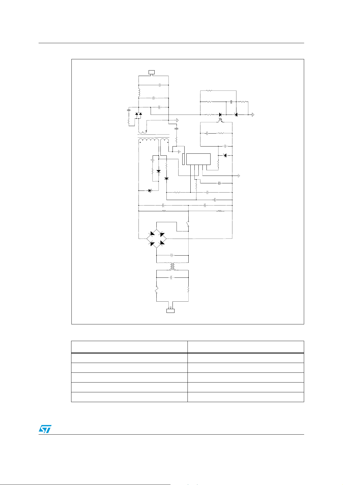
2 General circuit description
The power supply has been designed for the upper voltage range. The lower voltage range
utilizes a voltage doubler to raise the bulk voltage to 2 times the peak of the input line
voltage. In the doubling mode, the current charges one capacitor for each phase of the line,
therefore doubling the voltage. When SW1 is open, both capacitors are charged in series
resulting in a bulk voltage equal to the peak of the line input.
A wire jumper can be installed at production for units destined for countries using the lower
range. The switching frequency operates at 100 kHz. The output can deliver 18 V from no
load to 6 A continuous. The mode of operation ranges from discontinuous at high line
minimum load to continuous at low line max load. This mode of operation was chosen to
minimize the high peak currents of the discontinuous mode of operation.
The VIPer100A-E can be regulated in secondary mode with an optocoupler giving excellent
regulation or in the primary mode. Primary regulation works by regulating the V
output of the auxiliary winding. Depending on the coupling of the transformer, a 15%
regulation can be achieved. In this application, by taking advantage of the dual regulation, a
current limit scheme is obtained. This VIPer100A-E advantage, along with the transformer
design, constitutes the overcurrent circuit. The transformer is designed for a turn ratio of
operation for a universal input and an inductance to run in continuous conduction mode at
one-half the output load. The coupling between the secondary to auxiliary winding along
with the VIPer100A-E dual regulation plays an important part in the current limit.
pin at the
dd
Under typical operation, the output is tightly regulated through U2 and U3, the optocoupler
and TL431 respectively. As the output current increases, it causes the voltage at the
auxiliary output to increase. R4 is selected to trim the voltage at V
to reach 13 V when the
dd
output current exceeds the maximum limit. At this point, primary regulation takes over and
the output starts to fold-back.
The output uses an STMicroelectronics 100 V Schottky diode for better efficiency. C9 and
C10 are low ESR capacitors which manage the ripple current. U3 provides the reference
and the feedback to tightly regulate the output. C7, C8, and R6 form the feed back loop
compensation to optimize stability during transients.
Table 1. Electrical specification
Parameter Results
Input voltage 90-132 V
Output voltage J2
Load regulation (0.6 to 6 A) from set point +/- 0.6%
Line regulation (at max load) +/- 0.05%
Efficiency 86% @120 V
Output ripple voltage 15 mV max
Input power at no load 1.5 W typical
Transient response, 50% load step +/- 350 mV, +/- 1.9%, 200 µs settling time
with jumper in, 180 - 264 VAC no jumper
AC
and 87% @ 375 VDC
DC
EMI EN55022 and FCC class B
4/14
Page 5
AN1344 General circuit description
D3
STPS20H100C
T
C14
2.2nF
Y1 cap
R1
33
Thermistor
R14
470k
J2
CON2
1
2
D5
BZW50-180
C1
.1uF
X CAP
C4
100pF
1KV
Close for 120Vac
C2
330uF
200V
C20
330uf
200V
R9
1k
C6
4.7nF
50V
R8
10
R12
470k
C15
.1uF
50V
F2
FUSE
2.5A
5X20mm
J1
CON
123
123
C10
1800uF
25V
R5
4.22K
1%
R3
200
2W
BR1
600V 2A
BRIDGE
4 3
2
1
R11
20K
1%
C16
.001uf 1KV
R13
22 .5W
D1
STTA106
ST
600V
12
U2
H11A817A
1
2
4
3
D2
1N4148
12
SW1
SW SPST
1 2
18 V @ 6A
C7
22nF
50V
2 X 6mH
L1
2
1
4
3
R4
8.2
L4
10uH
C11
470uF
25V
R7
220
C12
.1uF
50V
C17
.1uF
X CAP
D4
NU
C8
1uF
50V
E34351E
TX1
Cramer Coil
2
394
7
5
.
...
.
.
C5
180uF
16V
U1
241
3
5
6
VDD
SOURCE
OSC
DRAIN
COMP
HS
U3
TL431
2
3
1
R10
3.16K
1%
R6
6.2K
C9
1800uF
25V
R0
0
R00
0 ohms
VIPer100A-E
Figure 2. Electrical schematic
Table 2. Transformer specification
Primary inductance 525 µH
Primary leakage inductance 7.9 µH
Inductance rating (al factor) 329 nH/T
Parameter Value
Core ETD34
Note Split primary - gapped core
5/14
Page 6

General circuit description AN1344
2.1 Transformer construction
Figure 3. Cross section of the transformer
The transformer is wound with a split primary to reduce leakage inductance and minimize
the snubbing needed. The auxiliary winding is placed on the outside to achieve the coupling
needed for the current limiting function.
Figure 4. PC board top legend and bottom foil (112 mm X 83 mm single sided)
6/14
Page 7

AN1344 General circuit description
Figure 5. Voltage and current waveforms
Figure 5 illustrates the voltage drain to source, and the current through the VIPer100A-E.
Vr3 is the V
across R3 to snub the diode. The maximum voltage drain to source
rms
measured 609 V out of the 700 V, specified maximum. The current shows the power supply
being in continuous conduction mode with a peak of 2 A. The snubber R3-C4 reduces
ringing thus lowering the maximum peak voltage on the Power MOSFET and reducing the
EMI. In these waveforms the transil, D3, was replaced by an RC clamp, (R2=39 K, 2 W and
C3=4700 pF). The clamp circuit worked the same under normal operation, but during start
up or during short circuit operation, the voltage on the drain of VIPer100A-E reached as high
as 750 V. The device is avalanche rugged and was able to withstand the momentary energy.
Using the Transil at this power level is preferred in order to reduce the stresses.
Table 3. Component list
Quantity Reference Value Part number
1 BR1 600 V, 1.5 A Bridge 2KBP06M
2 C1, C17 0.1 µF, X CAP P4610
2 C2, C20 330 µF, 200 V P6116
1 C4 100 pF, 1 KV P4116
1 C5 180 µF, 16 V P10245
1 C6 4.7 nF, 50 V P4793
1 C7 22 nF, 50 V P4517
1 C8 1 µF, 50 V P10312
1 C9 1800 µF, 25 V PANASONIC FC
1 C10 1800 µF, 25 V P10283
1 C11 470 µF, 25 V P6242C
2 C12, C15 0.1 µF, 50 V P4923
1 C14 2.2 nF, Y1 CAP P10463
7/14
Page 8

General circuit description AN1344
Table 3. Component list (continued)
Quantity Reference Value Part number
1 C16 0.001 µF, 1 KV P4128
1 D1 600 V STMicroelectronics STTA106
1 D2 1N4148
1 D3 2x10 A, 100 V STMicroelectronics STPS20H100CT
1 D4 3.3NZ NU
1 D5 STMicroelectronics BZW50-180
1 F2 2.5 A, 5x20 mm FUSE
1 J1 CON
1 J2 CON2
1 L1 2x6 mH PLK1084
1 L4 10 µH M6007
1 R0 0 WIRE
1 R00 0 Ω WIRE
1 R1 33 Ω Thermistor NW 96F3302
1 R3 200 Ω, 2 W
1 R4 8.2 Ω
1 R5 4.22 KΩ, 1%
1 R6 6.2 KΩ
1 R7 220 Ω
1 R8 10 Ω
1 R9 1 KΩ
1 R10 3.16 KΩ, 1%
1 R11 20 KΩ, 1%
2 R12, R14 470 KΩ, 1/4 W
1 R13 22 Ω, 1/2 W
1 SW1 SW SPST
1 TX1 Cramer Coil E34351E
1 U1 VIPer100A-E STMicroelectronics VIPer100A-E
1 U2 H11A817A
1 U3 TL431 STMicroelectronics TL431Z
8/14
Page 9

AN1344 Layout considerations
3 Layout considerations
Some simple rules to improve the performance and minimize noise should be followed:
1. Minimize power loops. Switched power current paths inner loop area must be as small
as possible. This can be achieved by careful layout of the printed circuit board. This
avoids radiated and conducted EMI noise, and improves efficiency by eliminating
parasitic inductance, thus reducing or eliminating the need for snubbers and EMI
filtering.
2. Use separate tracks for low level signal and power traces carrying fast switching pulses.
This can be seen on the VIPer100A-E pin 4. Ground is split between power and signal
traces on the printed circuit lay out. When signal paths share the same trace as a
power path, instabilities may result. The compensation components, C7, R6, and C9
are on a separate trace connected directly to the source of the device.
4 Burst mode
When the output current is too low, the minimum on time, fixed by the internal blanking time,
is too high to control the output voltage. In this case the burst mode operation takes over
automatically. The VIPer100A-E switch stays off when the voltage on the compensation pin
goes below 0.5 V. This results in missing cycles as shown in Figure 6. V
minimum output current is at 40 mA.
is 115 VAC,
in
Figure 6. Good burst mode
As can be seen, there is a burst of pulses followed by a pause of 600 ms. This repetitive
burst reduces power consumption while maintaining a negligible ripple on the output. The
V
voltage is stable, just above the low threshold of 8 V of the internal under voltage lock
dd
out. The under voltage lock out can be reached by further reducing the output current. As
the current decreases, the V
below the under voltage lock out of 8 V, another type of burst mode appears which is
controlled by the V
drawbacks, but the output voltage is still under control.
voltage. This is called “bad” burst mode (see Figure 7) because it has
dd
voltage on the primary side also decreases. When Vdd falls
dd
9/14
Page 10

Burst mode AN1344
Figure 7. Bad burst mode
At lighter load, the V
is reset, and the V
voltage drops below the under voltage threshold, the start up circuit
dd
capacitor charges back up to the high threshold of 11 V through the
dd
start up current source.
As shown in Figure 7 the reoccurrence of this cycle is about 300ms. The worst output
voltage swing is 2.4 V, which occurs at 20mA. At no-load condition, the output voltage swing
becomes negligible (45 mV).
This mode of operation leads to the following drawbacks:
1. Because the start up current source is turned on to supply the capacitor from a high
voltage rail, efficiency is dramatically reduced.
2. The recurring period leads to as much as 13% variation in the output voltage. For this
audio application it does not matter, but the designer should review all aspects of
operation.
3. Below the minimum current of 40 mA, the dynamic behavior is very poor which is
typical of all power supplies. If the demand of current occurs during the recharging
phase, the output capacitor is discharged and normal operation returns only at the next
starting phase.
In conclusion for this design a 40 mA minimum load is needed, 0.6% of maximum load, to
keep the unit in optimal performance. However, below this range, the output voltage is still
under control and no stresses are applied to the unit.
Table 4. Stand-by input power
Input voltage Input wattage at no-load Input wattage at 40 mA
90 V
0.85 W 1.77 W
ac
115 V
ac
132 V
1.3 W 1.86 W
ac
The transformer was optimized for the current scheme and not for Blue Angel.
10/14
1.1 W 1.8 W
Page 11

AN1344 Thermal consideration
5 Thermal consideration
Temperature measurement was taken at room ambient of 24 °C, convection air-cooled
resulted in the VIPer100A-E tab temperature of 91.1 °C at 115 V
input with a 6 A output.
ac
Results may vary depending on final application.
6 Overcurrent limiting
This power supply was designed for an audio application where music peaks can exceed
the maximum current of the power supply. In a sound entertainment system it is imperative
for the power supply to not shut down during such peaks. It is acceptable for the voltage to
decrease as the current increases. This maintains constant power for the unit. Under a short
circuit condition, this unit cycles on and off or "hiccup mode". In Figure 8 the output voltage
versus the output current is shown. Maximum output power reached is 163 W. The
VIPer100A-E also has thermal shutdown with hysteresis that is located close to the Power
MOSFET portion of the die, which protects it from exceeding the temperature limit of the I.C.
Figure 8. Output voltage versus the output
Figure 10. Output Ripple Figure 11. EMI measurement
current
Figure 9. Transient Response 50% step
change
11/14
Page 12

Transient response 50% step change AN1344
7 Transient response 50% step change
The output current is modulated from 3 A to 6 A, 50% duty cycle at a line input of 115 VAC.
The result is 322 mV or 1.8% dynamic regulation with a settling time of 500 microseconds.
8 Output ripple
The ripple was measured using an HP probe socket attached after the output connector.
This minimizes stray noise being picked up by the scope probe ground lead, which shows up
as high frequency noise.
The top trace shows the reduction in cost from eliminating L4 and C11. This gives a ripple,
at 6 A load, of 125 mV peak to peak. With the low pass filter the ripple is reduced to about
13 mV excluding voltage spikes.
9 EMI consideration
When dealing with EMI, it is always best to reduce noise at its source. Figure 11 shows FCC
class B plots comparing EMI at 6 amps load with snubber R3 and C4 in and out. The blue
trace, or lower trace, has the RC snubber across the diode. The EMI is reduced by 4 to 8 db.
Adding a 2W resistor and a capacitor here is much less expensive than adding across the
line capacitors and inductors in the EMI filter. This unit passed both EN55022 class B and
FCC class B.
10 Performance and cost consideration
This design has been optimized for performance. Cost can be reduced by substituting a 17V
zener for the TL431. The output regulation falls to the +/- 5% voltage set point, plus a
+0.084/°C temperature drift of the zener. The cost of the TL431 and 3 other passive
components can then be eliminated. If more output ripple voltage can be tolerated, than L4
and C11 can be eliminated.
11 Conclusion
This design delivers over 100 W for both voltage ranges by utilizing the VIPer100A-E with a
voltage doubler in the front end. The power supply has excellent regulation, current limiting,
short circuit protection, meets both EN55022 and FCC class B and best of all is from
STMicroelectronics.
12/14
Page 13

AN1344 Revision history
12 Revision history
Table 5. Document revision history
Date Revision Changes
04-Jan-2005 1 Minor text changes
18-Oct-2007 2
– Document reformatted no content change
– VIPer100A replaced by VIPer100A-E
13/14
Page 14

AN1344
Please Read Carefully:
Information in this document is provided solely in connection with ST products. STMicroelectronics NV and its subsidiaries (“ST”) reserve the
right to make changes, corrections, modifications or improvements, to this document, and the products and services described herein at any
time, without notice.
All ST products are sold pursuant to ST’s terms and conditions of sale.
Purchasers are solely responsible for the choice, selection and use of the ST products and services described herein, and ST assumes no
liability whatsoever relating to the choice, selection or use of the ST products and services described herein.
No license, express or implied, by estoppel or otherwise, to any intellectual property rights is granted under this document. If any part of this
document refers to any third party products or services it shall not be deemed a license grant by ST for the use of such third party products
or services, or any intellectual property contained therein or considered as a warranty covering the use in any manner whatsoever of such
third party products or services or any intellectual property contained therein.
UNLESS OTHERWISE SET FORTH IN ST’S TERMS AND CONDITIONS OF SALE ST DISCLAIMS ANY EXPRESS OR IMPLIED
WARRANTY WITH RESPECT TO THE USE AND/OR SALE OF ST PRODUCTS INCLUDING WITHOUT LIMITATION IMPLIED
WARRANTIES OF MERCHANTABILITY, FITNESS FOR A PARTICULAR PURPOSE (AND THEIR EQUIVALENTS UNDER THE LAWS
OF ANY JURISDICTION), OR INFRINGEMENT OF ANY PATENT, COPYRIGHT OR OTHER INTELLECTUAL PROPERTY RIGHT.
UNLESS EXPRESSLY APPROVED IN WRITING BY AN AUTHORIZED ST REPRESENTATIVE, ST PRODUCTS ARE NOT
RECOMMENDED, AUTHORIZED OR WARRANTED FOR USE IN MILITARY, AIR CRAFT, SPACE, LIFE SAVING, OR LIFE SUSTAINING
APPLICATIONS, NOR IN PRODUCTS OR SYSTEMS WHERE FAILURE OR MALFUNCTION MAY RESULT IN PERSONAL INJURY,
DEATH, OR SEVERE PROPERTY OR ENVIRONMENTAL DAMAGE. ST PRODUCTS WHICH ARE NOT SPECIFIED AS "AUTOMOTIVE
GRADE" MAY ONLY BE USED IN AUTOMOTIVE APPLICATIONS AT USER’S OWN RISK.
Resale of ST products with provisions different from the statements and/or technical features set forth in this document shall immediately void
any warranty granted by ST for the ST product or service described herein and shall not create or extend in any manner whatsoever, any
liability of ST.
ST and the ST logo are trademarks or registered trademarks of ST in various countries.
Information in this document supersedes and replaces all information previously supplied.
The ST logo is a registered trademark of STMicroelectronics. All other names are the property of their respective owners.
© 2007 STMicroelectronics - All rights reserved
STMicroelectronics group of companies
Australia - Belgium - Brazil - Canada - China - Czech Republic - Finland - France - Germany - Hong Kong - India - Israel - Italy - Japan -
Malaysia - Malta - Morocco - Singapore - Spain - Sweden - Switzerland - United Kingdom - United States of America
www.st.com
14/14
 Loading...