

Page 1
AN1336
APPLICATION NOTE
Power-Fail C omparator for
NVRAM Supervisory Devices
DEALING WITH UNEXPECTED POWER LOSS
Inadvertent or unexpected loss of power can cause a number of system level problems. Memory loss, uncontrolled program status and indeterminate processor state are just a few of the issues which can occur
during catastrophic power failure. Power-fail recovery is critical for applications created to perform machine control or instrumentation monitoring, therefore knowing the state of the operating system at the
time of power loss is very important.
The function of the Power Fail Comparator is to provide several milliseconds of early warning that power
is failing. This advance warning (see Figure 1) will allow a system to perform operations necessary to prepare for a controlled shutdown sequence. By using a special Power-Fail Input (PFI) to monitor the unregulated supply voltage, a Power Fail Output (PFO
Power-Fail Threshold (V
and to provide output power for a period of time after the input power to the power supply has failed. This
facility enables the power supply to ride through missing half cycles or missing cycles in an AC supply (see
Figure 2 on page 2).
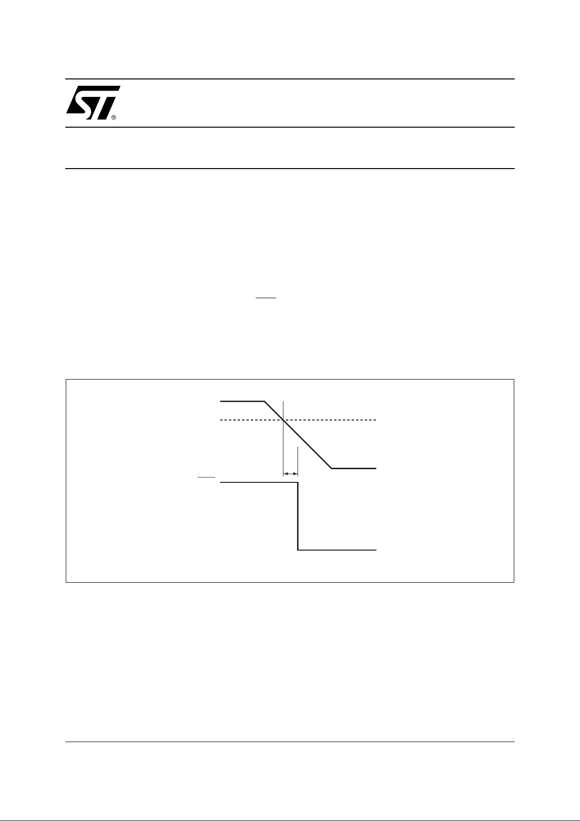
Figure 1. Powe r- Fai l Warning
). This is made possible by the ability of a power supply to continue to function
PFI
) can be generated t
after the supply f alls belo w t he
PFD
PFI
V
PFI
PFO
t
PFD
AI04224
1/9January 2001
Page 2
AN1336 - APPLICATION NOTE
Figure 2. Supply Hold-Up
AC Input
Regulated Output Voltage
Power-Fail Output
Power-Fail Warning
Supply Hold-up
AI04223
This is a result of the RC time constant inherent to most power supplies (see Figure 3). This time constant
is dominated by capacitors C
power-fa il, w hile C
and C1 will more directly affect the regu lat ed V cc slew r at e. Thus when t he A C input
3
and C3 (C2 is usually quite small). C1 will affect the V
1
slew rate during
UNREG
fails, this capacitance will continue to power t he circuit for several mil liseconds, typically on th e order of
10ms or more.
Figure 3. Typical Power Supply
V
UNREG
REGULATOR
C
C
1
2
C
3
V
CC
2/9
AI042222
Page 3
AN1336 - APPLICATION NOTE
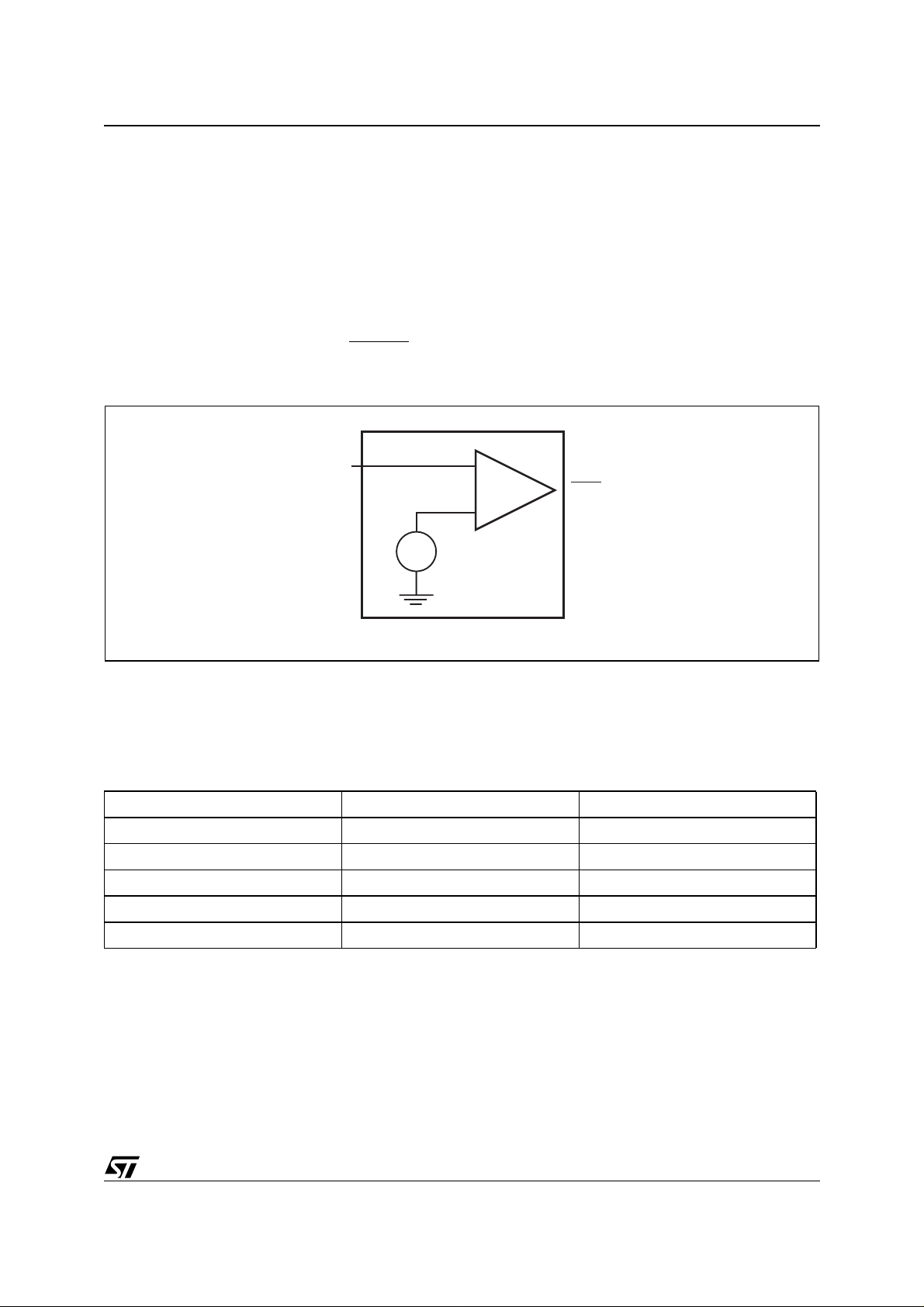
FUNCTIONAL DESCRIPTION
An independent bandgap reference comparator is used to monitor the unregulated supply voltage by connecting this supply to the Power-Fail Input pin. The RC time constant of the typical power supply will provide several milliseconds of operating voltage before decaying below a usable value. The Power-Fail Input
is constantly compared with an internal voltage reference of 1.25V (see Figure 4). If the input voltage falls
below 1.25V, the Power-Fail Output goes low. When it later goes above 1.25V, the output returns high.
Adding two external resistors (see Figure 5 on pa ge 4) as a v oltage d ivider circuit allows the comparat or
to supervise any voltage above 1.25V. The formula to calculate the trip point voltage of PFI (V
is dependent upon R1 and R2 is:
V
TRIP
PFI
=
R2
Where V
= 1.25V
PFI
V
(R1 + R2)
Figure 4. Powe r- Fai l Comparator C irc ui t
), wh i ch
PFI
PFI
1.25V
+
–
+
PFO
–
AI04221
The sum of both resistors should be about 1Mohm to minimize power consumption and to ensure the current in the PFI pin can be neglected compared with the current through the resistor network. The suggested resistor values are shown below (see Table 1). The tolerance of the resistors should not exceed 1% to
ensure the sensed voltage does not vary too much.
Tabl e 1. Look-up Table f or Diffe rent Tri p Points
R1 (kOhms) R2 (kOhms) Vtrip (V)
750 130 8.5
910 130 10.0
820 100 11.5
820 91 12.5
1100 100 15.0
3/9
Page 4

AN1336 - APPLICATION NOTE
PFI/PFO OPER ATION IN A SYSTEM (HOW DOES IT WORK?)
Figure 5. PFI/PFO in a Typical System
5V9V
Regulator
M41ST85Y
MCU SRAM
AC in
120/240V
50/60HZ
AC V
UNREG
V
PFI
R1
R2
V
V
IN
CC
V
V
CC
OUT
V
CC
V
CC
RST RST W
PFO
INT
NMI G
INT
E
PFI
E
CON
AI04220
A typical power failure can be described by the following three events (see Figure 6):
1. PFI Triggered (t
As V
UNREG
):
0
falls below the V
threshold, PFO is asserted on the MCU’s Non-maskable Interrupt (NMI)
PFI
pin. When NMI is asserted, the MCU halts its current task and begins saving critical data to the NVRAM
(safeguard routine).
2. V
begins to fall (t1):
CC
The MCU will continue f uncti oning unt il the safeguard routine is complete or RES ET
3. RESET
Asserted and/or Write Protect occurs (t2):
occurs.
At this point, the MCU needs to have completed the safeguard routine. This results in a safeguard window from PFI to RESET
/Write Protect (t2 - t0).
Figure 6. Power Failure Sequence
V
V
UNREG
PFI
V
CC
V
PFD
4/9
(t0) Power-Fail Input detected -
Begin Safeguard Routine
(t1) VCC begins to fall
(t2) Reset and/or Write Protect
Safeguard Window
t
t1t
0
2
(whichever occurs first)
t
AI04219
Page 5

AN1336 - APPLICATION NOTE
This safeguard window can be used for a number of purposes, depending on the application:
Power Save
The MCU can switch off, one by one, all non-critical peripheral compon ent s to conserve energy f or safeguard routines.
Data Transfer
The MCU may transfer data from the scratch pad memory to the Non-Volatile Memory. It takes only a few
MCU cycles if using NVRAM, but can take several milliseconds when this data needs to be stored in an
EEPROM or Flash memory.
Scratch Pad RAM Over-Write
Many applications are now required to run encode/decode algorithms (e.g. DES or RCA) for higher security. Therefore it is sometimes preferable to over-write the wo rking space be fore power-down to prevent
the contents of the RAM from being read illegitimately.
5/9
Page 6

AN1336 - APPLICATION NOTE
ADVANTAGES OVER TRADITIONAL POWER MONITORING
Typical power monitoring (or supervisory) devices of fer fea tures such a s brown-out det ect by mon itoring
the voltage at the V
may also include chip-enable gating or chip-enable write protection which will disable access to the memory, thereby protecting the SRAM contents from errant writes by an MCU that is operating in an undervoltage condition. These are good f eat ures and necessary to avoid catastrophic d ata loss, bu t unfortunat ely
do not occur early enough to allow the MCU to gracefully enter a fail-safe state. Any of the following scenarios will re s ult in un s atis f ac tory system shu t do wn:
Loss of Processor State
When the RESET occurs, any information not already stored to the NVRAM will be lost. This includes the
processor state, the program status, and any information still in the scratch pad RAM, but not in the
NVRAM.
RESET occurs during a write cycle
If the MCU is writing to memory when RESET occurs, that d at a wil l most likel y b e cor rupted. Thi s a p plies
to EEPROM and Flash memories as well as NVRAM.
Write Prote c t Occ ur s bef ore RESET
If the NVRAM gates off a ccess to the SRAM prior to proces sor RE SET , the process or m ay c ontinu e accessing/writing the NVRAM expecting that the data written is secure (when it has in fact, been lost).
pin, th en as serti ng a R ESET ou tput w hen VCC drops below a minimum level. Some
CC
6/9
Page 7

AN1336 - APPLICATION NOTE
HYSTERESIS
Hysteresis may be added to PFI for additional noise margin if desired (see Figure 7). The ratio of R1 and
R2 should be selected such that PFI sees V
between PFI and PFO
provides the hysteresis and should typically be more than 10 times the value of R1
or R2. The hysteresis window will extend both above (V
Figure 7. Adding Hysteresis
V
IN
when V
PFI
falls to its trip point (V
UNREG
) and below (VL) the original trip point.
H
PFO
TRIP
). Connecting R3
R1
V
CC
GND
R2
PFI
R3
C1
PFO
TO
CONTROLLER
Connecting an ordinary signal diode in series with R3 (see Fi gure 8) so the lower trip point (V
cides with the trip point without h ysteresis, causing the entire hys teresis window to occur abo ve V
0V
0V
V
= V
TRIP
VH =
VL = R1
where
V
PFI
V
PFH
PFI
V
()R1()
PFI + VPFH
V
[]
PFI
= 1.25V
= 10mV
V
V
L
TRIP
R1 + R2
()
R2
1 + 1 + 1
()
R1
R2
V
H
1 + 1 + 1
()
R2 R3
R1
V
CC
–
R3
R3
AI03077
L
V
IN
) to coin-
TRIP
This method provides additional noise margin without compromising the accuracy of the power-fail thresh-
old when the monitored voltage is falling. The current through R1 and R2 should be at least 1µA to ensure
that the 25nA PFI input current does not shift the trip point. The capacitor C1 is added for noise rejection
and should be quite small (e.g., ~100nF), but is optional.
Figure 8. Hysteresis on Rising V
V
IN
IN
PFO
.
R1
R3R2
C1
TO
CONTROLLER
PFI
PFO
V
CC
GND
0V
0V
V
= V
TRIP
VH = R1 V
where
V
= 1.25V
PFI
V
= 10mV
PFH
VD = Diode Forward Voltage Drop
V
TRIP
R1 + R2
()
PFI
R2
()
[]
PFI + VPFH
()
R1
V
1 + 1 + 1
R2 R3
H
V
D
–
R3
AI03076
V
IN
7/9
Page 8

AN1336 - APPLICATION NOTE
Table 2. SUPERVISORY ZEROPOWER/TIMEKEEPER® Products with Power-Fail Comparator
Category Devices
ZEROPOWER (SZ) M40SZ100Y, M40SZ100W
TIMEKEEPER (ST) M48ST59Y/V/W, M48ST37Y/V/W, M41ST85Y/W, M41ST84Y/W
CONTACT INFORMATION
If you have any questions or suggestions concerning the matters raised in this document, please send
them to the following electronic mail addresses:
apps.nvram@st.com
ask.memory@st.com
(for application support)
(for general inquiries)
Please remember to include your name, company, location, telephone num ber, and fax number.
8/9
Page 9

AN1336 - APPLICATION NOTE
Information furnishe d is bel i eved to be accurate and reliable. However, STMicroelectro ni cs assumes no responsibility for t he consequences
of use of such information nor for any infringement of patents or other rights of third parties which may result from its use. No license is granted
by implic ation or oth erwise unde r any patent or patent rights of S TMicroelec tr onics. Specification s mentioned in this publication are subj ect
to change without notice. This publication supersedes and replaces all information previously supplied. STMicroelectronics product s are not
authorized for use as critical components in life su pport devices or systems wit hout express wri tten approv al of STMicroelectronics.
The ST log o i s registered trademark of STM i croelect ronics
All other names are the property of the i r respectiv e owners.
© 2001 STMicroelectronics - All Rights Reserved
Australi a - Brazil - China - Finland - F rance - Germany - Hong Kong - India - Italy - Japan - Malaysi a - M al ta - Morocc o -
Singapor e - Spain - Swede n - Switzerla nd - United Kingdom - U.S.A.
STMicroelect ro n ics GRO UP OF COMPANI ES
www.st.c o m
9/9
 Loading...