

Page 1

AN1335
APPLICATION NOTE
Using the ST10F280
By André ROGER
1 - INTRODUCTION
ST10F280 is a new member of ST10 family. This device has been specifically designed for application
based on C167 an d that now requires signal processing: a timer has been added for signal sampling
(automatic triggering of ADC requests on a pre-defined time period).
This application note is showing how to design an application using ST10F280. The following aspects are
covered and detailed :
– Emulation,
– Porting from ST10F269,
– Peripheral configuration.
1/10April 2001
Page 2

AN1335 - APPLICATION NOTE
TABLE CONTENTS PAGE
1 INTRODUCTION ........................................................................................................ 1
2 ST10F280 NEW FEATURES FULLY SUPPORTED BY EMULATOR S ................... 3
2.1 XPORT9...................................................................................................................... 3
2.2 XPORT10.................................................................................................................... 3
2.3 XTIMER....................................................................................................................... 3
2.4 XPWM ......................................................................................................................... 3
3 ST10F280 REGISTERS NOT SUPPOR TED BY THE EMULATO R ......................... 3
3.1 SOFTWARE ADVICE FOR NOT IMPLEMENTED REGISTERS................................ 3
3.2 PORT4 REGISTERS................................................................................................... 3
3.3 PORT5 REGISTERS................................................................................................... 4
3.4 POCON REGISTERS.................................................................................................. 4
3.5 XPERCON REGISTER............................................................................................... 4
3.6 EXISEL REGISTER..................................................................................................... 4
4 ST10F280 REGISTERS PARTLY SUPPORTED BY THE EMULATOR ................... 5
4.1 PICON REGISTER...................................................................................................... 5
4.2 WDTCON REGISTER................................................................................................ 5
5 ST10F280 PERIPHERALS NOT SUPPORTED BY THE EMULATORS .................. 5
5.1 ST10F280 FLAS H ....................................................................................................... 5
5.2 BOOSTRAP................................................................................................................. 5
6 DC/AC PARAMETER DIFFERENCES ............. ......... .......................... .......... ......... ... 6
7 PORTING AN APPLICATION FROM ST10F269 TO ST10F2 80 .............................. 6
7.1 DIFFERENCES IN PERIPHERAL SET....................................................................... 6
7.2 DIFFERENCES IN MEMORY MAPPING.................................................................... 6
7.2.1 Differences on the RAM ............................................................................................. 6
7.2.1.1 Differences in Flash..................................................................................................... 6
8 ST10F280 PERIPHERAL CONFIGURATION ........................................................... 6
8.1 XPORT9...................................................................................................................... 6
8.2 XPORT10.................................................................................................................... 6
8.2.1 ADC Software Driver Considerations ......................................................................... 7
8.3 XTIMER....................................................................................................................... 7
8.3.1 Manual Injection Convers ion Reque st ........................................................................ 7
8.3.2 Proposal of ADC Driver When Converting All Channels Regularly ............................ 7
8.3.3 Example ...................................................................................................................... 7
8.3.3.1 Software Configuration................................................................................................ 8
8.3.3.2 Hardware Configuration............................................................................................... 8
8.4 XPWM ......................................................................................................................... 8
8.4.1 Bit Addressability and Interrupt Requests .................................................................. 9
8.4.2 XPWM Software Advice Summary ............................................................................. 9
9 APPLICATION NOTE VERSION INFORMATION ..................................................... 9
9.1 REVISION OF 29TH OF APRIL 2001 ......................................................................... 9
2/10
Page 3

AN1335 - APPLICAT ION NOTE
2 - ST10F280 NEW FEATURES FULLY SUPPORTED BY EMULATORS
This paragraph describes the features that are fully supported by the ST10F280 emulator.
2.1 - XPort9
XPort9 and its associated features can be fully supported by the emulators.
Note: XPort9 register9 is not addressable as a standard ST10 port register; care should be taken when
accessing the Xport9 registers. For simplicity, 2 registers have been added : one to set and
another one to clear specific pins.
2.2 - XPort10
Xport 10 and the associated 16 new ADC analog channel s can be fully supported by the emulator.
XP10DISDIS, is also fully supported (this is not the case for P5DIDIS; see Section 3.3 - Port5 Registers).
2.3 - XTimer
Xtimer, which allows to activate an external pin, which in the end can t ri gger an A DC conversion request
can also be fully suppor ted by the emulator.
2.4 - XPWM
XPWM, and its ass ociated features are fully suppor ted by the e mulators. Alltough those PWM channels
are identical to the one of other ST1 0 variants, users are advised to check the chapter des cribing F280
peripheral configuration.
3 - ST10F280 REGISTERS NOT SUPPORTED BY THE EMULATOR
This paragraph describes all the issues caused by ST10F280 registers that are not implem ented in the
emulator.
3.1 - Software Advice for not Implemented Registers
When a ST10F280 register is not implemented in the bond-out :
– Avoid unnecessary read and c heck of the value in this register,
– If read accesses in user mode are necessary, use the CPU IDCHIP register to detect which CPU is run-
ning the code. Then, allow the check on this register only for the ST10F280. If running from the
bond-out, use a pre-defined, but non initialised, memory variab le to set which configuration you want
during emulation.
3.2 - Port4 Registers
Description
ST10F280 register OD P4 is not implemen ted on the ST1 0 bond-out. T his register allows setting t he pin
that handles CAN-TX alternate functions in push-pull or in open-drain.
Software Impact
Application software only shall write to this register.
Hardware Impact
No hardware impact if ST advices are implemented by the emulator party (check with your emulator
supplier).
ST10F280 Emulation Impact
No impact if ST advi ces are implemented and if t he content of the register is fixed at initialisation (ie :
never changed during run time) and if the emulator is properly configured.
3/10
Page 4

AN1335 - APPLICATION NOTE
3.3 - Port5 Registers
Description
ST10F280 regis ter P5DIDIS is not implemented in the emulator. This register is used to enhan ce the
accuracy on analog inputs within the temperature and supply voltage range.
Software Impact
Application software only shall write to this register.
ST10F280 Emulation Impact
No impact if software recommandations are used.
3.4 - POCON Registers
Description
Those registers are not implemented in the emulator, but are implemented in the ST10F280. They allow
to set the rise/fall time and the output current characteristics of the I/O ports.
Software Impact
Application software only shall write to this register.
Hardware Impact
The I/O ports characteristics are fixed to the one of the ST10 bond-out : fast edge and high current.
ST10F280 Emulation Impact
If those modes are only used to minimize EMC, there is no impact on ST10F280 emulation.
3.5 - XPERCON Register
Description
This register is not im plemented in the e mulator, but is implemented in the S T10F280. The em ulator
Xperipherals are enabled by the user in the emulator environment.
Software Impact
Application software only shall write to this register.
ST10F280 Emulation Impact
No impact if software recommandations are used and if the emulator is properly configured.
3.6 - EXISEL Register
Description
This register is not i mp lem ented in the emulator, but is implemented in t he ST10F280. It allows to select
the source for the fast interrupt (pin from Port2 or/and ST10F280 specific alternate function).
Software Impact
Application software only shall write to this register.
Hardware Impact
No hardware impact if ST advices are implemented by the emulator party (check with your emulator
supplier) : static configuration of the emulator can replace EXISEL.
ST10F280 Emulation Impact
No impact if ST advices are implemented, if the con tent of the register is fixed at initialisation (ie : never
changed during run tim e) and if the emulator is properly configured.
4/10
Page 5

AN1335 - APPLICAT ION NOTE
4 - ST10F280 REGISTERS PARTLY SUPPORT E D BY THE EMULATOR
This paragraph describes all the issues caused by ST10F280 registers that are implemented in the
emulator but in a different way than the ST10F280 (new bits added or modified bit functionality).
4.1 - PICON Register
Description
Bit4 (P4LIN) is not implemented on the ST10 bond-out.
Software Impact
Application software only shall write to this register.
Hardware Impact
Hystereris cannot be implement ed on P4 during emulati on.
ST10F280 Emulation Impact
As usual, hysterersis is used to minimise noise effects, the impact on the application is minimized.
4.2 - WDTCON Register
Description
This register is implemented in the ST10 bond-out chip but all the bits that allow to identify the reset cause
are not implemented.
Software Impact
The cause of the reset cannot by dynamically emulated.
ST10F280 Emulation Impact
To allow to similate a reset cause, it is proposed :
the reset procedure shall be written in a way to detect which silicon is running the software : ST10F280 or
the Bond-out (via IDCHIP register). Then, when running c ode from the bond-out, it is proposed to use a
non initialised variable (initialised by the user before running emulation) to check the reset cause.
5 - ST10F280 PERIPHERALS NOT SUPPORTED BY THE EMULATORS
This paragraph describes all issues caused by peripherals that are not supported by the ST10 emulators.
5.1 - ST10F280 Flash
Description
In emulation, the bond-out is running code from RAM mapped into the ST10 bond-out memory space.
ST10F280 Emulation Impacts
– The automatic remappi ng of the fla sh in normal m ode or bootst rap mode will not be su pported => to
have one software for each memory mapping.
– Some of the Flash specific features are not supported (Flash programmi ng commands are not rec og-
nised, reading any Flash registers will lead to undefined content).
5.2 - Boostrap
Description
ST10F280 bootstrap mode cannot be supported as it is by the emulator. ST10F280 automatically
activates the boot-Flash and remaps some memory blocks if boot-strap mode is selected. ST10
bond-outs cannot do that. This limitation is not specific to ST10F280.
ST10F280 Emulation Impacts
To debug the bootstrap software routines, u sers will nee d t o have a spe cific software for this mode. T his
specific software, loaded into the emulator memory, shall have all the software inside the boot-Flash and
all the needed software from the other blocks of the Flash.
5/10
Page 6

AN1335 - APPLICATION NOTE
6 - DC/AC PARAMETER DIFFERENCES
Allthough minimized as far as possible, there will be differences in DC and AC parameters.
For detailled differences on DC or AC parameters, please refer to the latest ST10F280 datasheet.
7 - PORTING AN APPLICATION FROM ST10F269 TO ST10F280
ST10F269 and ST10F280 are both members of ST10 familly and, as a consequence are compatible.
Due to differences in per ipheral set and in mem ory mappi ng, there are few differences that need to be
considered to por t an application from ST10F269 to ST10F280.
7.1 - Differences in Peripheral Set
Added Xperipherals : XPort9, Xpor t10 with 16 new ADC channels, XPWM, XTimer.
Removed Peripherals: real time clock (RTC).
The peripheral set differences require changes in the initialisation of XPERCON register.
If the RTC is not used, this is the only change to do, to take into account the differences of peripherals.
7.2 - Differences in Memory Mapping
7.2.1 - Differences on the RAM
The RAM on Xbus is changed from 10K Bytes to 16K Bytes. The address range is changed from
00’C000h/00’E7FFh to 00’8000h/00’BFFFh.
This change requires:
– An update of the link parameters,
– A DPP to be allocated to the part of the XRAM page2 memory address,
– A modification of the value written in XPERCON register (F269 has 2 bits to control XRAM; F280 has only 1).
7.2.1.1 - Differences in Flash
The Flash is increased from 256K Bytes to 512K Bytes.
– Programm ing model is unchanged,
– Flash memory ma pping is unchange d on the first 256K Bytes part of ST10F280 Flash.
The only modification is that it is no longer possible to pull the Flash status using XP2IR interrupt flag.
Pulling shall be done using the Flash status register (already available with ST10F269).
8 - ST10F280 PERIPHERAL CONFIGURATION
This part of the technical note is giving advice on the configuration to have or to avoid with ST10F280.
8.1 - XPort9
XPort9 and its associated features can be fully supported by the emulators.
Due to emulation constraints, it was not possible to map XPORT9 in the bit addressable area, each of the
XPort9 registers that may need to be changed after CPU initialisation has been split into :
– 1 set register : used to set specified bits (writting a 0 has no effect)
– 1 clear register : used to clear specific bits (writting a 0 has no effect).
Software shall use those registers depending on what value is intended on the output pins (or other
registers).
8.2 - XPort10
Allthough Xport10 and the associated 16 new ADC analog channels can be fully supported by the
emulator, there is no way in the ADC conversion results register to identify which part of the 32 channels
has been converted : low part of the 32 channels (ie : Port5) or high part (ie : Xport10).
6/10
Page 7

AN1335 - APPLICAT ION NOTE
8.2.1 - ADC Software Driver Considerations
The handling of bit XADCMUX shall be done preferably by a unique piece of software.
If ADC automatic scan is used (with or without PECC) to fill-up a table of conversion channels, it shall be
the software driver responsibility to handle this bit and generate the correct address to write to this table).
8.3 - XTimer
Xtimer, which allows to activate an external pin, which in the end can t ri gger an A DC conversion request
can also be fully suppor ted by the emulator.
Allthough it is fully supported, some c are is necessar y :
The conversion-injection-request will be triggered without knowing the value of bit XADCMUX.
Practically , in engine control application, this bit may change dynamically and ensuring a predefined value
during injection request may be difficult.
As a result, it is advised to duplicate to 2 analog channels the analog signal to compare on inj ection
request.
Note: It is better to allocate P5.15 and P10.15 to the channel to convert on injection request : this allow
to optimise the number of channels to scan during the auto-scan of the ADC channels.
8.3.1 - Manual Injection Conversion Request
Injection conversions can be initiated by software rather than Xtimer. This feature is already existing on
ST10 and requires to write to bit INJ_REQ in ADCON register.
8.3.2 - Proposal of ADC Driver When Converting All Channels Regularly
This proposal is showing how to configure ST10F280 when scanning regularl y all channels and storing
conversion results with PECC :
ADC scan start routine : unchanged
PECC : end-of-count interrupt routine :
– Must be changed to distinguish between 1st half of scan and second half of scan (new variable needed).
– To summarize :
– Check bit XADCMUX,
– If 1st half (assume XADCMUX=0), change bit XADCMUX, start another scan,
– If 2nd half : re-init PECC for xx channels (1 to 16), change bit XADCMUX.
– Here, we assume that ADC scan are initiated by another routine (either timer based, ...).
ADC + PECC init routine : to allow more room for the table of conversion results.
8.3.3 - Example
The example hereafter illustrates how to generate of X_ADC_INJ output for the channel injection mode of
the A/D converter. It both describes the software and hardware configurations. XTIMER is used as a
counter that is clocked with XCLK divided by 8 and that counts from 0 (start value) to F (end value). It is
configured with "continue" and "reload start value" mode.
7/10
Page 8
AN1335 - APPLICATION NOTE
8.3.3.1 - Software Configuration
; init XTCR
MOV R3, #0C000h ;XTCR address
MOV R0, #009Eh ;configuration value
MOV [R3], R0
; init TSVR
MOV R3, #0C002h ;register address
MOV R0, #0000h ;start value
MOV [R3], R0
; init TEVR
MOV R3, #0C004h ;register address
MOV R0, #000Fh ;end value
MOV [R3], R0
; run Xtimer by XTCR
MOV R3, #0C000h
MOV R0, #009Fh
MOV [R3], R0
Note : bit : "interrupt enable" in XTCR shall be set to enable th esignal on Xtimer output pin (X_ADC_INJ).
8.3.3.2 - Hardware Configuration
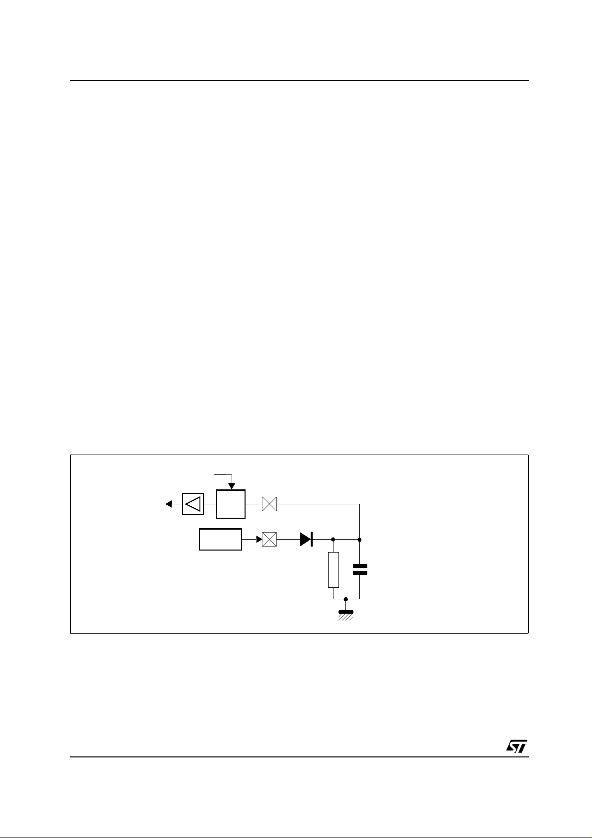
In practic e, the falling edge of the X_ADC _INJ signal mus t be delayed up to 8 CPU clock cycle s. The
following figure shows the external circuit that have to be added:
Figure 1 : External Connection for ADC Channel Injection
Clock
P7.7/CC31
CAPCOM2 UNIT
Input
Latch
XTIMER
X_ADC_INJ
Output trigger for ADC
channel injection
Typical value:
CR
R = 10KΩ C = 47pF at 40MHz
8.4 - XPWM
XPWM are identical to the one in ST10 peripheral address range.
The differences to the user are due to the fact they are not bit addressable and that all the associated
interrupt requests have been ORed on a single interrupt node.
8/10
Page 9

AN1335 - APPLICAT ION NOTE
8.4.1 - Bit Addressability and Interrupt Requests
XPWMCON 0 and XPWMCON1 registers are not bit addressable and register XPWMCON0 has all the
interrupt request flags.
To avoid to loose interrupt requests, it is necessary to stop all the PWMs before changing the
XPWMCON0 register.
Changes in XPWMCON0 must ensure coherency (ie : uninterruptible read-modify-write sequence).
To make an instruction sequence uninterruptible, use ATOMIC instruction before the sequence.
8.4.2 - XPWM Software Advice Summary
– Stop all PWMs before changing XPWM CONx regist ers
– Change them using uninterrup tible sequence (u se ST10 AT OM IC #xx instruction).
– Re-enable PWM that were running as soon as changes are done to avoid increase in inaccuracy of the
PWM outputs.
9 - APPLICATION NOTE VERSION INFORMATION
9.1 - Revision of 29th of April 2001
This is the first version of AN1335.
9/10
Page 10

AN1335 - APPLICATION NOTE
Information furnished is bel ieved to be accurate and reliable. However, STMicroe lectronics assumes no responsibility for the
consequences of use of such information nor for any infringement of patents or other rights of third parties which may result from
its use. No li cense is granted by implication or otherwise unde r any patent or patent rights of STMicroelectronics. Specifications
mentioned in this publication ar e subject to change without notice. This publication supersedes and replaces all information
previously supplied. S TMicroelectronics products are not authorized for use as critica l components in life suppo rt devices or
systems without express written approval of STMicroelectronics.
The ST logo is a registered trademark of STMicroelectronics
© 2001 STMicroelectronics - All Rights Reserved
STMicroele ct ronics GROUP OF COM PANIES
Australi a - Brazil - Chi na - Finlan d - F rance - Germany - Hong Kong - India - Ital y - Japan - Ma l aysia - Malta - Morocco
Singapo re - Spain - Sweden - Swit zerland - Un i ted Kingdom - U.S.A.
http://www.st.com
10/10
 Loading...