

Page 1

AN1334
APPLICATION NOTE
ST10F269/F280 System Reset
By André ROGER
1 - INTRODUCTION
This application note is intended for hardware designers. It explains the different kinds of reset available
on ST10F269/ST10F280 and compares ST10F269/ST10F280 reset features with ST10F168 ones.
More specifically, after a quick summar y, it details the new flags added to WDTCON register, then gives
an application view of the different resets. A specific chapter is devoted to the bidirectional reset to detail
the advantages and constraints of using this mode.
After des c ribing the start-up c on f igu ra ti on , us er s will find a chapter de t ailing ST10 res et key param e t er s.
1/18February 2001
Page 2

AN1334 - APPLICATION NOTE
TABLE CONTENTS PAGE
1 INTRODUCTION......................................................................................................... 1
2 SYSTEM RESET......................................................................................................... 3
3 WDTCON NEW FLAGS FOR RESET CAUSES........................................................ 5
3.1 WDTCON DESCRIPTION........................................................................................... 5
3.2 POWER-ON DETECTION........................................................................................... 5
3.3 SUPPLY MONITORING.............................................................................................. 6
4 RSTOUT PIN............................................................................................................... 6
5 RESET AND RPD PIN ................................................................................................ 6
6 APPLICATION VIEW.................................................................................................. 8
6.1 POWER-ON HARDWARE RESET ............................................................................. 8
6.2 POWER-ON RESET AFTER A PARTIAL POWER FAILURE .................................... 8
6.3 LONG HARDWARE RESET ....................................................................................... 9
6.4 SHORT HARDWARE RESET..................................................................................... 9
6.5 SOFTWARE RESET................................................................................................... 10
6.6 WATCHDOG TIMER RESET...................................................................................... 11
7 BI-DIRECTIONAL RESET.......................................................................................... 11
7.1 BI-DIRECTIONAL RESET AND RSTIN CHARGE TIME ............................................ 12
7.2 BI-DIRECTIONAL RESET AND SHORT HARDWARE RESET.................................. 13
8 SYSTEM START-UP CONFIGURATION ................................................................... 13
9 RESET KEY PARAMETERS...................................................................................... 15
9.1 RSTIN ACTIVATION TIME.......................................................................................... 15
9.1.1 Power-on Reset Time.................................................................................................. 15
9.1.2 Asynchronous Reset................................................................................................... 15
9.1.3 Software or Watchdog Reset....................................................................................... 15
9.2 CONFIGURATION RESISTORS ON PORT0............................................................. 15
9.2.1 Pull-down Resistors..................................................................................................... 15
9.2.2 Pull-up Resistors ......................................................................................................... 15
9.2.3 PLL Lock Sequen ce, Configuration Resistors and Reset Duration............................. 15
9.3 COMPONENTS ON RPD PIN ..................................................................................... 16
9.3.1 Difference with ST10F168........................................................................................... 16
9.3.2 Interruptible Power-down Mode Not Used................................................................... 16
9.3.3 Interruptible Mode is Used........................................................................................... 16
10 APPLICATION NOTE VERSION INFORMATION...................................................... 16
10.1 REVISION OF 5TH OF FEBRUARY 2001.................................................................. 16
2/18
Page 3

AN1334 - APPLICAT ION NOTE
2 - SYSTEM RESET
System reset initializes a device into a pre-defined default state.
ST10F269 and ST10F280 h ave the same types of reset as ST10F16 8
– Asynchronous hardware reset : defined by assertion of the RSTIN
– Synchronous short hardware reset: defined by assertion of the RSTIN
level on RPD pin.
– Synchronous long hardware reset: defined by assertion of the RSTIN
high level on RPD pin.
– Software reset: reset initiated by the execution of SRST instruction.
– Watchdog reset: reset triggered by an overflow of the watchdog timer.
The functionalities associated to reset are unchan ge d
– Bidirectional reset can be enabled to convert software and watchdog resets to hardware reset.
– RSTOUT
is activated once reset conditions are detected and rema ins active until the execution o f the
EINIT instruction. The CPU and peripherals are set in their predefined default state.
– The content of some sp ecial fun ction re gister s (SYSCON, BUSCO N0, RP0H) ar e control led duri ng sys-
tem start-up configuration via PORT0 pins. The sy stem start-up configuration is sampled differently
upon the different reset types.
– After the internal reset condition is removed, the microcontroller will start program execution from mem-
ory location 00’0000h in code segment zero. This start location will typically hold a branch instruction to
the start of a software initialization routine for the application specific configuration of peripherals and
CPU Special Function Registers.
pin with a low level on RPD pin.
pin for less 1032 TCL, with a high
pin more than 1032 TCL, with a
Difference with ST10F168
The main difference with ST10F168 is that register W DTCON has been modified to suppor t 1 flag per
reset source to indicate the reset cause.
3/18
Page 4
AN1334 - APPLICATION NOTE
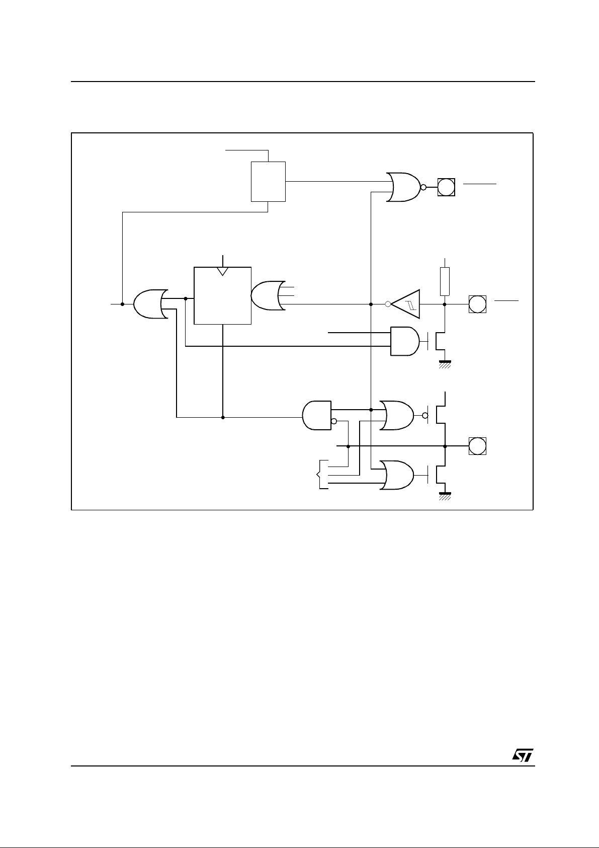
ST10F269 and ST10F280 internal reset circuitry is the following:
Figure 1 : Internal Reset Circuitry
EINIT Instruction
Clr
Q
Set
Reset State
Machine
Clock
RSTOUT
V
CC
Internal
Reset
Signal
Trigger
Clr
Reset Seq uen ce
(512 CPU Clock Cycles)
Asynchronous
Reset
From/to Exit
Powerdown
Circuit
SRST instruction
watchdog overflow
BDRSTEN
V
CC
Weak pull-down
(~200
RSTIN
RPD
µ
A)
Note: ST10F269 and ST10F 280 internal reset circuitr y is the same as ST10 F168 except that VPP pin
is used only for the timing control during "Return from Powerdown" and to select the type of reset:
asynchronous or synchronous type of reset. Pin 84 name is now "RPD" .
4/18
Page 5

AN1334 - APPLICAT ION NOTE
3 - WDTCON NEW FLAGS FOR RESET CAUSES
3.1 - WDTCON Desc rip tion
Compared to ST 10F168, ST10 F269 and ST10 F280 WDTC ON registers have been modified t o indicate
the cause of the reset:
Each of the different reset sources is now indicated in the WDTCON register. The indicated bits are
cleared with the EINIT instruction. It is thus possible to identify the reset during the initialisation phase.
WDTCON (FFAEh / D7h) SFR Reset Value: 00XXh
1514131211109876543210
WDTREL - - PONR LHWR SHWR SWR WDTR WDTIN
RW HR HR HR HR HR RW
WDTIN Watchdog Timer Input Frequency Selection
‘0’: Input Frequency is f
‘1’: Input Frequency is f
1 - 3
WDTR
1-3
SWR
1-3
SHWR
1-3
LHWR
1- 2-3
PONR
Notes: 1. More tha n one reset indication flag may be set. After EINIT, all flags are clear ed.
2. Power-on is dete ct ed when a risi ng edge from V cc = 0V to Vcc > 2.0V i s recognized on the inter nal 3.3V supply.
3. Those bits cannot be directly modified by software...
Watchdog Timer Reset Indication Flag
Set by the watchdog timer on an overflow.
Cleared by a hardware reset or by the SRVWDT instruction.
Software Reset Indication Flag
Set by the SRST execution.
Cleared by the EINIT instruction.
Short Hardware Reset Indication Flag
Set by the input
Cleared by the EINIT instruction.
Long Hardware Reset Indication Flag
Set by the input RSTIN
Cleared by the EINIT instruction.
Power-On (Asynchronous) Reset Indication Flag
Set by the input RSTIN
Cleared by the EINIT instruction.
RSTIN.
/2.
CPU
/128.
CPU
.
if a power-on condition has been detected.
3.2 - Power-on Detection
ST10F269 and ST10F280 have power-on detection circuitry .
The PONR flag of WDTCON register is set if the output voltage of the internal 3.3V supply falls below the
threshold (typically 2V) of the power-on detection circuit. This circuit is efficient to detect major failures of
the external 5V supply but if the internal 3.3V supply does not drop under 2 volts, the PONR flag is not
set. This coul d be the case on fast switch-off / switch-on of the 5V supply. The time need ed for such a
sequence to activate the PONR flag depends on the value of the capacitors connected to the supply and
on the exact value of the internal threshold of the detection circuit.
5/18
Page 6

AN1334 - APPLICATION NOTE
3.3 - S u pply Monitorin g
ST10F269 and ST10F280 have on-chip power-on detection circuitry. This circuitry is detecting major
failure on the supply and will not generate a reset when the external supply is going out of ST10 circuit
specification (either marginally, either for a very short period).
As a consequence, when an exter nal supply monitoring circuit is used, the ta ble of WDTCO N af ter reset
becomes:
The following table is showing the value of WDTCON bits for the 6 possible causes of reset:
Reset Source PONR LHWR SHWR SWR WDTR
Power-on Reset (all bit are set) X X X X
Power-on after Partial Supply Failure * X X X
Long Hardware Reset X X X
Short Hardwar e Reset X X
Software Reset (only SWR bit is set) X
Watchdog Reset XX
* P O NR bit may not be s et for sh ort supply failure.
For Power on reset aft er supply partial failure, asynchronous res e t mu st be used.
In case bi-di rectional reset is enabl ed, and if the RSTIN
reset, a software reset or a watchdog reset will trigger a Long hardware reset. Thus, Reset Indications flags will be set to indicate a Long
Hardware Rese t.
pin is latched l ow after the end of internal reset sequen ce, then a Shor t hardware
4 - RSTOUT PIN
The behaviour or RSTOUT
The RSTOUT
pin is dedicated to generate a reset signal for the system components besides the
pin of ST10F269 and ST10F280 is identical to ST10168:
controller itself.
RSTOUT
For synchronous reset, as the CPU is completing its current bus cycle, RSTOUT
pin is activated once reset conditions are detected.
may be activated before
the internal CPU reset sequence is star ted.
RSTOUT
remains activated until the execution of the EINIT instruction. This allows the complete
configuration of the controller including its on-chip peripheral units before releasing the reset signal for the
external peripherals of the system.
RSTOUT
pulses on RSTOUT
will float as long as pins P0L.0 and POL.1 selec t emulation mode or adapt mode ; to avoid
P0L.0 and P0L.1 are latched at the end of the reset sequence (see diagrams showing
sampling point of PORT0 pins).
5 - RESET AND RPD PIN
As explained before, the level on pin RPD (pin 84) defines the reset type when RSTIN
– Asynchronous reset: defined by assertion of the RSTIN
– Synchronou s reset: defined by assertion of the RSTIN
pin with a low level on RPD pin.
pin with a high level on RPD pin.
is activated:
Then, if RPD is pulled low in synchronous reset, the chip immediatly enters in asynchronous reset.
Synchronous Reset
Advantage: this reset shall be used when short pulses on RSTIN
pin can be applied to generate a circuit
reset during circuit operation.
6/18
Page 7

AN1334 - APPLICAT ION NOTE
Disadvantage: reset effect on circuit may be delayed up to 2 CPU clock cycles (sampling time) and th en
by another period to leave the CPU to complete the current internal bus cycle.
Figure 2 : Long Synchronous Reset Sequence
3 TCL if prescaler on
1032 TCL
RSTIN
5 TCL if direct drive or PLL
P0[15:13]
P0[12:2,0]
P0[1] (adapt)
RST
Note: Transparent means changes take immediate effect.
not transparent transparent
Latched at the end of the reset sequence
16 TCL max
Asynchronous Reset
Advantage: RSTIN
Disadvantage: RSTIN
has an immediate (asynchronous) effect on the circuit.
must be held low for the whole duration of the circuit internal reset sequence; if not,
the circuit may enter in endless undefined state.
This reset shall be used upon power-up.
Figure 3 : Asynchronous Reset Sequence
see note*
RSTIN
transparent
3 TCL if prescaler on
5 TCL if direct drive or PLL
not t.
not t.
not t.
P0[15:13]
P0[12:2,0]
P0[1] (adapt)
RST
CR_CLKCFG
* RSTIN
minimum activation time is:
- longer than oscillator start-up time + PLL synchronisation time for power-up
- longer than the setling time for the configuration on PORT0 pins for warm resets
Latched at the end of the reset sequence
transparent
transparent
not t.
not t.
not t.
7/18
Page 8

AN1334 - APPLICATION NOTE
6 - APPLICATION VIEW
From application standpoint, there are 6 causes to system reset. The system start-up configuration is
different for each:
Table 1 : ST10F269/F280 Reset Causes
Reset Source Short-cut Condition
Power-on reset PONR Power-on
Power-on after partial power failure POAF Power-on with supply not ramping up
Short Hardware reset SHWR 4 TCL < t
Long Hardware reset LHWR t
Watchdog timer reset WDTR WDT overflow
Software reset SWR SRST execution
6.1 - Power-on Hardware Reset
Definition: Reset generated upon supply ramp-up from 0V.
Type of Reset to Use: Asynchronous reset must be used.
Flags activated in WDTCON Register: PONR, LHWR, SHWR, SWR.
A power-on reset requires RPD to be held low and RSTIN
to be held active (low) till a stable clock signal
is available and till the PLL is stabilised.
Depending on the oscillation frequency, the on-chip oscillator needs 2...50ms to stabilize.
The input RSTIN
provides an internal pull-up device equalling a resistor of 50KΩ to 250KΩ (the minimum
reset time must be deter mined by the lowest value). Simply connec ting an external capac itor on RSTIN
pin is sufficient for an automatic power-on reset.
from 0V
RSTIN
≤ 1032 TCL
RSTIN
> 1032 TCL
Chronograms: See respective chronogram in the previous chapter.
6.2 - Power-on Reset After a Partial Power Failure
Definition: Reset generated upon supply ramp-up with the supply ramping from a value higher than 0V.
Type of Reset to Use: Asynchronous reset must be used.
Flags activated in WDTCON Register: LHWR, SHWR, SWR, PONR flag is undefined as its value
depend on the voltage remaining on the supply at power-ON. The threshold for ST10F269 and
ST10F280 is about 2V.
A power-on reset requires RPD to be held low and RSTIN
to be held active (low) still a stable cloc k signal
is available and till the PLL is stabilised.
Depending on the oscillation frequency, the on-chip oscillator needs 2 ... 50ms to stabilize.
The input RSTIN
provides an internal pull-up device equalling a resistor of 50KΩ to 250KΩ (the minimum
reset time must be deter mined by the lowest value). Simply connec ting an external capac itor on RSTIN
pin is sufficient for an automatic power-reset.
Chronograms: See respective chronogram in the previous chapter.
8/18
Page 9

AN1334 - APPLICAT ION NOTE
6.3 - Long Hardware Reset
Definition: Hardware reset long enou gh for the oscillator to re-s tart and the PLL to re-sync hronize while
supply is already ON.
Type of Reset to Use: Asynchronous reset or synchronous reset can be used.
Flags activated in WDTCON Register: LHWR, SHWR, SWR
RSTIN
signal must be longer than 1032 TCL and longer than 1ms.
A long hardware reset is triggered when the RSTIN
(20.64µs @ 25MHz CPU clock).
Long hardware reset cancels pending interna l hold states, waits for any internal access cycles to finish,
aborts external bus cycles, switches off bus pin drivers and I/O pin drivers (tristate), and internally pulls
high PORT0 pins. Then, the internal reset sequences star ts.
When the interna l reset sequence is complete and RSTIN
removed) the reset configuration is latched from PORT0, and pins ALE, RD and WR driven to their
inactive levels. The microcontroller starts program execution from memory location 00’0000h in code
segment zero. This start location typically holds a branch instruction to the start of a software initialization
routine for the application specific configuration of peripherals and CPU Special Function Registers.
Chronograms: See respective chronogram in the previous chapter.
Note: All PORT0 bits are sampled at the end of a Long Hardware reset to relatch the complete system
start-up configuration. As the PLL may temporarily try to run with an interim configuration read on
the Port0 pins, you are recommended to keep RSTIN
that the PLL will be correctly locked.
signal is held active (low) for at least 1032TCL
is inactive (i.e. the internal reset condition is
low for approximately 1ms to guarantee
6.4 - Short Hardware Reset
Definition: Hardware reset generated to restart software from the beginning. Reset pulse is intentionally
short so that ST10 can resume operation very quickly. Supply must already be ON.
Type of Reset to Use: Synchronous reset must be used (RPD is high).
Flags activated in WDTCON Register: SHWR, SWR.
RSTIN
signal must be shorter than 1032 TCL and longer than 4 TCL.
A short hardware reset is trigge red when the RSTIN
signal is held active (low) for more than 4 and less
than 1032 TCL (80ns -20. 64µs at 25MHz CPU clock). In shor t hardware reset bits P0.15..P0.1 3 are not
latched at the end of the internal reset condition, therefore the previous PLL configuration is not changed.
Otherwise short hardware reset is the same as long hardware reset.
Note: As the ST10 internal reset sequence is short, this reset is not suitable for all situations: the
oscillator must be running and the PLL must be already locked before such a reset.
9/18
Page 10

AN1334 - APPLICATION NOTE
Figure 4 : Short Hardware Synchronous Reset Sequence
T1 < 1032 TCL
RSTIN
P0[15:13]
P0[12:2,0]
P0[1] (adapt)
RST
Latched at the end of the reset sequence
16 TCL max
1024 TCL
not transparent
transparent
not t.
not t.
6.5 - Software Reset
Definition: Reset initi a te d by SRS T in s t ru c t ion .
Type of Reset to Use: SRST instruction.
Flags activated in WDTCON Register: SWR.
The level on RPD pin has no effect as long BDRSTEN is not set.
A software reset sequence can be triggered at any time by the protected SRST (software reset)
instruction. This ins tr uction c an be executed deliberately within a program, e.g. t o leave bootstrap loader
mode, or on a hardware trap that reveals system failure.
On execution of the SRST instruction, the internal reset sequence is started. The microcontroller
behaviour is the same as for a short hardware reset, except that only bits P0.12...P0 .6 are latched a t the
end of the reset sequence, while previously latched bits P0.7...P0.2 are cleared.
Figure 5 : Reset Sequence for Software Reset
RSTIN pulled low
if bi-directional reset is active
RSTIN
P0[15:13]
P0[12:8]
P0[5:0]
RST
* If BDRST is set, RSTIN pin must be high at this point or a hardware triggered reset sequence might start.
10/18
not transparent
transparent
see table 1
1024 TCL
8 TCL maximum *
not t.
not t.
not t.
Page 11

AN1334 - APPLICAT ION NOTE
6.6 - Watchdog Timer Reset
Definition: Reset initiated by the watchdog timer.
Type of Reset to Use: Watchdog time out.
Flags activated in WDTCON Register: WDTR.
The level on RPD pin has no effect as long BDRSTEN is not set.
When the watchdog timer is not disabled during the initialization, or ser viced regularly dur ing program
execution, it will overflow and trigger the reset sequence. Watchdog reset completes a running external
bus cycle if this bus cycle does not use READY
programmed wait-states. When READY
is sampled inactive (high) after the programmed wait-states the
running external bus cycle is abort ed. Then the inter nal reset sequence is started.
Bits P0.12...P0.8 are latched at the end of the reset sequence and bits P0.7...P0.2 are cleared.
Figure 6 : Reset Sequence for Watchdog Reset
, or if READY is sampled active (low) after the
RSTIN pulled low
if bi-directional reset is active
RSTIN
P0[15:13]
P0[12:8]
P0[5:0]
RST
* If BDRST is set, RSTIN pin must be high at this point or a hardware triggered reset sequence might start.
not transparent
transparent
see table 1
1024 TCL
8 TCL maximum *
not t.
not t.
not t.
7 - BI-DIRECTIONA L RESET
Bi-directional reset can be used.
– To convert SW or WDT resets to hardware reset, so that a new configuration can be re-latched,
– To make visible SW or WDT resets at RSTIN
application (RSTOUT
– To have a RSTOUT
not used),
signal that is de-activated before the CPU is starting its first instruction fetch.
pin whenever RSTIN is the only reset signal used by the
Converting a SW or WDT reset to a hardware reset allows the PLL to be re-locked or the PLL
configuration to be relatched. For some applications, this allows to recov er from PLL unlock or input clock
fail (provided a SW or WDT reset is generated by the application program in case of PLL unlock or input
clock fail and provided the duration of the reset sequence is long enough).
Using bi-directional reset to output a "Reset" signal (at RSTIN
pin) that is de-activated before the CPU is
starting its first instruction fetch is sometimes mandatory with peripheral having on-chip memory.
When bi-directional reset is enabled, the type of hardware reset generated on SW or WDT depends on
the level on RPD pin and on the timing at RSTIN
pin.
11/18
Page 12

AN1334 - APPLICATION NOTE
7.1 - Bi-directional Reset and RSTIN Charge Time
The duration of the rising time on R STIN
and which bits of Port0 will be relatched for the new configuration:
Figure 7 : Reset Sequence for Watchdog Reset
pin, defines the type of hardware reset that will be generat ed
SW or WDT Reset Sequence
(If BDRSTEN = 1)
RSTIN
Charge Time
> 1042 TCL
Long Hardware
Reset Sequence
Circuit start-up
(asynchronous or synchronous
reset can be used)
The start-u p configuration is re-latched at each reset step according to table shown in next paragraph.
(RPD pin should be high
RSTIN
Charge Time
> 8 TCL and
< 1042
Short Hardwa re
Reset Sequence
Circuit start-up
during this sequence)
RSTIN
Charge Time
< 8 TCL
Circuit start-up
(RPD should be high
during this sequence)
Bi-directional reset is disabled during and after hardware reset and is enabled by setting BDRSTEN bit 3
of the SYSCON register. In bi-directional reset mode, the RSTIN
pin is pulled low for the duration of the
internal reset sequence.
The bidirectional reset is activating RSTIN
pin for the duration of the internal reset sequences cause d by
a WDT reset or a SW Reset (1024 TCL).
The principle of the hardware implemen tation is shown in Figure 8. The PORT0 sampl e timing in case of
a bi-directional reset depends on the RSTIN
pin charge time (Figure 7).
1. After the execution ot the EINIT instruction the bidirectional reset configuration can not be changed.
2. WDTCON bit 1 of the WDTR register is cleared after a hardware reset.
3. The bootstrap loader can be s tarted by a WDT reset or SW Reset if the bi-directional rese t is enabled
and P0L.4 is low and if the RSTIN
4. If bi-directional reset is enabled then the RSTIN
with an open drain output driver. A connection to a push / pull output driver can damage the RSTIN
pin charge time is longer than 8 TCL.
pin may only be c onnected to exter nal reset devices
input.
5. If RPD is low, then the reset sequence may not be long enough for the configuration on Port0 to be
stabilized and a wrong conf iguration may be latched; also, the reset sequence should be long enough to
be sure that the oscillator is running and the PLL is stabilised. RPD low and BDRSTEN = 1 combination
shall be carefully handled.
12/18
Page 13

AN1334 - APPLICAT ION NOTE
Figure 8 : Bi-directional Reset: Principle of Hardware Implementation
Vcc
RSTIN
ST10F269
ST10F280
Reset
Bi-Directional
Reset Command
Vss
7.2 - Bi-directional Reset and Short Hardware Reset
The bi-directional reset may affect the behaviour of short hardware resets. This depends on RSTIN
charge time:
– Charge time < 8 TCL: the short hardware reset is unchanged.
– Charge time > 8 TCL: the short hardware reset is converted in a long hardware reset (see Figure 7 and
Table 1 to check the new configuration latching).
8 - SYSTEM START-UP CONFIGURATION
Although most programmable features are either selected du ring the initialization phase or repeatedly
during program execution, there are some features that must be selected earlier because they are used
for the first access of the program execution (e.g. internal or external star t selec ted via EA
).
These selections are m ade dur ing reset by the pins of PORT0 which are read at t he end of t he inter nal
reset sequence. During reset, internal pull-up devices are active on the PORT 0 lines so their input level is
high, if the respective pin is left open or is low, or if the respective pin is connected to an external
pull-down device. With the coding of the selections, as shown below, in many cases the default option,
i.e. high level, can be used.
The value on the upper byte of PORT0 (P0H) is latched into register RP0H upon reset, the value on the
lower byte (P0L) directly influences the BUSCON0 register (bus mode) or the internal control logic of the
ST10F269/ST10F2 80.
Not all Port0 bits are latched after t hen end of an internal reset. Depending on the reset type, different bits
are latched. When RSTIN
goes active, some PORT0 configuration input pins are not transparent for the
first 1024 TCL. A fter that time only, these pins are transparent and will be latched whe n internal reset
signal becomes inactive (see Figures 2 to 6). To avoid unexpected behavior, the level of the PORT0
configuration input pins should not change while PORT0 is transparent).
13/18
Page 14

AN1334 - APPLICATION NOTE
Figure 9 : Port0 Configuration During Reset
H.7 H.6 H.5 H.4 H.3 H.2 H.1 H.0 L.7 L.6 L.5 L.4 L.3 L.2 L.1 L.0
EMUADPRRBSLRBUSTYPWRCCSSELSALSELCLKCFG
RP0H
Clock
Generator
Note: Bit WRCFG in SYSCON is negated from WRC signal on Port 0H.0.
Port 4
Logic
Port 6
Logic
SYSCON BUSCON0
Internal Control Logic
(Only on hardware reset)
Table 2 : P ort0 Configuration During Reset
PORT0
X : Pin is sampled
- : Pin is not sampled
i : Set inactive
Clock Options
Sample event
Software Reset - - - X X X X X X X - i - - - Watchdog Reset - - - X X X X X X X - i - - - Short Hardwar e Reset
(RPD = "1")
Long Hardware Reset
(RPD = "0" or RPD = "1")
Power-On Reset or
Power-ON after partial
supply failure (RPD = "0")
P0H.7
P0H.6
P0H.5
- - -XXXXXXXXXXXXX
XXXXXXXXXXXXXXXX
XXXXXXXXXXXXXXXX
P0H.4
Segm. Addr. Lines
P0H.3
P0H.2
Chip Selects
P0H.1
WR config.
P0H.0
Bus Type
P0L.7
Reserved
BSL
Reserved
Reserved
Adapt Mode
P0L.6
P0L.5
P0L.4
P0L.3
P0L.2
P0L.1
Emu Mode
P0L.0
Notes: 1. The bi-directional reset functionality has no impact on the system start-up configuration
latching.
2. If the PLL factor or the input clock frequency is changed when PORT0 is transparent, then the
PLL needs a PLL synchronization lock time (typical value is 500µs).
The pins that control the operation of the in terna l control logic and the reser ved pins are evaluated only
during a hardware triggered reset seque nc e. The pins that influe nc e the con figuration of the S T10F269 /
ST10F280 are evaluated during any reset sequence, i.e. also during software and watchdog timer
triggered resets.
The configuration via P0H is l atched in register RP0H for subsequent evaluation by software. Register
RP0H is described in chapter "The External Bus Interface".
Note: The reserved pins (marked "R") must remain high during reset in order to ensure proper
operation of the ST10F269 / ST10F280. The load on those p ins must be small enough for the
internal pull-up device to keep their level high, or external pull-up devices must ensure the high
level.
14/18
Page 15

9 - RESET KEY PA RAMETERS
Reset key parameters are:
– RSTIN
activation time,
– Value of configuration resistors on Port0,
– Type and value of components connec ted on RPD pin.
AN1334 - APPLICAT ION NOTE
9.1 - RSTIN
Activation Time
9.1.1 - Power-on Reset Time
Power-on reset time should be long enough for the oscillator to star t-up and stabilize (typ.: 10.. 50ms
check your worse case start-up time).
9.1.2 - Asynchronous Reset
Reset active minimum t ime should be longer than the oscillator star t-up time and P LL synchronisation
time.
9.1.3 - Software or Watchdog Reset
When bi-directional reset is enabled, reset active time defines the type of failure that can be recovered
from:
– PLL unlock: 1ms minimum for PLL re-lock sequence (once external clock is stabilised)
– Input clock: 10 to 50ms (typic ally) for osc illato r start -up time
The input RSTIN
provides an inter nal pull-up d evice equalling a resist or of 50KΩ to 15KΩ. Check your
application worse cases against latest data sheet values.
9.2 - Configuration Resistors on Port0
Configuration resistors shall be defined so that the input voltage on pins to be latched is within data sheet
input voltage specification at the time those pins are latched.
9.2.1 - Pull-down Resistors
Pull-down resistors shall be low enough so that input voltage in P0.x is within circuit specification when
taking into account the circuit pull-up current (see PORT0 configuration current for Vin = VILmax) and
other leakage currents from external circuits connected to PORT0 pins.
– Formula: Rpd < (VILmax) / (I
P0L
+ I
other_circuits
)
– Recommended maximum value: Rpd = 8KΩ. (no other circuit)
9.2.2 - Pull-up Resistors
As mentionned, PORT0 supplies internal pull-up resistors which are active during reset. Pull-up resistors
shall be low enough so that input voltage in P0.x is within circuit specification when taking into account
the circuit pull-up current (see PORT0 configuration current for Vin = VIHmin) and other leakage currents
from external circuits connected to PORT0 pins. For worse case evaluation, leakage current from other
external circuits shall always be added to circuit leakage current).
– Formula: Rpu < (VCCmin - VIHmin) / (I
other_circuits
– No external pull-up resistor necessary if I
other_circuits
- I
POH
- I
)
POH
9.2.3 - PLL Lock Sequence, Configuration Resistors and Reset Duration
When clock configuration is to be latched, the input voltage on P0H.7..P0H.5 shall not change from the
time PORT0 is transparent.
If the input voltage on P0H.7..P0H.5 are not stabilised at this time, then reset duration shall be checked to
leave time for the PLL to lock, 1ms typically.
15/18
Page 16

AN1334 - APPLICATION NOTE
9.3 - Components on RPD Pin
9.3.1 - Difference with ST10F168
The main difference with ST10F168 is that pin 84 has now only 2 functions:
– To define the timing for the return from power-down,
– To define the type of hardware reset.
As a consequence, the com ponents on pin 84 on ly depends if interruptible power-down mode is used or
not used.
9.3.2 - Interruptible Power-down Mo de Not U se d
RPD shall be tied to GND via a pull-down resistor ( 1MΩ max.) to ensure asynchronous reset is generated
upon power-up.
9.3.3 - Interruptible Mode is Used
A capacitor has to be con nected to the RPD pin to generate a delay to allow the oscillator and P LL to
resume and stabilise be fore the internal CP U and peripheral clocks are enabled. Then, a pull-up resistor
has to be connected to avoid the discharge of the capacitor.
The capacitor shall be sized so that the discharge time of this capacitor into the ST10 RPD pin is:
Longer than the oscillator start-up time and PLL synchronis at ion time,
Short er than the power-on reset time (after Vcc reached 4.5v), to avoid power-on reset in synchronous
mode after a short supply breakdown.
Typical values are 200KΩ to 1MΩ for the resistor and 1µF for the capacitor.
Figure 10 : External RC Circuit on RPD pin for exiting powerdown mode with external interrupt
V
CC
RPD_high
V
CC
R 220k - 1MΩ typical
RPD
+
ST10F269
C 1µF Typical
ST10F280
External R C circ ui t on R PD pi n
RPD-high: driven when interruptible mode is selected &
circuit not under reset & circuit not in power-down
Note: To compute the value of the componen t, refer to the releva nt prod uct data sheet (ST10F269,
ST10F280).
10 - APPLICAT IO N NO T E VERSION INFORMATION
10.1 - Revisi on of 5t h of Fe b r u a ry 20 01
This is the first version of AN1334.
16/18
Page 17

AN1334 - APPLICAT ION NOTE
17/18
Page 18

AN1334 - APPLICATION NOTE
Information furnished is bel ieved to be accurate and reliable. However, STMicroe lectronics assumes no responsibility for the
consequences of use of such information nor for any infringement of patents or other rights of third parties which may result from
its use. No li cense is granted by i mp lication or otherwise under any patent or patent rights of STMicroelectronics. Specifications
mentioned in this publication ar e subject to change without notice. This publication supersedes and replaces all information
previously supplied. S TMicroelectronics products are not authorized for use as critica l components in life suppo rt devices or
systems without express written approval of STMicroelectronics.
The ST logo is a registered trademark of STMicroelectronics
© 2001 STMicroelectronics - All Rights Reserved
STMicroele ct ronics GROUP OF C OM P A NI E S
Australi a - Brazil - Chi na - Finlan d - F rance - Germ any - Hong Kon g - I ndi a - Italy - Japan - Malay si a - Malta - Morocco
Singapo re - Spain - Sweden - Swit zerland - Un i ted Kingdom - U.S.A.
http://www.st.com
18/18
 Loading...