

Page 1

AN1326
APPLICATION NOTE
L6565 QUASI-RESONANT CONTROLLER
by Claudio Adragna
A variable frequency version of flyback converter, commonly known as Quasi-resonant (QR) ZVS flyback, is largely used in certain applications, such as SMPS for TV, though it is well suited for other applications too.
This peculiar topology features several merits. Besides the others, which will be highlighted in the text,
one of them is to be a simple derivative of the standard square-wave flyback, well known to ever y SMPS
designer.
After deriving the equations governing QR ZVS flyback topology and dealing with the related issues,
ST's L6565, a PWM controller specifically designed to fit this particular topology, will be presented and
its internal functions discussed in details.
Some clues on the design based on this device will be provided and, finally, a design example will be
given that will show how easy and cost-effective such L6565-based systems are.
INTRODUCTION
Over the past two decades plenty of resonant and quasi-resonant converters have been developed and proposed as an answer to the difficulties raised by square-wave converters, especially those related to their parasitic elements. The basic idea is to put these parasitics in use.
The core of both classes of converters is a tank circuit. Unlike resonant converters, where it takes part actively
in the power conversion process, quasi-resonant converters use the tank circuit only to create either a zerovoltage or a zero-current condition for the power switch, to turn on or turn off respectively.
The existing type s of quasi-r esonant converter s can be then c lassi fied as either Zero-Voltage Switchi ng tur n-on
(ZVS) or Zero-Curre nt Switching turn-off (ZCS) converters.
In ZVS converters the power switch is dy namical ly c onnected i n par allel to the tank ci rcuit. The super positi on of
the resonant voltage across the tank circuit (and the switch, while it is in off state) on the DC input voltage generates the zero-voltage condition for the switch to turn on. Conversely, in ZCS converters the power switch is
connected in series to the tank c ircuit. The super positi on of the resonan t cur rent flow ing through the tank ci rcuit
(and the switch, while it is in on state) on the normal current flow generates the zero-current condition for the
switch to turn off.
An interesting property of quasi-resonant converters is that they will be turned back into a normal square-wave
converter if the tank circuit is removed. Vice versa, a quasi-resonant converter can be obtained starting from a
normal square-wave topology.
QR ZVS FLYBACK TOPOLOGY
In principle there are many ways to make a quasi-resonant (QR) ZVS flyback converter, but most of them are
not suitable for offline applications because of the too high voltages involved. With the above-mentioned property in mind, it i s pos sible to d eri ve a QR vers ion s tart ing from a s tandar d square-w ave fl yback pow er stage and
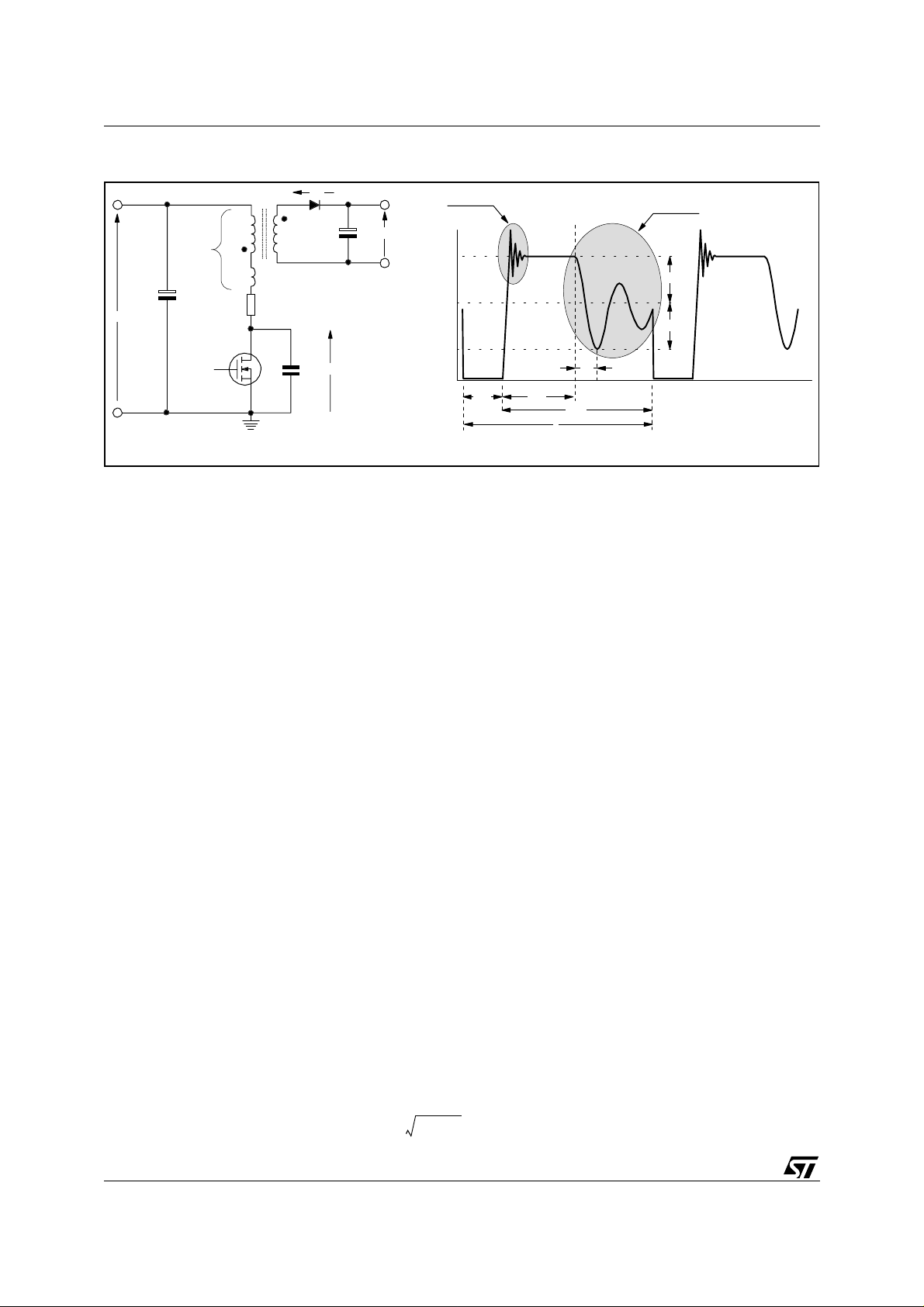
pointing out its major parasitic elements, as illustrated in figure 1.
L
is the leakage inductanc e, which represents the magnetic flux gener ated by the primary winding and no t cou-
lk
pled to the secondary. It stores energy that will not be delivered to the secondary and that needs to be transferred or dissipated elsewhere. Besides, it prevents a portion of the energy stored in the mutual inductance L
(which is perfectly coupled to the secondary) from being transferred to the secondary and delays the energy
transfer process. The energy s tored in L
turn-off.
is the cause of the large overvoltag e spike on the MOSFET's drain at
lk
m
November 2002
1/34
Page 2
AN1326 APPLICATION NOTE
Figure 1.
Vin
Cd is the total capacitance of the drain node. It is the sum of the MOSFET's C
Flyback power stage with major parasitics (a) and VDS waveform with fixed frequency, DCM (b).
Cin
Vf
Lm
Lp
L
Rp
Ls
lk
Cd
V
Vout
DS
a)
V
V
DSs
V
V
DSmin
DS
L
in
lk & Cd
T
d
t = 0
Tv
T
ON
FW
T
OFF
T
Lp & C
V
R
V
R
t
b)
, transformer intrawinding ca-
oss
pacitance, stray capacitance due to the layout of the circuit (e.g. a heatsink) as well as other contributions reflected from the secondary side, such as an R-C damper on the rectifier diode.
Actually, C
and the impact is however limited. Therefore, it is possible to assume for C
= 25V by manufacturers.
V
DS
is discharged inside the MOSFET as it is turned on, thus causing a current spike. This spike not only gives
C
d
is modulated by the drain voltage but the variation becomes significant at very low VDS values
oss
the value specified usually at
oss
origin to additional losses in the MOSFET but may also cause noise problems, especially in case of current
mode control and under light load conditions.
R
is the resistance of the primary side mesh, mostly located in the primary winding. It is important to notice that
p
the resistance of the primary winding has to account not only for the ohmic resistance of the wire but also for
the high frequency effec ts in copper ( skin and proximity), the magnet ic materi al losses (hysteresis and eddy currents) and radiation.
At least a couple of tank circuits can be then identified in the schematic, whose effect is conspicuous on the
drain voltage waveform in Discontinuous Conduction Mode (DCM) operation (see figure 1b).
The first one shows up after the overvoltage spike at MOSFET turn-off and is due to the resonance of L
demagnetized, with C
. The drain voltage falls in under dumped fashion from the peak to the settling value:
d
, just
lk
where V
= Vin + VR = Vin + n · (V
V
DSs
is the DC input voltage, VR the so-called reflected voltage , n the pr imary-to- secondar y turn r atio, V
in
+ Vf)(1)
out
out
the regulated output voltage of the converter and Vf the forward drop across the secondary rectifier.
The second tank circuit, made up of L
and Cd, resonates as the secondary winding has run dry of energy,
p
thus the secondary rectifier no longer conducts, and both windings are open. In principle, it is an RLC circuit
and the drain voltage follows the natural evolution of such circuit starting from the condition of C
@ t = 0 (see waveform in figure 1b). Rp is normally by far less than the critical damping impedance of the
V
DSs
charged at
d
tank circuit, thus the equation describing the under-damped evolution of the drain voltage is:
(t) ≈ Vin + VR · e
V
DS
-α·t
· cos(2 · π · fr · t)
where:
R
p
------------- -=
2/34
α
-------------------------------------=
f
r
π
2
,(2)
⋅
2L
p
1
L
⋅⋅⋅
pCd
(3)
Page 3
are the decay factor and the resonance frequency, respectively.
)
)
The first valley of the resonance occurs at t = T
⋅⋅⋅()
cos 1–T
π
2
frT
v
, where Tv can be derived from:
v
1
v
---------- - π
⋅
2f
r
⇒
L
pCd
AN1326 APPLICATION NOTE
⋅⋅===
;(4)
At that point, the drain voltage experiences an absol ute minim um, given by V
imation ( e
-α·Tv
≈ 1). Therefore, a zero-voltage condition can be generated provided that:
≤ 0 ⇒ VR ≥ V
V
DSmin
in
≈ Vin - VR with good approx-
DSmin
(5)
and, if the system is controlled so that the MOSFET is switched on as the drain voltage reaches either zero or
the minimum of the first valley, a QR ZVS converter will be obtained. The resulting waveforms are shown in
figure 2.
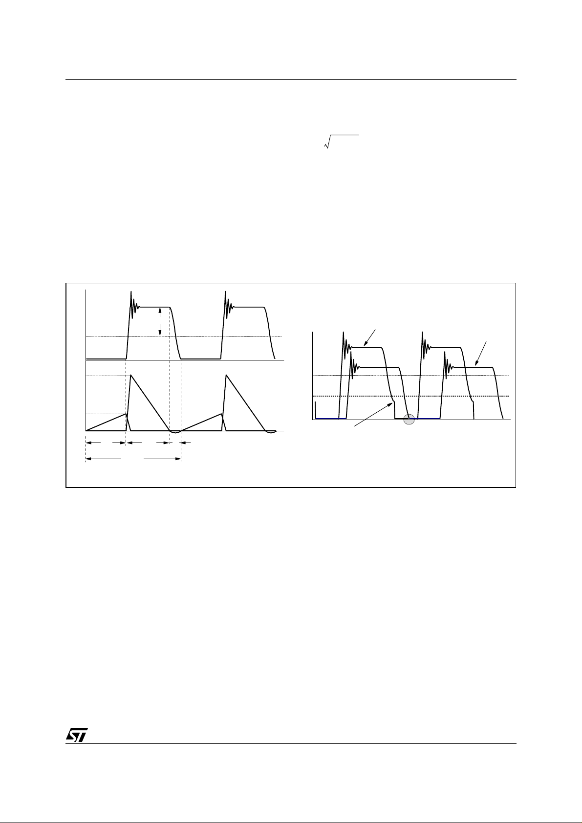
Figure 2. (a) Typical QR waveforms; (b) How Vin affects ZVS conditions.
DS
V
R
in
V
I
PKs
I
I
PKp
Pri Sec
T
ON
T
sw
T
= 1/ f
FW
V
DS
V
t
in2
V
in1
V
NO ZVS! ZVS
v
T
V
DS
@ Vin=V
in2
VDS@ Vin=V
in1
t
a
b
It is worthwhile noticing that the operation of the tank circuit depends only on circuit parameters and not on the
operating conditions of the c onverter . The input v oltage jus t impacts on the zero- vol tage conditi on, as state d by
eqn. 5 and shown in figure 2b.
The key point to generate such kind of functionality is to synchronize MOSFET's turn-on to the transformer demagnetization after an appropriate delay (T
(t). Therefore, in princ iple, any PWM con trol ler with synchr oni zation c apability can be us ed to control thi s
of V
DS
), which can be done just by detecting the negative-going portion
v
kind of converter. The L6565, in partic ular, is provided with a dedicated pin (ZCD) that allows doing the job with
a very simple interface, just one resistor.
Variable frequency operation - as a result of input voltage and/or output current changes - is inherent in such
functionality. The sys tem works clos e to the boundar y between D CM and CCM (Continuous Conduct ion Mode)
operation of the transfor mer. This is what i s otherwise c alled TM ( Transition Mode) operation. The shor ter T
is,
v
compared with the ON and OFF times of the MOSFET, the closer to TM the operation will be. Hence this QR
ZVS flyback converter can be identif ied with the TM flyback converter mentioned in [1], as well as with the wellknown self-oscillating flyback or Ringing Choke Converter (RCC).
As opposed to fixed-frequency standard flyback converter, this approach to quasi-resonance has several advantages.
The main benefit probably c oncerns conducted EMI emi ssions. In mains operated applications , due to the ri pple
appearing across the input bulk capacitor, the switching frequency is modulated at twice the mains frequency
f
, with a depth depending on the ripple amplitude. This causes the spectrum to be spread over frequency
L
3/34
Page 4
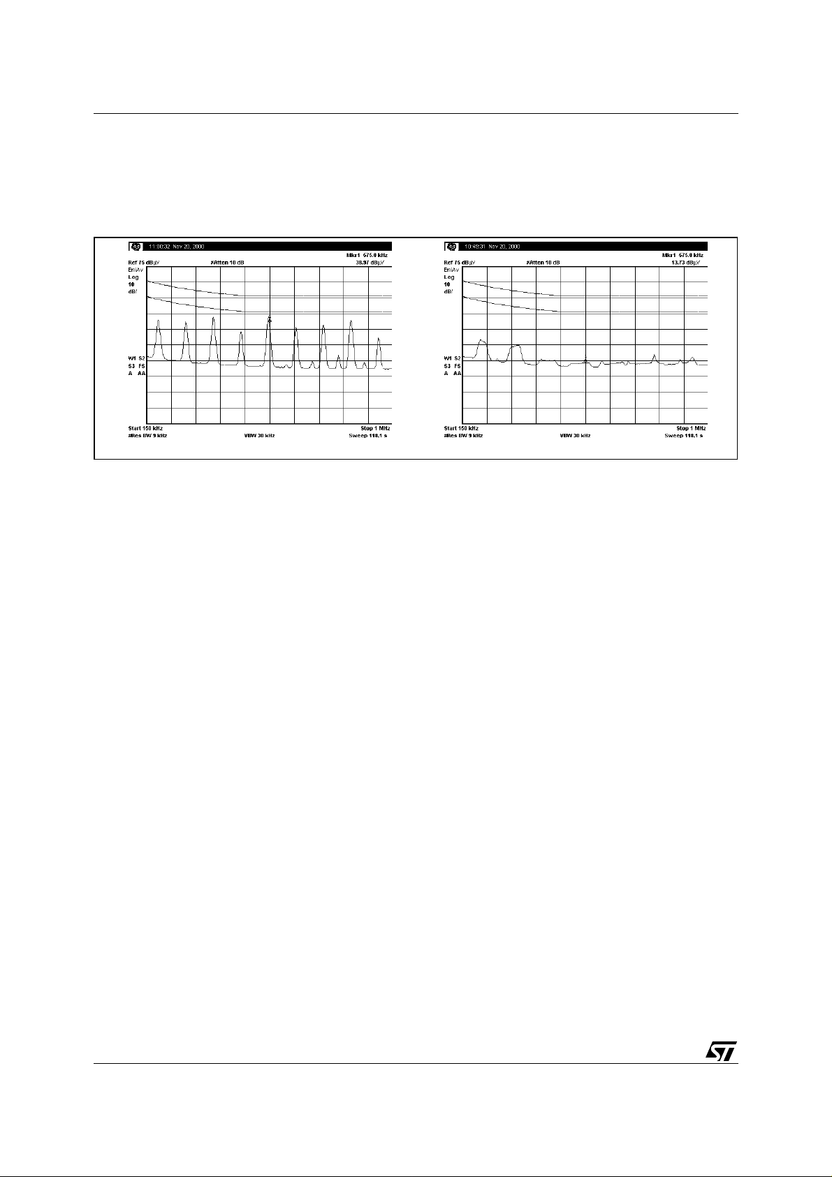
AN1326 APPLICATION NOTE
)b)
bands, rather than bei ng concentrated on singl e frequency values. Especiall y when measuring conducted e missions with the average detection method, the level reduction can be of several dBµV. Figure 3 shows a comparison made on the same L6565-based SMPS, fixed frequency first and then QR-operated. It is then possible to
reduce the size and the cost of the EMI filter.
Figure 3. Conducted EMI (average detection): a) fixed-frequency operation; b) QR operation.
a
Another important benefit is a high safety degree under short circuit conditions: since the conduction cycles of
the MOSFET are inhibited until the transformer is fully demagnetized, flux runaway and, therefore, transformer
saturation are not poss ible. Mor eover, as during a shor t circuit the dem agnetizatio n voltage is very low, the s ystem will be led to work at a very low frequency, with a very s mall duty c ycle. As a result, the power that the converter will be able to carry is very low.
Additionally, QR approach makes use of the otherwise undesirable parasitic drain capacitance to generate a
zero-voltage condition that minimizes turn-on losses of the MOSFET. An external capacitor may be added in
parallel to the MOSFET or across the primary winding. This will reduce the impact that the spread of the parasitic
C
has on fr, smooth the negative-going edge of the drain voltage after transformer's demagnetization (in the
d
interests of EMI) and reduce the dV/dt at turn-off, with the benefit of lower turn-off losses and EMI generation.
Finally, the way the system processes power does not change, thus designer's experience with standard flyback
can be fully exploited and there is very little additional know-how needed.
To complete the pictur e, it must be sai d that t here are al so some draw backs. The sy stem ac tually work s in DCM,
thus currents' peak and RMS values are quite high: this will result mainly in higher conduction losses in the
MOSFET and greater high frequency loss es in the transformer. Thi s suggests not using this appr oach for power
levels above 120-150W in wide range mains applicati ons and above 200 W with European mains. Furthermore,
the high operating frequency when the converter is lightly loaded partly cancels the advantages of the ZVS in
terms of power losses. Finally, while in a standard flyback the design can be optimized in order for a 600V-rated
MOSFET to be used in European or wide range mains applications, optimizing the design in a QR system will
likely lead to the use of a more expensive 800 V-rated MOSFET.
In the following, the topology's operation wil l be d iscus sed in details and a set of equations useful for the des ign
will be given. Then the use of the L6565, a PWM controller specific for this particular topology, will be discussed
in details. Finally, an application (an SMPS for TV) will be developed and the evaluation result of its prototype,
as well as some significant waveforms, will be presented.
QR OPERATION: TIMING AND ENERGETIC RELATIONSHIPS
To generate the equations governing the operation of a QR ZVS flyback converter, with the aim of providing a
design method, some simplifying assumptions will be made:
1) Fall and rise times of both voltage and current waveforms are negligible.
2) Transformer's non-idealities will be neglected (no delay in the primary-to-secondary energy transfer,
peak secondary cu rrent proportional to the primary one dep ending on primary- to-secondary tu rn ra tio n).
3) The system is controlled so that the time elapsed from transformer's demagnetization to MOSFET's
turn-on is kept equal to T
4/34
, eqn. (4), under all operating conditions.
v
Page 5
AN1326 APPLICATION NOTE
That being stated, it will be useful to refer to the simplified schematic of figure 4 as well as the waveforms of
figure 2. The ON-time of the MOSFET is expressed by:
⋅
LpI
PKp
ON
----------------------=
V
in
T
(6)
After T
has elapsed the MOSFET is turned off and energy is transferred to the secondary winding. The time
ON
needed for the discharge of this energy to the output, referred to as "freewheeling time", will be:
L
p
where L
⋅
LsI
PKs
FW
----------------------+
V
outVf
T
is the inductance of the secondary winding and I
s
----- -
n
---------------------------------- -
⋅()⋅
nI
2
+
V
outVf
PKp
⋅
L
pIPKp
----------------------== =
the peak secondary current.
PKs
,(7)
V
R
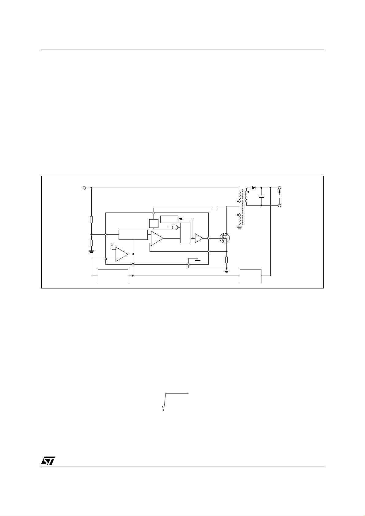
Figure 4. Block diagram of an L6565-based QR ZVS flyback converter.
+Vin
Vout
3
VFF
2.5V
+
INV
1
-
E/A
COMPENSATION
NETWORK
LINE VOLTAGE
FEEDFORW AR D
E/A
2
COMP
ZCD
ZCD
+
-
COMPARATOR
5
PWM
STARTER
L6565
starter STOP
S
RQ
reset
dominant
6
GND
DRIVER
Lp
Ls
GD
7
CS
4
Rs
ISOLATED
FEEDBACK
The total conversion cycle period TSW is the sum of TON, TFW and Tv, and the switching frequency is:
f
SW
1
----------- -
T
SW
-------------------------------------------- -==
T
1
++
ONTOFFTv
.(8)
Since the system actuall y works in DCM, the peak pr imary c urrent is related to the input power of the conver ter,
(more precisely, to transformer's input power), according to the well-known relationship:
P
in
P
in
1
---
2
⋅⋅ ⋅=
L
pIPKp
2
.(9)
f
SW
By substituting (4), (6) and (7) in (8) and combining with (9), the switching frequency can be expressed as a
function of the characteristic parameters of the circuit (L
, VR, fr) and of the operating conditions (Pin, Vin). The
p
result can be conveniently expressed in the following terms:
⋅
2f
T
f
----
f
T
r
12
⋅+++
f
----
f
1
1
1
--------
-------+
V
V
in
R
, (10)
T
r
2
(11)
5/34
where:
f
T
f
SW
--------------------------------------------------------------=
⋅⋅⋅
2P
----------------------------------------------- -=
1
inLp
Page 6
AN1326 APPLICATION NOTE
D
'
1
V
R
-------
2P
out
Lpf
sw
⋅⋅⋅⋅
=
I
ACs
I
RMSs
2
I
DCs
2
–=
V
REV
V
out
1
V
in
V
R
--------+
⋅
=
is the "transition frequency", that is the frequency the system would work at if fr
occur if C
Actually, in case f
(10). The two quantities become more and more different as the ratio f
figure 5), that is as the delay T
= 0. The name comes from the fact that this frequency is characteristic of TM operation.
d
<< fr, it is possible to estimate fsw by using eqn. (11) instead of the more complex formula
T
becomes a significant portion of the switching period Tsw.
v
/ fr increases (see the right diagram of
T
→ ∞ ⇒
Tv = 0, which would
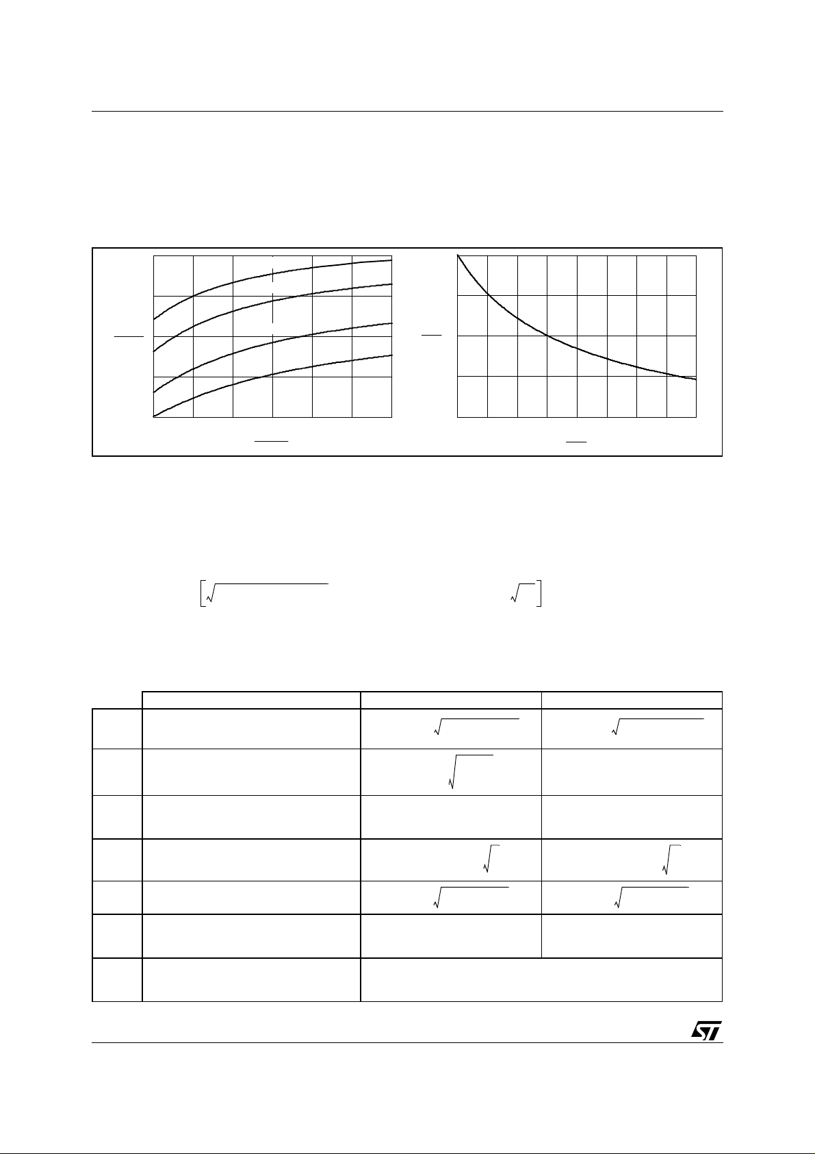
Figure 5. Switching frequency vs. operating conditions (left) and fsw vs. fT (right) relati onships
5
4
sw
f
3
swmin
f
2
1
1 1.5 2 2.5 3 3.5 4
V
0.1·P
0.2·P
0.5·P
in
V
inmin
P
inmax
inmax
inmax
inmax
1.0
0.8
sw
f
0.6
T
f
0.4
0.2
0 0.25 0.5 0.75 1 1.25 1.5 1.75 2
T
f
r
f
The switching frequenc y fsw changes with the operating conditions in so far as the transiti on frequency fT chang-
, f
es, as shown in the l eft diagram of figur e 5. Eqn. ( 11) s hows that the minimum value of f
ally a design constraint, will be reached at maximum input power (P
minimum, V
. Being the converter operated from the AC mains, V
inmin
) when the input voltage Vin is at its
inmax
is the valley voltage across the input
inmin
sw
, which is usu-
swmin
bulk capacitor. Therefore, to fulfill the design requir ement concerning the minimum operating frequency, the pr imary inductance L
L
pmax
will be selected not exceeding the following upper limit:
p
---------------------------------------------------------------------------------------------------------------------------------------------------------=
⋅⋅
2P
in maxfsw min
1
1
----------------- -
V
in min
1
-------+
V
R
⋅⋅+⋅
π
f
sw min
C
2
d
, (12)
The equations that provide the quantities of interest in the design of a QR ZVS flyback converter can be easily
derived considering that the system is inherently of DCM type, although working at a frequency subject to
change with the operating conditions. Table 1 summarizes these relationships.
Table 1. Main Electrical Quantities in QR ZVS Flyback Converters
Parameter Primary Side Secondary Side
1
--------
1 Duty Cycle
2 Peak Current
3 DC Current
4 Total RMS Current
5 AC RMS Current
6 Peak Voltage
7 Switching frequency modulation depth
6/34
D
=
I
I
I
ACp
V
PKDSVinVRVspike
2P
in
PKp
⋅⋅⋅⋅
1
---
=
2
=
2
I
RMSp
2P
------------------=
L
pfsw
I
PKp
V
I
DCp
RMSpIPKp
++=
f
∆
sw
-----------
f
sw
inLpfsw
⋅
in
⋅
D⋅⋅
D
⋅
----
3
2
I
–=
DCp
2f
⋅
-------------------------
=
2f
⋅
2V
–
rfsw
+
rfsw
⋅
----------------------
⋅⋅
V
+
RVin
PKs
I
DCs
∆
-----------
V
V
=
in
in
2I
-------------------=
I
I
RMSsIPKs
R
⋅
DCs
D
'
P
out
-----------=
V
out
D
'
⋅
-----
3
Page 7
AN1326 APPLICATION NOTE
Once the switching frequency has been found from (10), or simply from (11) if that is the case, all of the quantities listed in the table c an be easi ly ca lculated. Obvious ly, c urrent stresses wil l be cal culated at minimum input
voltage and maximum load, while voltage stresses will be calculated at maximum input voltage.
is the power delivered to the load, while the input power Pin that appears explicitly or not in all of the rela-
P
out
tionships should be the one processed by the primary side of the transformer. This is the sum of the power coming out of the secondary side, that lost inside the transformer due to copper and ferrite losses and the one not
transferred (and mostly dissipated in a clamping circuit) because of the leakage inductance. A transformer effi-
η
ciency
could be estimated, such that:
t
P
in
⋅
P
-------------------------------------------=
1
out
η
t
V
f
-----------+
V
out
(13)
The efficiency
technique. If at design-time the designer feels more confident of estimating conv erter's overall efficiency
than transformer's
η
is usually quite high, typically 92 to 98%, depending on transformer's size and construction
t
η
, Pin can be considered as the input power of the converter, that is the ratio of P
t
η
rather
out
to η,
with acceptable approximation.
QR OPERATION: CONVERTER'S POWER CAPAB ILITY AND L6565'S LINE FEEDFORW AR D FUNCTION
Current-mode control wil l be used, thus the maximum power that the sy stem is able to deliver to the output (P
inlim
),
that is its power capability, is controlled by means of pulse-by-pulse current limitation. This is usually done by
clamping the control voltage that programs the peak primary current I
the maximum peak primary current I
PKpmax
.
at a fix ed value V
PKp
, in this way limiting
csx
In fixed-frequency DCM flyback converters, this provides a power capability that, ideally, is independent of the
input voltage V
. Actually, there is a slight dependence due to the internal propagation delay of the controller
in
and the MOSFET's turn-off delay (200 to 500 ns overall).
Differently, in QR ZVS flyback even in the ideal case of no delay , power capability strongly depends on the input
voltage. In wide-range mains applications this can be an issue.
The situation is illustrated in figure 6a. The upper trace shows the primary current waveform at minimum input
voltage: the peak current is close to the maximum, thus just a small extra output power will trip the current limitation circuit. The lower trace shows the primary curr ent waveform under the same load conditions at maximum
input voltage. Being the switching frequency higher, then the peak current will be lower: a much larger power
will be allowed to pass before pulse-by-pulse limitation is tripped.
Figure 6. a) Primary current at min. and max. input voltage; b) Power capability vs. input voltage
I
@Vin=V
p
min
in
I
PKp
max
2.2
2
T
delay
= 400 ns
1.8
in
t
p
I
@Vin=V
in
max
PKp
I
max
t
a)
The effect of such delay is shown in figure 6b, where P
typical design (V
Even ideally (T
= 100 to 400V; P
in
= 0), at 400V input the power throughput that trips the pulse-by-pulse current limitation is
delay
= 125W, f
inlim
swmin
inlim
= 100 kHz, Lp = 110µH, VR = 150V, Cd = 1.5nF).
inmin
@ V
1.6
@ V
inlim
P
inlim
1.4
P
1.2
1
1 1.5 2 2.5 3 3.5 4
in
V
inmin
V
b)
T
delay
vs. Vin is shown for both zero and 400 ns delay in a
about 1.65 times higher than what needed at 100V. Accounting for the delay the limit rises at 2.11 times.
= 0
7/34
Page 8
AN1326 APPLICATION NOTE
To overcome this problem, the L6565 has the Line Feedforward function available. It acts on the clamp level of
the control voltage V
sensed through a dedicated pin (#3, VFF): the higher the input voltage, the lower the setpoint. The diagram of
figure 7a shows the relationship between the voltage at the pin VFF and V
high in the attempt of keeping output voltage regulation). The schematic in figure 7b shows how the function is
included in the control loop.
Figure 7. a) Ove rcurrent se tpoi nt vs . VF F vol t age ; b) Li ne Feedforw ard function blo c k
V
[V]
csx
1.5
, that is on the overcurrent setpoint, so that it is a functi on of the conv erter's input v oltage,
csx
(with the error amplifier saturated
csx
+Vin
V
COMP
= Upper clamp
R1
1
0.5
0
0 0.5 1 1.5 2 2.5 3 3.5
V
[V]
VFF
Quantitatively, the maximum power capability P
PKp
= I
which I
Ideally, the maximum peak primary current I
in table 1 @ V
, substituted in (9):
PKpmax
P
in lim
in
= V
) would be equal to V
inmin
1
---
2
------------------------------------------------------------------------------ -
⋅⋅=
L
p
I
PKp maxLp
PKpmax
/Rs, however the internal pr opagation delay as well as the MOS-
csx
INV
1
2.5V
can be expressed by means of eqns. (6), (7) and (8), in
inlim
2
I
PKp max
(which should slightly exceed the value derived from line 2
R2
COMP VFF CS
23
E/A
+
1
1
--------
-------+
+⋅⋅
T
V
V
in
R
VOLTAGE
FORWARD
v
FET's turn-off delay, has to be accounted for . This causes the actual I
ZCD
5
4
ZCD
FEED
+
PWM
-
+
Hiccup
-
2 V
. (14)
to exceed the ideal value by an
PKpmax
STARTER
Rs
starter STOP
S
R
(reset-dominant)
DISABLE
DRIVER
7
GD
Q
L6565
amount proportional to the input voltage:
I
PKp max
V
------------
csx
Rs
V
--------
L
in
⋅+=
T
p
. (15)
delay
The Line Feedforward bloc k c ombines the v oltage at pin VFF (proportional to the converter's input voltage) with
the E/A output, thus determining th e internal reference (V
) for the PWM comparator, accor ding to the following
cs
relationship:
= 0.16 · (V
V
cs
Note that in this equation V
= 0, which forces the L6565 to stop switching. Actually eqn. (16) is not very accurate when either V
is V
cs
or V
the real V
of V
get close to their respective limits: the effect of offsets and some non-linearity becomes sig nificant. Thus
VFF
= 0 condition and the switching halting may occur for values of V
cs
slightly above 3V
VFF
The overcurrent setpoint (V
is ≥ 2.5V and V
COMP
), graphically illustrated in the diagram of figure 7a, can be found considering the
csx
error amplifier at the limit of its linear dynamics (V
- 2.5) · (3 - V
COMP
) (16)
VFF
is ≤ 3V. Ideally, if either V
VFF
≅ 5.4V). The resulting analytical V
COMP
= 2.5 or V
COMP
slightly below 2.5V and values
COMP
csx
VFF
vs. V
= 3 the result
VFF
COMP
relation-
ship is:
V
= 0.467 · (3 - V
csx
) = 0.467· (3 - k · Vin), (17)
VFF
where k is the divider ratio R2/(R1+R2).
If this function is not needed for any reason, e.g. because of a narrow input volta ge range, the pin w ill be grounded. The overcurrent setpoint will be set at V
8/34
= 1.4V regardless of the converter's input voltage.
csx
Page 9

Figure 8. Correction characteristics of Line Feedforward
2.5
AN1326 APPLICATION NOTE
2
in
inmin
@ V
1.5
@ V
inlim
inlim
P
P
1
in
V
inmin
-3
k=5.07387·10
0.5
1 1.5 2 2.5 3 3.5 4
optimum value
V
The diagram of figure 6b, as well as equations 14 and 15, shows a non-linear relationship between P
and V
, hence the linear correction (17) will not result in a perfect compensation. A considerable reduction of
csx
k=0
k=3.0·10
k=4.0·10
k=6.0·10
-3
-3
-3
, V
inlim
the power capability change over the input voltage range will be achieved anyway.
Figure 8 shows the effect of the compensation circuit on the converter's power capability for different values of
k (a T
The optimum value of k, k
be found by combining equations 14, 15 and 17, imposing that the value of P
of 400 ns is assumed) in the typical design previously considered.
delay
, which minimizes the pow er capability variation over the input voltage range, c ould
opt
is the same at the extremes
inlim
of the input voltage range and sol ving for k. However, the val ue of the sens e r esisto r Rs, which app ears in (15) ,
is a function of k
in turn. The exact calculation is very complex, and non-idealities shift the actual optimum
opt
value from the theoretical one. It is therefore more practical to provide a first cut value, simple to be calculated.
Then, Rs will be chosen on this basis and k
A great simplification comes from assuming T
k
3
opt
⋅=
found empirically.
opt
= 0 (exact TM operation) and T
v
V
-----------------------------------------------------------------------------------------------------------
V
in minVin maxVin minVin max
R
+()V
⋅+⋅
= 0; k
delay
R
will then be:
opt
(18)
in
With k = k
exceeds P
input voltage range and delay, this result does not depend on the specific design, only k
The value of Rs, can be determined from (15), again with T
The approximate calculation yields a value of kopt equal to 3.913·10
5.074·10
After choosing Rs, the value of k
, the maximum value of P
opt
V
@ Vin = V
inlim
-3
.
It can be a useful rule of thum b to use the v alue resul ting from (18) increased by 20% as the st arting point .
inmin
(= P
inlim
opt
, reached at:
inlim
V
in
inx
@ Vin = V
=
s0.467
⋅
VRV
) by about 20%. It is worthwhile pointing out that, for gi ven
inma x
–
3k
-----------------------------------------
⋅
I
----------+
R
k
delay
⋅
V
opt
PKpmax
3
–==
, (19)
V
opt
R
changes.
opt
= 0, resulting in:
inmin
. (20)
-3
, about 23% less than the exact value
can be fine-tuned experimentally to minimize converter's power capability
changes over the input voltage range. To do so, it is necessary to check the power level where the converter
loses regulation just at minimum and maximum input voltage and adjust k (e.g. using a trimmer) so as to make
them equal. This could require, in turn, a modification of Rs, because the power level achieved in the previous
step is slightly higher or lower than the target, thus some iteration might be needed. The values of R1 and R2
will be high enough to minimize the power dissipated on them, especially if there are requirements on the converter's efficiency under light load or no-load conditions.
The small-signal control-to-output-gain of the Line Feedforward block, needed for stability analysis, can be determined by differentiation of the large-signal model (16) and considering that V
ˆ
v
cs
------------------
==
G
FF
ˆ
v
COMP
0.16 3 k
–
⋅()⋅
V
opt
in
VFF
= k
opt
·Vin:
(21a)
9/34
Page 10
AN1326 APPLICATION NOTE
)
)
y
g
Line Feedforward improves also the input ripple r ejection abi lity of the system and limits the variation of the gainbandwidth product of the smal l-signal contr ol-to-output tr ansfer function with the input voltage (see APPENDIX).
The small-signal line-to-output gain of the block is found again by differentiation of (16):
ˆ
v
-------ˆ
v
cs
in
0.16k
optVCOMP
–()–
2.5
'
G
FF
QR OPERATION: BEHAVIOR UNDER SHORT CIRCUIT CONDITIONS
As previously said, a QR flybac k conv erte r operates safely under shor t circui t conditio ns at the output. The r eason of that is that any new conduc tion of the MOSFET is i nhibited as long as the tr ans former is n ot fully demagnetized. Equation 7, which is here recalled:
T
FW
⋅
LPI
PKp
---------------------- -
V
R
⋅
L
PIPKp
----------------------------------- -==
nV
outVf
shows that, as the overload is progressively increased, the demagnetization time T
is kept constant by the pulse-by-pulse limitation and the output voltage drops becaus e the system is out of
I
PKp
regulation. However, if T
before the demagnetization is complete. In some cases, before T
exceeds the period T
FW
of the internal starter, the MOSFET will be switched on
START
FW
so low that the oscillation on the ZCD pin can no longer arm the internal circuit.
Whichever condition is met first, the converter will be forced to work at the frequency of the internal starter (1/
T
) and, likely, in CCM. Flux runaway, though now theoretically possible, is however extremely unlikely.
START
Referring to [2] for the details of the calculations, the flux runaway condition for a dead short at the output is:
⋅
nV
------------------- -
V
inVf
T
f
ONmin
-------------------- -
+
T
START
–
≅≤
10
which is very tough to meet in normal offline applications, as one can easily see by using sensible values for n,
V
and Vf. T
in
is the minimum ON-Time that the L6565 can provi de because of its inter nal delays and MOS-
ONmin
FETS’s Turn-Off delay, usually around 300-400ns.
To guarantee the operation described so far, the L6565 blanks the ZCD input for some time (3.5 µs min.) after
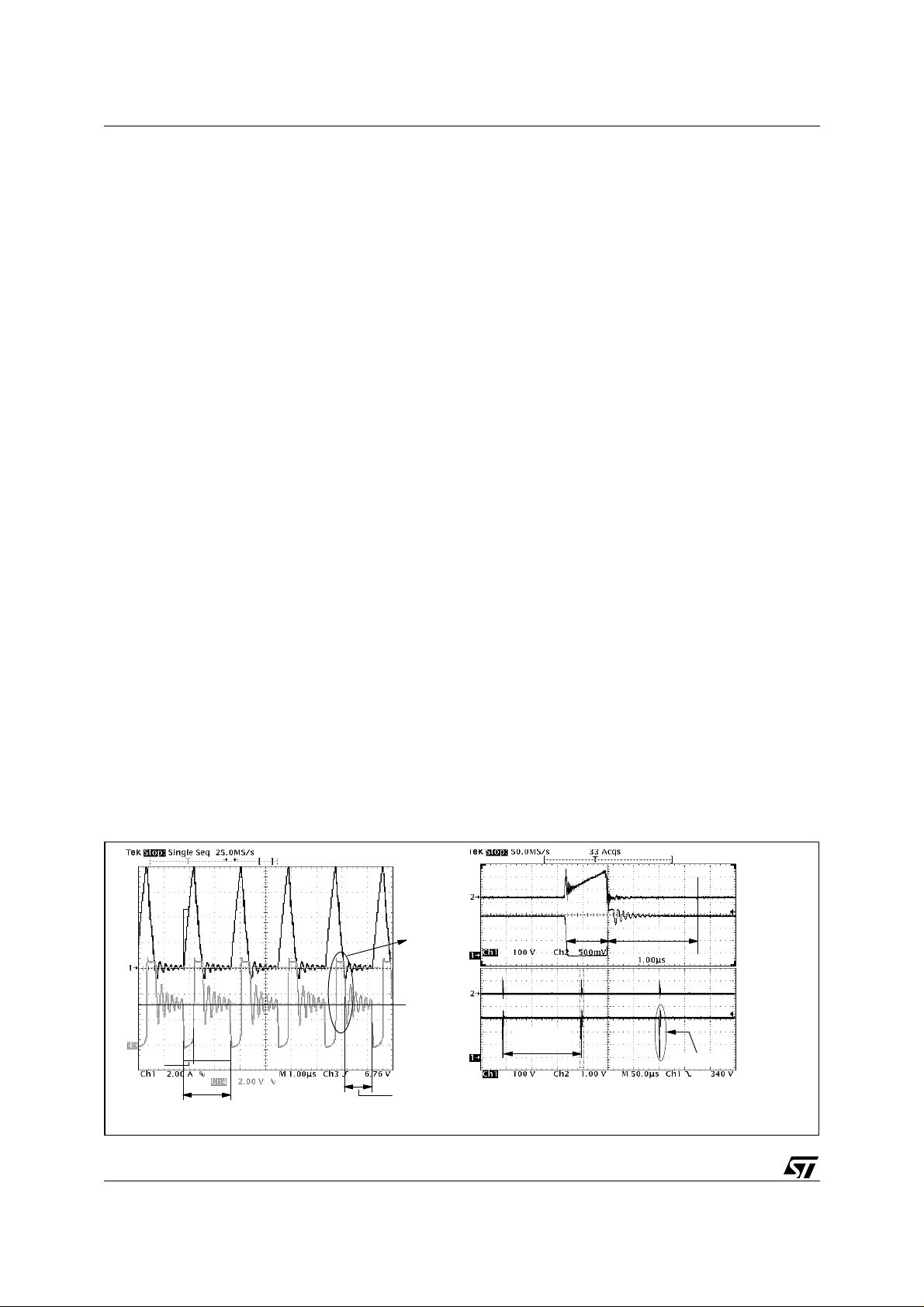
the MOSFET has been turned off. In this way, situations like the one shown in figure 9a, relevant to a short circuit
in a 50W converter using a controller not provided with this safety feature, are prevented. In that picture it is
possible to see that the system is detecting the demagnetization of the leakage inductance and not that of the
primary inductance. This causes a very high frequency operation - instead of a very low one - that has led to
transformer saturation: the primary current reaches a peak of 8A in 400 ns with a slope pointing out only 15 µH
inductance (the overcurrent setpoint was 2A, the primary inductance was 400 µH).
k
opt
-------------------------------- -
–== =
3k
optVin
,
+()⋅
> T
START
3
,
V
.
cs
⋅–
gets longer and longer:
FW
(21b)
, the reflected voltage VR can be
Figure 9. Short circuit waveforms in a system a) without ZCD blanking; b) with ZCD blanking
Primary current
(zoomed)
Drain voltage
(zoomed)
Primary current
Vin = 300 V
Drain voltage
10/34
T
ONmin
LLK ≅15 µH
ON OFF
fsw ≅550 kHz
Primary current
b
T
BLANK
Duty cycle ≈1%
ON
Leakage
inductance
netization
dema
Drain voltage
Vin = 300 V
Internal starter
perio d
ZCD circuit dela
a
T
Page 11
AN1326 APPLICATION NOTE
Figure 9b shows instead the operation previously described, allowed by the L6565, where the converter works
at the frequency of the internal starter with a duty cycle of about 1%.
Dangerous short circuit conditions occur when there is an isolation failure on the secondary winding, e.g. due
to a damaged wire coating, or when the secondary diode fails short (typical of axial diodes). Both of these failures reflect a shor t c ircuit to the transfo rmer' s prim ary sid e while the MOSFET is turned on [2]. The prim ary cur rent rate of rise is then limi ted only by the leakage inductance of the transformer, like in figure 9a. If not properly
handled, this very likely leads to the destruction of the system.
To protect the converter in the event of such failure, a comparator (shown in fig. 7b) senses the voltage on the
current sense input and disables the gate driver if this voltage exceeds the 2
enable the driver, first the IC must be turned off and then restarted: in other words, the Vcc voltage must fall
below the UVLO threshold and then exceed again the start-up threshold.
With the gate driver disabled the quiescent current of the IC is unchanged and, since no energy is coming from
the self-supply circuit, the Vcc capacitor will be discharged below the UVLO threshold after some time (see pin
8 in "L6565 pin usage" section). Then the device will initiate a new start-up cycle. This will result in a low -frequency intermittent operation (Hiccup-mode operation), with very low stress on the power circuit.
QR OPERATION: HIGH SWITCHING FREQUENCY AT LIGHT LOAD AND L6565'S FREQUENCY FOLDBACK FUNCTION
Equations (6) and (7) show that TON and TFW can be however short if I
→ ∞
case f
and fsw → 2·fr. Although in the real-world operation the maximum switching frequency would be
T
PKp
significantly lower than this theor etic al l imit, it cou ld be of som e hundred k Hz and c ause a consi derable efficiency drop. This is why the L6565 has been provided with the Frequency Foldback function.
In principle, this function lies in putting a limit to the minimum OFF-time of the switch [3]. The blanking time of
the ZCD circuit, used for safe operation under short circuit conditions and mentioned in the previous section,
serves this purpose as well. Therefore, the QR operation considered so far will be maintained as long as:
nd
level OCP, fixed at 2V. To re-
(i.e. the load) tends to zero, in whi ch
T
where T
BLANKmin
+ TV ≥ T
FW
BLANKmin
is the aforesaid minimum blanking time (3.5 µs) of the Zero Current Detector (ZCD) circuit.
, (22)
The maximum operating frequency will then not exceed:
f
swmax
----------------------------------------------------------------------------------- -=
T
BLANKmin
1
V
R
------- -+
V
in
–
T
⋅⋅
1
V
R
------- -
v
V
in
.
Figure 10. Frequency foldback: ringing cycle skipping as the load is progressively reduced
V
DS
T
T
FW
V
T
BLANKmin
Pin= P
in'
(limit condition)
V
DS
t
T
BLANK
in''
Pin= P
< P
in'
V
DS
t
T
BLANK
in'''
Pin= P
< P
in''
t
If the load current and the input voltage are such that the condition (22) is not fulfilled, the system will enter the
"Frequency Foldback" mode, a sort of "ringing cycle skipping" illustrated schematically in figure 10.
11/34
Page 12

AN1326 APPLICATION NOTE
Figure 11. a) ZCD blanking time vs. error amplifier output voltage; b) qualitative frequen cy trend
BLANK
T
[µs]
20
15
10
5
0
23456
COMP
V
[V]
a)
Tj = 25 °C
Any negative-going edge of the voltage at pin 5 tha t occurs dur ing the blanking time is ignored; the first negativegoing edge after T
has elapsed will trigger the ZCD circuit and determine MOSFET's turn-on.
BLANK
The peculiarity of the Frequency Foldback function, however, is that the duration of T
error amplifier output V
be and this, in turn, leads to a longer T
, as shown in the diagr am of figure 11 a. The low er the loa d is, the lower V
COMP
. Therefore, more and more ringing cycles will be skipped and the
BLANK
operating frequency will gradually decay, as shown qualitatively in the diagram of figure 11b.
While the Frequency Foldback is active, uneven switc hing cycles may be observed, due to the fact that the OFF-
time of the MOSFET is allowed to change with discrete steps (2·T
cycle energy balance may fall between two contiguous steps. One or more longer switching cycles will be then
compensated by one or more shorter ones, and v ice versa. Thi s phenomenon i s absolute ly normal and there is
no appreciable effect on the performance of the converter and its output voltage.
When the load is low enough, so many ringing cycles and will be skipped that their amplitude becomes very
small and they can no longer arm the ZCD circuit (see pin 5 in "L6565 pin usage" section). In that case, after
some time the ZCD circuit is idle, the interna l starter of the IC w ill be ac tivated, resulting in bur st-mode operation:
a series of few switching cycles spaced out by long periods (400
Actually the operation at very light load can be more complex than so far described: another mechanism may
be involved that interacts with the blanking time of the ZCD circuit.
To explain this mechanism it is useful to r ecall eqn. (16), which provides the output of the Line Feedforward
block (i.e. the internal reference for the PWM comparator): it states that, if the v oltage V
the output V
is zero and the L6565 stops switching.
cs
Depending on parameters such as the input voltage, the residual load (i.e. resistors of the output divider, optocoupler bias, dummy load resistors, etc.) and the tr ansformer's primary inductanc e, at very light load it is pos sible to hit the minimum ON-time (T
≈ 400 ns) of the L6565 and, despite the long switch OFF-times imposed
ONmin
by the ZCD blanking, the energy delivered each cycle may exceed the short-term demand from the load. This
excess energy causes the output voltage to increase a little and the control loop to react by lowering V
until Vcs = 0 and switching is stopped, to maintain the long-term energy balance. The output voltage will now
slowly decay and the control loop will react by increasing V
condition is removed, but will actually restart as the first starter pulse comes after re-enabling. Also in this case
the result will be burst-mode operation.
At most, the burst repetition rate can be as high as the starter frequency but, depending on the converter's output capacitance, the residual load and the control loop response, one or even more starter cycles may be
skipped, giving origin to a burst repetition rate submultip le of the starter frequency. This latter behavior is shown
in fig. 12.
As compared to a bur st-mode operation occ urring at th e starter frequenc y, there is us ually no spec ial advantage
in this starter c ycle skipping mode, since the duration of each burst is longer and the av erage number of sw itching cycles per second, which the light-load losses are related to, does not change much.
sw
f
without
frequency foldback
with
frequency foldback
BURST MODE
in
P
b)
is a function of the
BLANK
), while the OFF-time needed for cycle-by-
v
µ
s typ.) where the MOSFET is in OFF state.
is 2.5V (or lower),
COMP
. Switching will be re-enabled as the Vcs = 0
COMP
COMP
will
COMP
12/34
Page 13

Figure 12. Burst-mode at very light load: starter cycle skipping
AN1326 APPLICATION NOTE
2.52 V
2.28 V
~2 ms
5 starter cycles
COMP
V
Drain voltage
QR ZVS FLYBACK: DESIGN CONSIDERATIONS
■
Minimum switching freque ncy sele ction.
be as high as possible. A high f
swmin
With the aim of minimizing transformer's size, f
swmin
, besides increasing losses, reduces the load range where the converter works in QR, that is, frequency foldback and, eventua lly, burst mode will occur at higher load
currents (which, however, might be desirable). Often, the choice is influenced by EMI considerations too.
■
Reflected voltage selection.
In order to extend the input vo ltage range where t he Z VS condition (5) is
met, the reflected voltage should be a s high as possible. T he upper limit to VR is usually determined
by MOSFET's voltage rating. The selection of V
affects also many important parameters and electrical
R
quantities of the converter, as summarized in table 2. The designer should trade off these sometimes
contrasting requirements one against the other to find the optimum solution for their specific application.
should
Table 2. Effect of VR selection on converter's performance
Increasing (⇑) VR results in:
Parameter Change
Transformer's primary inductance ⇑
Minimum required Transformer's Area Product ⇑
Drain Ringing Frequency ⇓
Switching frequency
⇑(*)
Peak and RMS primary current ⇓
Peak and RMS secondary current ⇑
MOSFET's conduction losses ⇓
MOSFET's turn-on losses ⇓
MOSFET's total losses ⇓ (**)
Secondary rectifier(s) losses ⇑
Maximum drain peak voltage ⇑
Maximum secondary rectifier(s) reverse voltage ⇓
(*) For a gi ven f
■
Transformer design.
ductance is found from (12), the primary- to-sec ondary turn r atio from n = V
, the rate o f rise vs. Vin and I
swmin
Once the electrical specification of the transformer has been defined (the primary in-
increases; (**) At high input voltage; at low input voltage VR has little effect.
out
/ (V
R
+ Vf), the peak and RMS
out
currents from table 1, at minimum input voltage), the desig n of the transformer is carried out jus t like for any
fixed-frequency DCM flyback transformer. R efer to [4] for a handy desig n procedure. A lso the considerati ons
about its construction are exactly the same.
13/34
Page 14

AN1326 APPLICATION NOTE
g
L6565 PIN USAGE
Pin 1
(INV). It i s the inver ting i nput of the E/A. This pin can be us ed in case of both primary and secondar y feed-
back technique, as shown in figure 13.
The circuit for primary feedback shown in figure 13 is recommended when the extremely low consumption be-
fore start-up of the L6565 i s to be fully ex ploited. The parts in the shaded r egion can be omi tted and the res istor
divider (R
consumption of R
Figure 13. Use of L6565's error amplifier
and RH) that sets the output voltage be connected directly to the V cc rail. O f course, in this case the
L
and RH will be accounted for when designing the start-up circuit (see pin 8).
L
+Vin
Vcc
2.5V
R
R
COMP
H
INV
L
GND
Primary Feedback
Rstart
-
+
E/A
L6565
to VFF
block
COMP
Vcc
8
L6565
12
INV
R
A
R
B
Secondary Feedback (type 1)
TL431
Vout
In case of the secondary feedback configuration shown in figure 13, the L6565's error amplifier is used as an
op-amp in inverting configuration, with a gain fixed by the ratio R
. The internal reference is not involved in
A/RB
the output voltage setting (this is done at the secondary side by the TL431); it just sets the quiescent point of
the circuit. The resistors will be selected keeping in mind that the current capability of the E/A must not be exceeded and the gain must be large enough to account for the entire E/A's dynamics.
Pin 2
(COMP). E/A output. Usually, this pin is used for the compensation of the voltage control loop and the
relevant network is connected between this pin and INV (#1), as shown i n the schematics of figure 13. Compensation networks from this pin to ground are not effective since the E/A is a voltage mode type (with low output
impedance).
Figure 14. Use of pin COMP to directly modulate the duty cycle in secondary feedback
Vout
V
COMP
5.8V
2.5V
Regulation
e
ran
3 mA
∆
V
COMP
∆
I
COMP
COMP
I
C
14/34
COMP
L6565
1
2
RB
CTR
Vk
COMP
I
COMPINV
Secondary Feedback (type 2)
TL431
F
I
RH
RFCF
RL
= R
COMP
≈15 k
Ω
Page 15

AN1326 APPLICATION NOTE
In a different type of secondary feedback, s hown in fi gure 14, the pin INV is grounded and the E /A of the L6565
(which is therefore unbalanced high) is used as a current source. The characteristic of this current source is
shown in figure 14 too: the voltage V
I
sunk from the pin within the regulation range. In this region, a change of I
COMP
corresponding to a resistance R
COMP
switching. Anyway, it is recommended to take the pin to G ND not directly, but through a 390 to 470
Pin 3
(VFF). Line feedforward input. Typically, a resistor divider connected as shown in figure 7 applies to this
pin a voltage proportional to the converter's input voltage. Its determination is dealt with in the paragraph describing of the Line Feedforward function.
A small capacitor (typically from 1 to 10 nF), connected between pin 3 and ground is usually recommended to
filter out any noise that may be coupled with the pin (which is a high impedance point).
Pin 4
(CS). Inverting input of the PWM comparator . Through this pin, the L6565 r eads the i nstantaneous inductor current, converted to a proportional voltage by the external sense resistor (Rs). As this signal crosses the
threshold set by the output of the Line Feedforward block, the PWM latch is reset and the power MOSF ET is
turned off. The MOSFET stays in OFF-state until the PWM latch is set again either by an appropriate signal on
the ZCD pin (see pin 5 description) or by the internal starter in the absence of that. An internal circuit ensures
that the PWM latch cannot be set until the signal on the pin CS has disappeared.
The current sense pin can be used in a particular arrangement of the feedback loop shown in figure 15. In this
circuit the optocoupler provides output voltage regulation by modulating the current injected into the offset resistor Roff, depending on the information coming from the secondary side, and changing the dynamics allowed
to the signal across the sens e resistor.
Figure 15. Secondary feedback arrangement suggested for synchronized mode operation
is changed (and the duty cycle controlled) by modulating the current
COMP
causes a change of V
COMP
COMP
≈ 15 kΩ. Forcing pin COMP below 2.25V will cause the L6565 to stop
Ω
resistor.
+Vin
Vout
VFF
VOLTAGE
FEED
FORWARD
Vcc
8
-
PWM
+
4
CS
Second ar y Feedback (type 3)
Roff
TL431
Rs
INV
1
2.5V
COMP
23
E/A
+
L6565
The E/A of the L6565 is not used at all for regulation and stays unbalanced high. This feedbac k arrangem ent is
recommended when the device is required to w ork in synchronized mode and not as a QR controller. In fact,
being the E/A output saturated high, the blanking time of the ZCD is fixed at T
BLANKmin
= 3.5 µs, thus allowing
the IC to be synchronized up to frequencies over 250 kHz, regardless of the line/load conditions.
Pin 5
(ZCD). Input to the Zero Current Detector circuit. Transfo rmer demagnetization will be s ensed through the
auxiliary winding that powers the IC: in fact the voltage developed by this windings is an exact replica of the
drain voltage, scaled down by the primary-to-auxiliary winding turn ratio m (see timing diagram (a) in fig. 16a).
The ZCD circuit is negative-going edge triggered: when the voltage on the pin falls below 1.6V it sets the PWM
latch and the MOSFET is turned on. However, to do so, the circuit must be first armed: prior to falling below
1.6V, the voltage on pin 5 must experience a positive-going edge exceeding 2.1V (typically due to MOSFET's
turn-off in QR operation). This function is realized with a comparator with hysteresis and a monostable that is
positive-going edge triggered, as shown in the block diagram of figure 16. The relevant signals are shown in the
timing diagram a) of figure 16. The ZCD circuit is blanked for some tim e after MOSFE T's turn-off, s o that any
negative-going edge occurring before this time has elaps ed is ignored (see "Frequency Fol dback"). This is illustrated in the timing diagram of figure 17.
15/34
Page 16

AN1326 APPLICATION NOTE
g
Figure 16. ZCD pin internal block diagram and operation
INVCOMP
V
AUX
V
V
ZCD
5.2 V
2.1 V
1.6 V
0.65 V
ARM
TRIGGE R
BLANKING
SET TO THE
PWM LATCH
+Vin
Q
t
t
t
t
t
t
t
to line
FFWD
Synch
Vsmax
V
ZCD
5.2 V
2.1 V
1.6 V
0.65 V
ARM
TRIGGER
BLANKING
V
E/A
blankin
START
A
B
GD
DS
-
+
2.5V
the ZCD circuit
R
Q
S
starter STOP
is armed
BLANK
T
PWM
CCM
DCM
DRIVER
intern al delay
7
the ZCD circuit
is triggered
L6565
R
ZCD
DS
0 V
A
B
GD
ZCD
the ZC D circuit
BLANK
T
5
is armed
150µA
1.6V
2.1V
0.2V
0.3V
the ZCD circuit
is triggered
intern al delay
-
+
-
+
5.2V
MONO
STABLE
A B
DISABLE
t
t
t
t
t
t
t
BLANKING
TIME
STARTER
SET TO THE
PWM LATCH
a) QR mode
t
b) Synchronized mode
t
16/34
Page 17

AN1326 APPLICATION NOTE
Figure 17. Frequency Foldback: timing diagram showing ZCD operation at light load
DS
V
ZCD
V
5.2 V
2.1 V
1.6 V
0.65 V
ARM
GD
A
t
t
t
t
t
t
TRIGGER
BLANKING
SET TO THE
PWM LATCH
GD
B
BLANK
T
t
To minimize the external interface with the synchronization source (whether it is the auxiliary winding or an independent clock), the voltage at the pin is both top and bottom limited by a double clamp. The upper clamp is
typically located at 5.2V, while the lower clamp is at one VB E above zero. The interface will then be made by
just one resistor that has to limit the current sourced by and sunk from the pin within the rated capability of the
internal clamps (3 mA min. each) . To select i ts value, one s hould cons ider the worst c ondition that oc curs while
the MOSFET is in ON-state at maximum input voltage. The minimum resistance value will then be:
V
in max
-------------------1+
m
R
ZCDmin
-----------------------------
3
[k
Ω]=
considering the maximum lower clamp level (1V) and the minimum source capability of the pin (3 mA).
The value can be experimentally adjusted to fine tune the ZCD circuit delay so as to make it equal to T
and
v
optimize MOSFET's turn-on. A higher resistanc e provides a longer delay and vice versa. However, val ues over
Ω
100 to 150 k
R
ZCDmin
have little effect on the delay and, on the other hand, sometimes the minimum resistor value
still provides too long a delay.
In case of need, either of the two circuits shown in figure 18 can be used to extend the adjustment range of the
ZCD circuit delay. In the lag circuit C
is usually a few pF capacitor; its value can be increased according to
ZCD
the need. In the lead circuit the diode limits the negative voltage at -1V, worst case. From the above formula,
the minimum standard value for R
Ω
ZCD to ground is over 5k
, otherwise the L6565 could not start-up. At any rate, the current sunk from the pin
is 680Ω. Now R
ZCD1
must be such that the total resistance from the pin
ZCD2
while the MOSFET is in OFF-state must never exceed the rated capability, then also the following condition
must be met:
R
ZCD2
V
R
-------
–
4.7
m
--------------------- -
3
R
ZCD1
[k
Ω]–>
17/34
Page 18

AN1326 APPLICATION NOTE
g
y
y
y
Figure 18. Circ ui ts to ex te nd th e adj ust m ent range of the ZCD circuit dela y
L6565
ZCD1
ZCD5
ZCD
R
R
ZCD5
≥
Ω
680
L6565
ZCD
C
la
lead
ZCD2
R
≥
4.3 k
1N4148
Ω
If the pin is driven by an external signal, the L6565 will be synchronized to (the negativ e-going edges of) that
signal. To work properly, its period must be greater than the ZCD blanking time, its hig h level V
2.1V and its low level V
lower than 1.6V.
smin
greater than
smax
With reference to the timing diagram b) in figure 16, the minimum limiting resistor will be either:
R
ZCDmin
whichever is greater (provided V
V
-------------------------------
smax
–
s max
4.7
Ω]=
[k
3
is greater than 4.7V and V
or
R
ZCDmin
less than 1V).
smin
+
V
s min
-------------------------
3
1
Ω]=
[k
This pin develops a disable function too. The device w ill be shut down if the v oltage at the pin is forced externall y
below 150mV. To do so, the capability (10mA max.) of the lower clamp has to be exceeded. Any small signal
NPN can be used to do the job.
The IC restarts when the external pull-down is removed (provided its Vcc is still above the UVLO), since an internal 150µA pull-up generator, active only while the IC is disabled, lets the voltage go up. The current consumption during shutdown is reduced at about 1.4mA.
Pin 6
(GND). Ground. This pin acts as the current return for both the signal internal circuitry and for the gate
drive current. When layouting the printed circuit board, these two paths should run separately, as shown in the
schematic of figure 19.
The bold traces carry pulsed high current so they should be as short and fat as possible in the PCB. This w ill
keep both resistive and inductive effects to a minimum, in favor of efficiency as well as radiated RFI.
Figure 19. Rec o m m e nd e d gr ound routi ng i n an L6565-based QR ZVS fly back
Vin
Vac
Secondar
Power GND
Signal GND
Secondar
C
Y1
18/34
VFF
Primar
ZCD
3
COMP
VFB
FBCK
Signal GND
Primary Power GND
5
L6565
GND
Vcc
8
7
GD
6
412
CS
One-poi nt GND
Vout
Page 19

AN1326 APPLICATION NOTE
Pin 7
(GD). Gate driver output. It is able to drive an external MOSFET with 400mA source and sink capability.
The driver is made up of a totem pole with a low side NDMOS. Its inherent body diode avoids the use of an
external diode to prevent excessive negative voltages on the pin due to parasitic ringing.
To avoid undesired switch-on of the external MOSFET, because of some leakage current when the supply of
the chip is below the UVLO threshold, an internal pull-down circuit holds the pin low. This circuit guarantees 1
V maximum on the pin (@ I
between the gate and the source of the external MOSFET used for this purpose.
Pin 8
(Vcc). IC's supply pin. This pin will be externally connected to the start-up circuit (usually one resistor,
R
, connected as shown in figures 20a,b and to the self-supply circuit (aux. winding, diode and C
START
Figure 20. Start-up circuit configurations
= 5mA), with Vcc ≥ 4V. This allow s omitting the "bleeder" resistor connected
sink
SUPPLY
).
Vac
GND
L6565
6
a)
8
Vcc
R
START
+Vin
C
SUPPLY
Vac
R
1N4148
C
START
1N4148
GND
L6565
6
Vcc
8
+Vin
Vac
C
1N4148
optional
SUPPLY
R
START
L6565
6
GND
b)
Vcc
8
+Vin
C
SUPPLY
c)
An additional film capacitor (0.1 or 0.22 µF typically), placed as close the IC's pins as possible, can be used for
filtering out the noise due to layout issues.
To start the L6565, the V
and consumes less than 70µA from the pin, 45µA typically. This allows the use of a high value R
hundreds k
Ω
), or a charge pump circuit, which reduces power consumption and optimizes system efficiency at
voltage must exceed the start-up threshold. Below this value the device is inactive
cc
(in the
START
light load, especially in wide range mains applications.
In principle, to make sure that the IC can start up even with the minimum line voltage (V
imum value for R
voltage to reach the start-up threshold of the IC), R
V
cc
. In practice, however, to get an acceptable wake-up time (i.e. the time needed for the
START
needs to be quite lower than this limit.
START
), there is a max-
ACmin
Figure 21 shows the power consumption of the start-up circuits a) and b) at maximum line voltage when the
device is running, and the typical wake-up time, that is the time needed for the Vcc voltage to reach the startup threshold at minimum line voltage, for different values of R
A minimum value for R
disabled by a 2
nd
level OCP intervention (e.g. resulting from a shorted secondary diode). If a resistance lower
(see Fig. 21 - left) is required to allow the IC to restart after the driver has been
START
than this limit is used, at high line the IC might not restart because the current coming from R
IC consumption (1.6mA min.) and keeps the V
voltage above the UVLO threshold. Of course this feature can
cc
be used the other way round, to turn the Hiccup-mode behavior of the 2
(normalized to its maximum value).
START
nd
OCP threshold into a latched one.
START
exceeds the
19/34
Page 20

AN1326 APPLICATION NOTE
)
)
)
)
Figure 21. Typical power consumption and wake-up time for the start-up circuits a) and b)
W
0.6
Circuit (b
STARTmin
R
= 68 k
STARTmax
= 358 kΩ
= 227 k
Ω
R
R
STARTmax
R
START
0.4
ACmax
@ V
0.2
loss
P
CIrcuit (a
STARTmin
R
STARTmax
= 1550 kΩ
R
0
0.1 0.2 0.3 0.4 0.5
Conditions: Istart-up = 70 µA, Iq = 1.6 mA, Vstart-up = 14.5 V, V
Ω
0.6 0.6
s
3
C
= 47 µF
SUPPLY
2
ACmin
@ V
START
R
STARTmax
R
circuit (a
1
wake-up
T
C
= 22 µF
SUPPLY
0
0.1 0.2 0 .3 0.4 0.5
UVLO
= 8.7 V, Vcc = 12 V, VAC = 88 to 264 VRMS
circuit (b
The start-up circuit c) is a small charge pump. It allows faster wake-up times, compared to circuits a) and b),
with very low power dissipation. The wake-up time depends on the value of C
, a high-voltage capacitor
START
that can be a low-quality one sinc e it is oper ated at low frequency and carries very little c urrent. Figur e 22 shows
the typical wake-up time for different values of C
and the consumption vs. the line voltage. For reference,
STAR T
the consumption of circuit b - but with a much longer wake-up time - is shown too.
Figure 22. Ty pi cal po we r co nsu m pt i on and wa ke-up time fo r the sta rt- up ci rc u it of figure 20c
T
P
0.25
0.15
loss
0.2
[W]
C
SUPPLY
= 47 µF
Circuit (b )
Twake-up = 3 s @ 88 V
AC
wake-up
10
8
6
[s]
VAC= 88VRMS
0.1
0.05
0
50 100 150 200 250 300
VAC[VRMS]
Circuit (c)
Twake-up = 1 s @ 88 V
R = 100
Ω
AC
The above-mentioned considerations that lead to a minimum value for R
limit of 85nF to the maximum value of C
(the current delivered by the pump is ·VAC·fL·C
START
series resistor R limits the charge/discharge peak current of C
4
2
C
= 22 µF
SUPPLY
0
20 40 60 80 100
START
C
[nF]
START
in circuits a) and b) here put a
START
. It may range from few units to some k
SUPPLY
C
= 47 µF
2
START
). The
Ω
without affecting the wake-up time significant ly; howev er, the dissipati on will go up as R increases above some
hundred ohms.
When operating, the current consumption (of the device only, not considering the gate drive current) rises to a
value not exceeding 3.5mA. The device keeps on working as long as the supply voltage is over the UVLO
threshold (10.3V max). If the Vcc voltage exceeds 18V (min.) an internal zener diode, 25mA rated, will be activated in order to clamp the voltage. In that case the consumption of the device will obviously increase.
20/34
Page 21

AN1326 APPLICATION NOTE
A PRACTICAL QR ZVS FLYBACK DESIGN WITH THE L6565
As a reference design, a 50 W multioutput QR ZVS flyback converter for a 14" TV SMPS, based on the L6565,
will be now presented.
Table 3 summarizes the electrical specification of the application, table 3 provides transformer's spec, and the
electrical schematic is shown in figure 23 along with the relevant part values.
Table 3. L6565-based 50W QR SMPS for 14" TV: electrical specification
Input Voltage Range (Vin) 88 to 264 Vac
Mains Frequency (f
Maximum Output Power (P
Outputs V
Minimum Switching Frequency in Normal Mode 70 kHz
Target Efficie ncy (@ P
Maximum Input Power in Standby
(@ P
= 0.25 W on 5V output, Vin = 88÷264 Vac)
out
) 50/60 Hz
L
) 51 W
out
= 105 V ± 5%
out1
= 0.1 to 0.35 A
I
out1
V
ripple1
= 14 V ± 10%
V
out2
=0.1 to 1 A
I
out2
V
ripple2
V
= 5 V ± 5%
out3
= 50 mA
I
out3
V
ripple3
= 50 W, Vin = 88÷264 Vac) η > 80%
out
< 2 W
= 1%
= 1%
< 1%
The minimum switching frequency (70 kHz @ Vin = 90VDC) has been chosen trading off transformer's size
against frequency-related losses. The reflec ted voltage is 140V, thus ZVS is achieved only when the converter
is powered by the 110V mains. H owever, this value seems to provide a good compromise between capacitive
and switching losses at 220 V mains. An 800V MOSFET is used anyway to provi de enough room for the l eakage
inductance voltage spike, in order to maximize energy transfer during its demagnetization.
The converter is started up with a dropping resistor (R1+R2) that draws current from the AC side of the bridge
rectifier. This circ uit dissipates only about 240m W @ 264 Vac thanks to the extremely low start-up current of the
L6565. The worst-case wake-up time is 2.8s at 88 Vac and 0.7s at 264 Vac.
R3 and R4 compensate for the power capabil ity c hange vs. the input v oltage (V oltage Feedforw ard). A 1nF fi lm
capacitor bypasses any noise on pin #3 to ground.
Output voltage regulation is achi eved with secondary feedbac k, type 1; Vout1 (105V), which must be tightly regulated, is directly under feedback and Vout2 (14V) is in tracking. The 5V output for the µP is linearly post-regulated from the 14V output to get a very clean voltage.
21/34
Page 22

AN1326 APPLICATION NOTE
Figure 23. L6565-based 50W QR SMPS for 14" TV: electrical schematic
Vin
88 to
264 Vac
1 nF
2A fuse
C3
F1
C23
100nF
R3
3 M
16 K
C6 4700pF/ 4KV
NTC1
16R
C25
1nF
C24
100nF
L1
15mH
IC1
VFF
R4
L6565
3
2
COMP
R12
47 k
C5
2.2 nF
1
B1 2KBP04M
C26
1nF
5
7
4
8
6
GNDINV
R13
3.3 k
D1
1N4148
ZCD
GD
CS
Vcc
C1
150 µF
400 V
C27
220nF
R1
75k
R2
75k
DZ1
15 V
100 k
R20 22 k
R5
R7 10
C8
8.2 nF
250 V
D3 STTA106
R8 22
C4
47µF
25V
R6 100
D2
1N4148
1N4148
R14
1.5 k
C2
180 pF
630V
D4
R11
0.47
STP7NB80FI
R9
4.7M
3
N1
1
4
Naux
5
Q1
IC3 PC817
4
3
IC2 TL431
C7 4700pF/ 4KV
R10
4.7M
T1
8
N2
9
N3
10
1
2
1
2
3
100 pF
BYT01-400
D6
BYW98-100
R15
1.8 k
220 k
C22
R16
D5
C13
100 nF
C10
470 µF
25 V
100 µF 2 5V
220 µF
C12
C9
160 V
P1
100 k
R18
150 k
R17
4.7 k
105 V
0.35 A
14 V
1 A
+5 V
3
50 mA
C11
47 µF
25V
12
IC4
L7805
Table 4. L6565-based 50W QR SMPS for 14" TV: transformer specification
Core ETD29/16/10, N67 Material or 3C85 or equivalent
Bobbin Horizontal mounting, 14 pins
Air gap ≈
1 mm for an inductance 1-3 of 285 µH
Leakage inductance < 8 µH
Windings
Pin Start/End Winding Voltage Wire Turns Notes
Spec & Build
1/2 Pri1 --- 2xAWG28 24
8/9 Sec1 105 AWG28 31
9/10 Sec2 14 AWG28 5
2/3 Pri2 --- 2xAWG28 24
4/5 Aux 14 AWG32 5 Evenly spaced
A protection against output overvoltages (OVP) due to the optocoupler's failure is realized with the zener diode
DZ1. In case of failure the output voltage w ill not be out of control: the system will work with a primary voltage
sensing feedback that regulates the outputs 10-15% higher than the nominal value.
A 180pF polypropylene capacitor has been added across the primar y winding to optimiz e MOSFET' s losses by
a small snubbing effect on the drain voltage rate of rise.
The delay between transformer' s demagnetization and MOSFET's turn-on is adjusted by means of R20. The
22/34
Page 23

AN1326 APPLICATION NOTE
final value of 22kΩ has been experimentally determined so as to achieve the optimum turn-on point after the
addition of C2. Changing the value of C2 requires a different value of R20.
The following tables summarize some signific ant evaluation data of the prototype and the oscil loscope pi ctur es
show some significant waveforms under different operating conditions.
Table 5. L6565-based 50W QR SMPS for 14" TV: Full load measurements
VAC [V]
88 110 132 176 220 264
Pin [W]
61.7 60.4 59.0 58.7 59.7 61.2
105.0 105.0 105.0 105.0 105.1 105.1
Vout [V]
13.74 13.76 13.77 13.77 13.78 13.78
4.995 4.995 4.995 4.995 4.995 4.995
[W]
P
out
[%]
η
50.74 50.76 50.77 50.77 50.78 50.78
82.2 84.0 86.0 86. 5 85.1 83.0
Load conditions: 105V: 350mA; 14V: 1A; 5V: 50mA
Table 6. L6565-based 50W QR SMPS for 14" TV: consumption from the mains in Standby
[V]
V
AC
Pin [W]
88 110 132 176 220 264
1.17 1.20 1.24 1.37 1.45 1.60
Load conditions: 105V and 14V open; 5V: 50mA
Table 7. L6565-based 50W QR SMPS for 14" TV: power capability
V
P
AC
inlim
[V]
[W]
88 110 132 176 220 264
86 92 96 98 95 90
Figure 24. Drain Voltage and Primary Current: Full load, V
Ch2: Q1 drain volt age
Ch3: current s ense pin
= 100 VDC (left), Vin = 380 VDC (right)
in
Ch2: Q1 drain volt age
Ch3: current s ense pin
23/34
Page 24

AN1326 APPLICATION NOTE
Figure 25. Drain Voltage and Primary Current: half load, Vin = 100 VDC (left), Vin = 380 VDC (right)
Ch2: Q1 drain voltage
Ch3: current sense pin
Figure 26. Drain Voltage and Primary Current: Standby, V
Ch1: Q1 drain voltage
Ch2: current sense pin
Figure 27. Sh ort circuit on 105V output, V
= 300 VDC: system running at the starter frequency
in
Ch2: Q1 drain voltage
Ch3: current sense pin
= 100 VDC (left), Vin = 380 VDC (right)
in
Ch1: Q1 drain voltage
Ch2: current sense pin
24/34
Ch1: Vcc (pin 8) voltage
Ch2: Q1 drain voltage
Q1 drain voltage
Lower screen: detail of a burst
Upper screen: detail of a single cycle
Page 25

AN1326 APPLICATION NOTE
Figure 28. Short circuit of the output diode D5: detail of turn-on (left), Hiccup-mode operation (right).
Ch1: Q1 drain voltage
Ch2:current sense pin
Figure 29. Uneven ringing cycle skipping during frequency foldback
Ch1: Q1 drain voltage
Ch2: 105 V output
Figure 30. Details of MOSFET turn-on; V
= 100 VDC (left) - ZVS, Vin = 300 VDC (right) - no ZVS
in
Ch1: Q1 drain voltage
Ch2:current sense pin
Ch3: Q1 drain voltage
Ch4: current sense pin
Ch3: Q1 drain voltage
Ch4: current sense pin
25/34
Page 26

AN1326 APPLICATION NOTE
)
(t)
(t)
)
(t)
(t)
CONCLUSIONS
After showing how it is possible to obtain a QR ZVS flyback converter suitable for offline applications from a
standard fixed-frequency flyback converter, the many benefits and the few drawbacks resulting from this approach have been highlighted.
The equations governing the operation of such class of converters have been derived for design purposes and
some details have been considered, resulting in some clues on their design. Details on how the L6565 and the
functions it embeds are to be used are given. In particular, the Frequency Foldback and the Line Feedforward
functions have been discussed.
A detailed pin-by-pin description of the IC has been provided, with some hints on pin usage. Finally, as an example, a 50W multioutput QR ZVS flyback converter for 14 " TV SMPS, along w ith benc h evaluati on results and
the most significant waveforms, has been presented.
REFERENCES
[1] "L6561-based Flyback Converters" (AN1060)
[2] "How to handle Short Circuit Conditions with ST's Advanced PWM Controllers" (AN1215)
[3] Y. Panov, M. Jovanovic, "Adaptive Off-Time Control For Variable-Frequency, Soft-Switched F lyback Con-
verter At Light Loads", PESC 99. 30th Annual IEEE (1999 Volume 1)
[4] L. H. Dixon, Jr., "Filter Inductor and Flyback Transformer Design for Switching Power Supplies", Unitrode
Switching Regulated Power Supply Design Seminar Manual, SEM-1000, 1994
[5] J. Ch en, R. Eri ckson, D. Maksimo vic, "Aver aged Swit ch Modeling of Boundary Conduction Mode DC-to- DC
Converters", IECON ’01. 27
th
Annual IEEE (2001 Volume 2)
APPENDIX
QR operation: M O S FE T's t ur n- on
As can be noted in the detailed waveforms of figure 31, the primary current becomes negative during the dead
time Tv. It is a portion of sinusoid since it is related to a resonance. This is due to the drain capacitance that is
discharging, thus current comes out of the MOSFET's drain and charges the primary inductor L
.
p
Figure 31. Details of MOSFET's turn-on in case of: (a) Vin > VR, no ZVS, (b) Vin < VR, ZVS
DS
V
in
V
sinusoidal
curre n t
in
R
V
- V
t=0
Tv
in
R
V
+ V
capacitive
curre n t sp ike
p
I
DS
V
in
R
V
+ V
linear
sinusoidal
current
in
V
current
p
I
t=0
F
-V
PKp
I
MOSFET
turn-on
a
T1 T2
Tv
b
MOSFET
turn-on
I
PKp
26/34
Page 27

AN1326 APPLICATION NOTE
(t)
(t)
This being a reactive current, the associated power dissipation inside the MOSFET is ideally zero, negligible in
practice. Some power is dissi pated in the equivalent resistanc e of the primary winding, lik e in a standard flyback
converter operated in DCM.
If the ZVS condition (5) is not satisfied, the residual drain voltage generates a current spike at MOSFET's turnon (see figure 31a) due to the sudden discharge of C
that can be expressed as follows:
5
P
cap
---
C
ossVinVR
6
–()
through MOSFET's R
d
3
-- -
2
1
---
⋅⋅+⋅⋅
C
dVinVR
2
–()
ds(ON)
2
⋅=
f
sw
. There is an associated loss
, (A1)
where C
non-linear nature of C
is the MOSFET's drain-to-source capacitance s pecified at VDS = 25V. The above formula takes the
oss
into account ant assumes that the remaining part of Cd is linear.
oss
When the ZVS condition is met, the loss quantified by equation A1 is zero but a power loss will be generated in
the MOSFET if its body diode is injected. In order for that to happen, it is sufficient that the reflected voltage
exceeds the input voltage by one diode drop (assume typically 1 V).
Figure 31b shows the situation in details. At the time T
MOSFET's body diode. Then the current turns from sinusoidal to linear. It takes a time T
to zero and the power dissipation occurs during this time. To simplify, C
glected with respect to V
. With these approximations, the estimated power loss will be:
in
P
diode
⋅
VFI
DCdiode
the drain voltage reaches -VF and is clamped by the
1
for the current to go
2
1
---
2
V
--------------------- -
⋅⋅ ⋅⋅==
V
F
modulation is ignored and VF is ne-
oss
2
2
–
V
R
in
C
V
in
dfsw
This dissipation usual ly amounts at some ten mW at minimum input voltage, which is the worst case. As a result,
there is no point in complicating the control to turn-on the MOSFET exactly when the drain voltage crosses zero
to avoid body diode injection. A fixed dead-time T
is the optimum solution in most cases.
v
QR operation: MOSFET's turn-off
When the MOSFET is driven off, the drain current star ts to decrease with a certain slope from its peak value
I
. The transformer's primary inductance acts almost as a current source, thus this current decrease is mir-
PKp
rored by a current increas e through C
coupled with L
and the voltage across Lm will be fixed at Vin + VR. The drain voltage will increase further on
s
because the leakage inductance L
tized. When L
has run dry the drain voltage will settle down to Vin + VR after some oscillations.
lk
. The drain voltage will ris e until it reaches Vin + VR, after that Lp becomes
d
is still charged with a current almost equal to I
lk
and has to be demagne-
PKp
Figure 32. Details of MOSFET's turn-off: linear approximation of current falling edge.
DS
p
I
PKp
I
PKp
0.9·I
PKp
0.1·I
T
PKp
I
S0=
F
F
T
2
T
F
2·T
F
T
2
R
V
Vin+ V
R
With the approximation sketched in fi gure 32, the drain voltage ev olution w ill be described by a sinusoi d that, in
27/34
Page 28

AN1326 APPLICATION NOTE
almost all practical cases, can be approximated by a parabola:
I
PKp
--------------------------
()
with a small error. T
VDSt
is the current fall time (defined as the time needed to the current to fall from 90% to 10%
F
⋅⋅
4TFC
of its initial value) that can be deduced from the MOSFET's electrical specification.
The time T
needed to the drain voltage to reach the level Vin + VR, when the leakage inductance begins its
R
demagnetization (practically, the drain voltage rise time), will be:
T
FCd
--------------------------------------------------⋅=
2
T
is such that TR > 2·TF, that is if:
If C
d
R
>
C
d
I
PKp
⋅
TFI
PKp
---------------------- +
V
inVR
then the turn-off losses in the MOSFET will be given by:
2
⋅()
TFI
PKp
sw
------------------------------ -
⋅
6C
d
P
By inspection of (A1) and (A2) it is possible to see that there is an optimum value of C
FET's total switching losses P
+ Psw. With some easy calculation it is possible to find:
cap
T
1
FIPKp
---------------------- -
-------
C
dopt
⋅=
V
3
Usually, an external capacitor should be added to get such capacitance value.
However, this optimization is valid only under specific oper ating conditions, in terms of input voltage and load
current. For example, optimizing losses for full load conditions will inevitably lead to higher losses at light load.
This should be kept in mind when deciding whether to use or not the capacitor.
Another consideration could be that the addi tion of s uch cap acitor coul d allow the d esigner to s ave the RCD (or
zener) clamp for the leakage inductance spike. To be able to do this, the total drain capacitance has to meet the
condition:
2
⋅
I
L
PKp
--------------------------------------------------------------
>
C
d
V
()
BR
DSSVin
lk
–
2
⋅=
t
d
+()⋅⋅
V
inVR
,
⋅=
. (A2)
f
sw
⋅
–
inVR
(A3),
2
–[]
V
R
that minimizes MOS-
d
where V
(BR)DSS
is the breakdown voltage of the MOSFET. This cond ition shoul d be evaluated und er the worstcase conditions that are with the short circuit peak primary current and at the input voltage where the right side
of (A3) reaches the maximum, which generally occurs at V
in
= V
inmax
.
Anyway, if used, it is advantageous to connect the external capacitor across the primary winding of the transformer: in this case its voltage rating needs to be greater than V
V
inmax+VR
if connected across the MOSFET. The effect on fr and the drain voltage rise time will be the same.
, whereas it should be rated at least for
inmax
Small signal model of QR ZVS flyback and design of the feedback loop compensation
The control loop can be summarized as shown in figure 33, where each block is described by its transfer function
in the complex frequency domain and represented by means of a Bode plot. The set PWM modulator + Power
stage + Line Feedforward block is what, in control theory terminology, is called the "plant", while the compensated error amplifier is the "controller".
The task of the control loop design is to determine the transfer function G1(j
ω
) of the error amplifier and define
the relevant frequency compensation network. The objec tive of the design is to ensure that the resulting closed-
28/34
Page 29

AN1326 APPLICATION NOTE
g
loop system will be stable and well performing in terms of regulation and dynamic response.
Figure 33. Control loop Block Diagram of an L6565-based QR ZVS flyback
^
Vin
G2(jω)
Vref
+
-
ERROR AMPLIFIER
G1(jω)
^^ ^ ^
COMP
V
LINE
FEEDFORWARD
G
FF
FEEDBACK
+
CS
V
-
PWM MO DULATOR
G
PWM
Rs
i
PKp
POWER STAGE
G2'(jω)
Vout
H
To do so, it is necessary to determine first the transfer function of the plant G2(jω), in order to select an appropriate structure for G1(j
ω
). The transfer function of the plant is defined by the control method ( peak current
mode), the topology of the converter (flyback) and its operating mode. For the sake of simplicity the operating
mode will be c onsidered an exact TM (transiti on Mode), neglecti ng the time Tv needed to achi eve ZVS. An ex act
analysis considering also the dead time, besides being much heavier from the calculation point of view, would
show that the difference is practically negligible at least at medium-heavy load.
ω
G2(j
) can be factorized as the product of the gain of the Line Feedforward block (GFF), the PWM modulator
gain (G
The expression of G
) and the power stage transfer function G2'(jω):
PWM
ω
) = GFF · G
G2(j
is given in (21a), while that of G
FF
G
PWM
PWM
ˆ
i
PKp
---------- ˆ
v
cs
PWM
· G2’(jω).
is simply:
1
-------==
Rs
As to the power stage , an analys is with the averaged swi tch mo del app roach [5] leads to the small-signal model
illustrated in figure 34.The resulting control-to-output transfer function G2'(j
ω
) is:
Figure 34. Small-signal model of the QR ZVS power stage
∧∧
1
in
= i
i
∧
1
g21·v
∧
1
v
+
∧
in
v
-
∧
PKp
i
2
∧
2·iPKp
j
Averaged switch model
g22·v
∧
2
Lp
∧
i2=
∧
C
2
v
2
n·R
∧
out
i
n
−
D1
=
j
2
2
out
2
2
n
c
n·R
out
n·v
=
∧
out
21
−=
22
1gD
2
Rn
out
D
2
Rn
out
2
−
D1
29/34
Page 30

AN1326 APPLICATION NOTE
L
------------------
–
ω
n2R
R
outCout
-----------------------+
1D
p
out
D
-------------------- -
–()
1D
2
G2'j
ω()
ˆ
v
out
----------ˆ
i
PKp
+()
1jωR
R
out
–
1D
------------------------------------------------------------------------------------------------------ -==
------------- +
1D
n
-- -
2
cCout
1j
+
ω
1j
which looks very much like the low-frequency approximation of the control-to-output transfer function of CCM
flyback:
■
the DC gain o f the control-to-output transfer function is exactly half that of a CCM system;
■
there is a low-frequency shifting pole exactly equal to that of a CCM system;
■
the gain-bandwidth product is a function of the input-to-output voltage ratio only, like in CCM systems.
■
there is a shifting RHP zero with the same expression as in a CCM system, but actually located at a
higher frequency because of the smaller inductance; it is possible to show that:
f
RHP
f
,
sw
π
D
1
------- -
=
which is well above usual targets of the open-loop crossover frequency and therefore will be neglected for
loop design purposes. If the crossover frequency is selected higher than 0.1f
there will be some phase
RHP
margin erosion that can be accounted for at design time.
------
14
n
R
out
----------- -
Rs
ω
) will be:
–()
3k
optVin
1jωR
–
1D
----------------------------------------
------------- +
1D
+
1j
+()
cCout
R
outCout
------------------------
ω
1D
,
+
Finally, the control-to-output transfer function G2(j
ˆ
v
out
==
ω()
G2 j
-----------------ˆ
v
COMP
being 0.14/2 = 0.07
≅
1/14.
It is worthwhile notici ng that the Line Feedfor ward block a ffects the dependence of the control-to-output DC gain
on the input voltage. Moreover, it is possible to prove also that it reduces the variation of the gain-bandwidth
product of G2(j
ω
) versus the input voltage exactly the same way it compensates converter's power capability.
In case of optimum compensation, this means that it assumes the same values at the extremes values of Vin
and reaches a maximum, 20% higher, for V
in
= V
given by (20). This is shown in figure 35 for the converter
inx
example considered in the text.
Although the crossover frequency of G2(j
design purposes it is still better to consider the condition V
ω
) is maximum for Vin = V
in=Vinmin
its increase is relatively small, then for
inx
where the RHP zero frequency is minimum
and its effects are maximum.
Figure 35. Ty pi c al Bode plots of G2 (jω) under different operating conditions
60
V
= V
in
40
Min. / Max. V
Min. load
20
V
in
dB
Min. / Max. Vin, Max. load
0
20
40
1101001
= V
, Max. load
inx
in
ω
)
G2(j
¦G¦ /G
, Min. load
inx
.
1031.1041.1051.10
f
6
0
20
40
deg
60
80
100
0.1 1 10 100 1.1031.1041.1051.10
V
= V
in
Min. load
V
= V
in
Max. load
Min. / Max. V
Min. load
inx
inx
ω
G2(j
Min. / Max. V
Max. load
in
f
)
in
6
30/34
Page 31

AN1326 APPLICATION NOTE
)b)
It is interesting to consider the audio susceptibility as well, that is the line-to-output transfer function, and see
the effect of the Line feedforward block. The line-to-output transfer function of the powe r stage only, that is w ith
the VFF pin grounded or kept at a fixed voltage, is:
ˆ
v
out
---------ˆ
v
=
in
1
D
-- -
----------------
n
–
1D
2
+
1jωR
----------------------------------------
2
+
ω
1j
R
----------------------- -
cCout
outCout
+
1D
.
The gain of the vol tage feedforward block with respect to the input vol tage changes, G'
reference to the small-signal model of figure 34, this means that the current generator is no longer in-
ˆ
dependent (and cannot be opened) but is a function of . The resulting expression is:
+()
1jωR
α
--------------------------------------------------------------------------------------------------------------------- -=
--- -–
D
ˆ
v
out
---------ˆ
v
2
1
D
----------------
-- -
n
in
1D
2
–
1
where:
α
v
in
cCout
k
optVin
----------------------------=
–
3k
optVin
1j
+
1j
------------------
+
ω
n2R
R
outCout
----------------------- -
ω
1D
L
p
+
out
D
-------------------- -
–()
1D
, is given by (21b). With
FF
1
ˆ
-- -
i
PKp
2
α
------------- -
2
α–
D
The Line Feedforward then modifies the DC gain with an additional factor and adds a shifting zero. A simple
inspection shows that the D C gain is positive for
time, the additional zero disappears for
α
prove that
equals D (which nulls the DC gain and the zero location) for Vin = V
α
α
<D, negative for α>D and zero for α=D, and that, at the same
=D, is an LHP ze ro for α<D, an RHP zero for α>D. It is possible to
given by (20).
inx
Figure 36. Open-loop audio susceptibility: a) DC gain; b) 100 Hz gain
=ω
2π100
0.015
without Line Feedforward
0.01
0.005
with Line Feedforward
k=k
opt
0.06
without Line Feedforward
0.04
^
ˆ
v
out
ˆ
v
in
=ω
0
0.02
with Line Feedforward
k=k
opt
v
out
^
v
in
0
1 1.5 2 2.5 3 3.5 4
Vin
a
0
11.522.533.54
Vin
Figure 36 shows how the overall audio susceptibility @DC and @100 Hz change over the input voltage range,
compared against the gain that would result with k=0, that is without Line Feedforward. It is possible to notice
that in the lower input voltage range, that is for V
a up to about 3·V
in
, the Line Feedforward reduces audio
inmin
susceptibility, which results in a lower line-freque ncy ripple on the output. At high line the audio susceptibility is
worse but this occurs where the input voltage ripple is low.
This kind of plant will be stabilized in closed-loop operation by what is commonly known as a Type 2 amplifier.
Its transfer function G1(j
ω
), which comprises a pole at the origin and a zero-pole pair, is defined as shown in fig.
37, where also its asymptotic Bode plot is illustrated.
31/34
Page 32

AN1326 APPLICATION NOTE
Figure 37. Type 2 amplifier transfer function (Bode diagram and analytical expression)
Gain
[dB]
Gain
0
Phase
f
f
Z
f
P
Phase
[°]
0
-90
G1 j
ω()
G1
---------- -
ω
j
ω
j
------ -+
1
ω
0
Z
---------------- -=
ω
j
-------+
1
ω
P
The main task of this correction is to reduce the phase lag of G2(jω) in the neighborhood of the crossover frequency. As usual, the target is specified in terms of desired crossover frequency (f
sired phase margin (
The synthesis of G1(j
Φ
ω
Φ
, with
m
> 45°) of the global open loop gain.
m
) can be done with the following step-by-step procedure:
a) Calculate the equivalent output resistanc e relevant to the full load output power P
the duty cycle D corresponding to V
Φ
m1
as:
Φ
= 0.
m1
tity
otherwise consider
b) Calculate gain and phase of G2(j
= V
in
ω
) at the desired crossover frequency fc. That is:
and evaluate f
inmin
=
Φ
m1
. If fc is greater than 0.1f
RHP
+
45 1 Log
f
c
------------
f
RHP
, with fc < f
c
, R
outmax
RHP
out
/5) and de-
swmin
2
= V
out
/P
outmax
define the quan-
,
G2
Φ
2
c
()=
G2 2πf
c
180
--------- -
=
arg
π
G2 2πf
,
c
()[]
;
c
c) Calculate gain and phase of G1(jω) at f = fc in order for the overall open-loop gain to cross the 0 dB axis
at f = f
d) Cancel the pole of G2(j
e) Place the pole of G1(j
with the phase margin
c
Φ
1
ω
ω
) so as to get the desired phase margin:
f) Calculate the unity gain frequency G1
Φ
:
m
1
---------- -==
c
G2
– Φ
,
c
+()Φ
mΦm1
180
--------- -
c
arg 180
π
G1
G1 2πf
G1 2πf
c
()[]
c
()
) by placing the zero of G1(jω) in the neighborhood:
ω
Z
==
------ -
f
Z
π
2
0
+
α
1D
----------------------- -
------ -
π
2
R
f
P
outCout
ω
P
------ -
≈=
π
2
(tipically,
f
---------------------------------------
c
π
--------- -
tan
Φ
180
1
c
α
= 0.5 to 5);
;
:
fcf
Z
≈
.
G102πG1
c
---------
f
P
–+==
2
c
32/34
Page 33

AN1326 APPLICATION NOTE
The synthesis of G1(jω) is completed. Its practical implementation can be realized with the circuit of figure 14.
Its transfer function is:
G1 j
ˆ
v
COMP
== =
------------------
ω()
ˆ
v
out
ˆ
v
-----------------ˆ
i
COMP
COMP
ˆ
i
---------------- -
where CTR is optocoupler's Current Transfer Ratio. Table 8 gives the design relationships useful to derive the
part values. I
COMPmax
is specified in the datasheet (5mA).
Table 8. G1(jω) implementation: part values of figure 14 schematic
Symbol Definition
RL Usually between 500Ω and 5 kΩ
C
COMP
RH
RB
CF
RF
V
–
outVREF
-------------------------------
RL
V
REF
Less than (assuming 1V drop across the opto’s LED)
CTR
maxRCOMP
-------------------------------------------
RB RH G1
1
-------------------- -RH–
CF
2 π f
Z
1
--------------------------------
2πf
PRCOMP
(the TL431 reference voltage V
V
out
0
-------------------------- -
min
I
COMPmax
CTR
COMP
ˆ
i
F
3.5
–
ˆ
ˆ
i
v
F
-----
----------
ˆ
ˆ
v
v
k
CTR
k
------------------------------------------- -
out
maxRCOMP
R B RH CF
is typically 2.5V)
REF
+
1
1jωRH RF
-------------------------------------------------------- -
----+
ω
1jωR
j
+()
COMPCCOMP
CF
, (A4)
The following condition should be met:
π
--------- - Φ
180
COMP
1
c
---------------------------
I
–
3.5
V
out
COMPmax
tan
CTR
max
---------------------- -
(A5)
CTR
min
≤
G1
-------------------------------------- -
c
R
otherwise the resulting value for RF will be negative. This usually happens when the there is too high gain. If
so, RB should be increased (within its limit) or an optocoupler with a narrower CTR
min
- CTR
spread should
max
be selected.
It is also possibl e to reduce the gain by connecting a resistor RX in paral lel to C
dynamically in parallel to R
, thus reducing the equivalent value appearing at the numerator of the gain (A4).
COMP
. In fact, this resistor comes
COMP
Equivalently, the denominator of the right-hand side of (A5) is reduced and the limit is increased. Moreover,
since RX diverts part of the current s ourced by the pin C OMP, the opto coupler c arries less current and a slightly
higher bias resistor RB can be used, thus giving some extra gain reduction (in other words, the quantity I
in (A5) is reduced). Remember that, if the current flowing through the opto’s LED and the TL431 is allowed
max
COMP-
to go below 1mA, an additional resistor should be connected form the output voltage rail to the cathode of the
TL431 to guarantee sufficient bias to the TL431 itself.
To be able to exploit the full dynamics of the error amplifier under worst case conditions, RX should not be less
than 4k
If none of the above is possible, either a higher f
Ω
, which anyway reduces the gain by a factor 4.75 not considering the possible increase of RB.
or a lower
c
Φ
should be selected and the calculations from
m
step a) to step f) redone.
Finally, it is worth reminding that this design pr ocedure gives just first cut values that should be checked and
adjusted after bench tests. In particular, it is recomm ended to measure the actual loop gain G2(j
ω
) and not rely
only upon the analytic al model with its approximations, and the feedback network should be designed on the
basis of the measured values of G2
and Φ2c rather than the computed values.
c
33/34
Page 34

AN1326 APPLICATION NOTE
Information furnished is believed to be accurate and reliable. However, STMicroelectronics assumes no responsibility for the consequences
of use of such information nor for any infringement of patents or other rights of third parties which may result from its use. No license is granted
by implic ation or otherwise under any patent or patent r i ght s of STMi croelectr oni cs. Specifications menti oned in thi s publication are s ubj ect
to change without notice. This publication supersedes and replaces all information previously supplied. STMicroelectronics products are not
authorized for use as cri tical components in li f e support dev i ces or systems without express writ t en approval of STMicroel ectronics.
The ST logo is a registered trademark of STMicroelectronics
© 2002 STMic roelectroni cs - All Rig hts Reserv ed
Australia - Brazi l - Canada - Ch i na - F i nl and - France - Germany - Hong Kong - India - Israel - Italy - Japan -Malaysia - Malta - Morocco -
Singap ore - Spain - Sw eden - Switzerland - U ni t ed Kingdom - United St at es.
STMicroelectronics GROUP OF COMPANIES
http://www.s t. com
34/34
 Loading...