

Page 1

AN1320
APPLICATION NOTE
L6574 & MICROCONTROLLER
IN BALLAST APPLICATIONS
by Francesca Sandrini and Luca Rodeschini
There is an increasing demand for flexibility in ballast applications. This means a request for having
ballast that can be used for different tubes without changing the soldered components. The aim is to
save money by using less parts (resistors, capacitors and so on) and less ballast models to be stored
and managed.
A way that is going to be investigated is the use of micr ocontroller which can “supervise” the application
in such a way that the key parameters of the application can be modi fied accordi ng to the tube char acteristics just by changing the micro-code.
In this application note we will exploit a way to interface a microcontroller with our integrated ballast
controller: the L6574.
1.0 INTRODUCTION
Roughly speaking a HF-TL ballast converts the 50-60Hz input to a high frequency output, usually in the range
of 25-125KHz.
A rectifier block and a DC to high frequency inverter usually make up a ballast. The half bridge of the inverter
can be driven in different ways with different ICs.
We will focus on a specific driver: the L6574. We will see first how the L6574 can drive and control a ballast,
then how it can communicate and be supervised by a
The aim of this paper is to examine if there are advantages in having a
this “cooperation”, and a practical example.
2.0 L6574
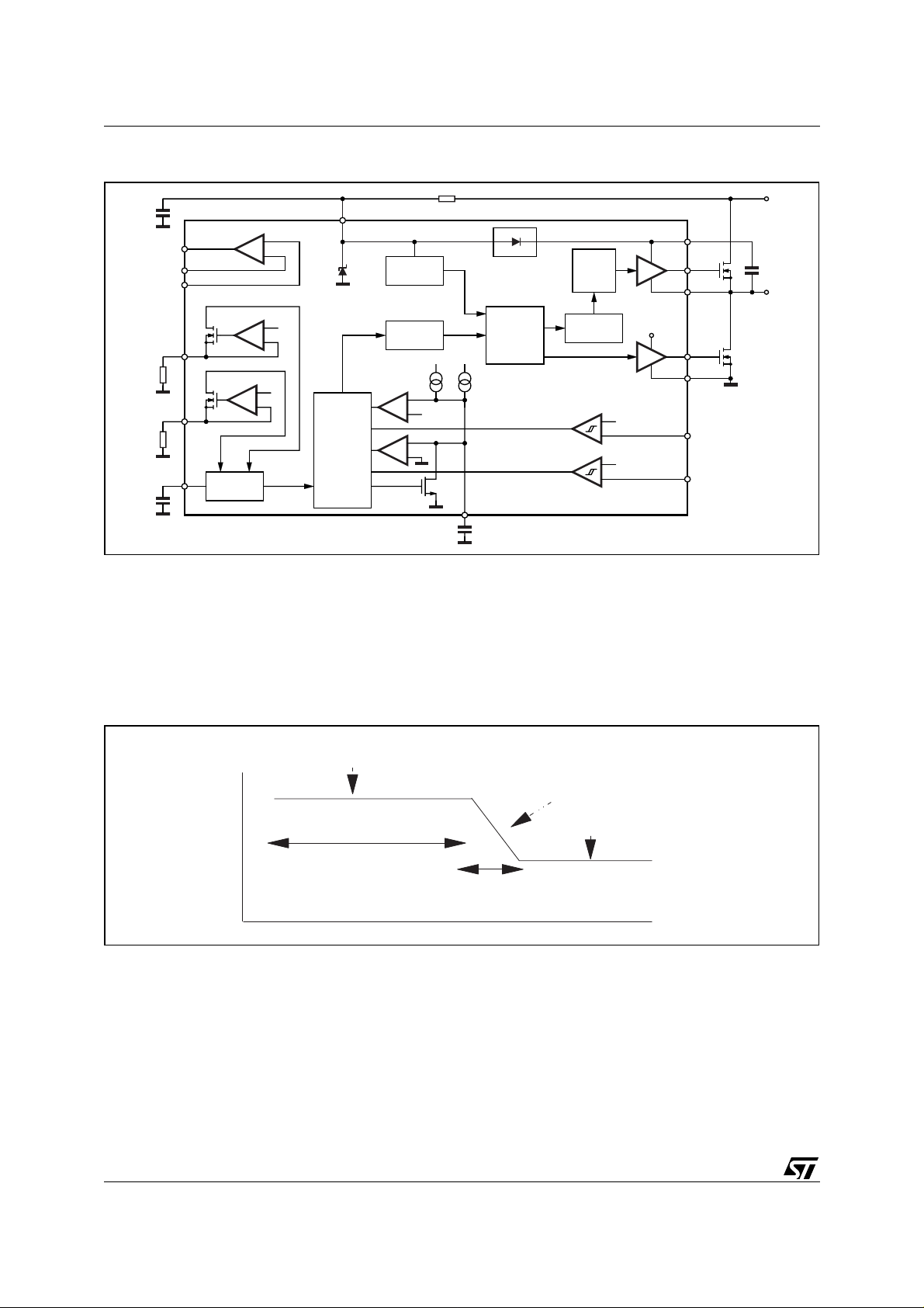
L6574 is a BCD off line 16 pin IC specifically designed for ballast applications [r ef.1](see fig.1). It has both driver
functions and controller functions on board.
The most useful characteristics to control the lamp are:
■
Preheat and frequency shifting timing
■
Cmos shut down input
■
Sense op-amp for closed loop control or protection failures
The parameters of the application are set by external components (resistors and capacitors) connected to the
IC. L6574 allows the user to set all the parameters according to the lamp characteristics, and the ballast wi ll be
a high performance one. There is a specific application note on this IC (ref. [2]) : here you find the description of
58W TL ballast with PFC section. Please refer to this application note and to the L6574 datasheet for the IC
details. In the following paragraphs we will focus our attention on a way to interface the L6574 with the microcontroller rather than on “L6574 - stand alone” perfor mances. The aim of this “supervision” is to control the three
points mentioned above.
µ
C.
µ
C work with L6574, the feasibility of
December 2000
1/20
Page 2
AN1320 APPLICATION NOTE
Figure 1. L6574 Block Diagram
V
S
OP AMP
5
OPOUT
6
OPIN-
7
OPIN+
4
R
IGN
2
R
PRE
3
Cf
Imin
Imax
VCO
+
-
V
REF
V
REF
12
CONTROL
LOGIC
UV
DETECTION
DEAD
TIME
Ifs
+
Vthpre
-
+
-
Ipre
BOOTSTRAP
1
C
PRE
DRIVER
DRIVING
LOGIC
HVG
DRIVER
LEVEL
SHIFTER
LVG DRIVER
+
-
+
-
V
V
THE
V
THE
D97IN493B
V
16
BOOT
HVG
15
OUT
14
S
LVG
11
GND
10
8
EN1
9
EN2
H.V.
C
BOOT
LOAD
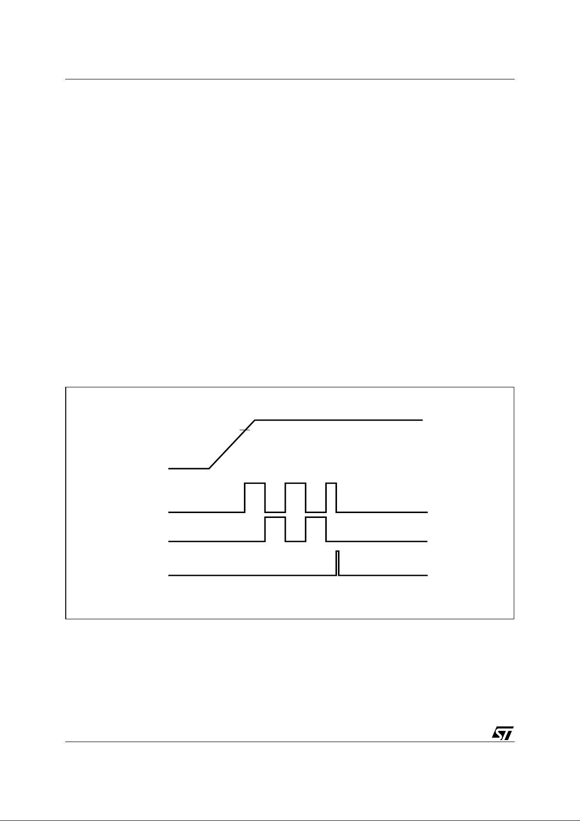
3.0 L6574: HOW TO SET FREQUENCIES, TIMING, FAULT SIGNALS IN AN “ANALOG APPLICATION”
In this paragraph we will have a snap shot of the L6574 working, just as far as the characteristics important for
the micro interface are concerned. For further details please refer to [1] and [2].
The L6574 typical behavior is shown in fig. 2: there is a starting frequency (f
set preheat time T
, than there is a frequency shift towards f
PRE
that last 0.1 of T
min
MAX
or f
PRE
) that is constant for a
PRE
and is called T
IGN
or TSH.
Figure 2. Frequency shift
freq
preheating phase
fmax
Tpre
ignition phase
normal operation
fmin
Tsh
time
Leads 1, 2, 3, 4 are used to set frequencies and timing.
The capacitor connected to pin 1[CPRE] sets the preheat time:
T
= K1 · C
PRE
The ignition time, or better, the time to let frequency shift from preheat value to the min. value is one tenth of T
PRE
PRE
.
The current that charges and discharges the capacitor connected to pin 3 (CF) sets the half bridge oscillating
frequency.
The current that charges C
2/20
is set by the current that flows out from pin 2 and 4 during preheat and from pin 4
F
Page 3
AN1320 APPLICATION NOTE
alone during the on phase. As pin 2 and 4 are at 2V, the currents that flow out of them is inversely proportional
to the resistance connected between gnd and pin 2 (R
There are some useful formula:
1.41 R
ƒ
---------------------------------------------------=
min
ƒ
max
Choosing properly the resistor and the c apacitor values the designer can set the desired fr equencies and timing.
When the designer has to do another application for another lamp type, he has to change the resistors and capacitors in order to have another range of frequencies.
For protection in case of lamp failure two logic input are provided: pin8 [EN1] and pin9 [EN2]. Both are active
high, but they have different functions: when EN2 is activated it forces the IC to start again the preheat sequence. When EN1 is activated it shut down the IC until V
EN2 is usually used as “ignition fault”: if the lamp is not ignited, the preheat sequence starts again.
EN1 can be used to sense lamp removal / replacement or disconnection.
) and between gnd and pin 4 (R
PRE
+()⋅
preRign
⋅⋅
R
preRign
1.41
----------------------- -=
R
ign
Cƒ
⋅
Cƒ
is removed or until EN2 is pulled high.
CC
IGN
).
Figure 3. EN1
V
CC
LVG
HVG
EN1
V
SUVP
D97IN490
3/20
Page 4
AN1320 APPLICATION NOTE
Figure 4. EN2
V
CC
V
SUVP
f
OUT
f
PRE
f
ING
EN2
D97IN491B
t
PRE
t
SH
t
PREtSH
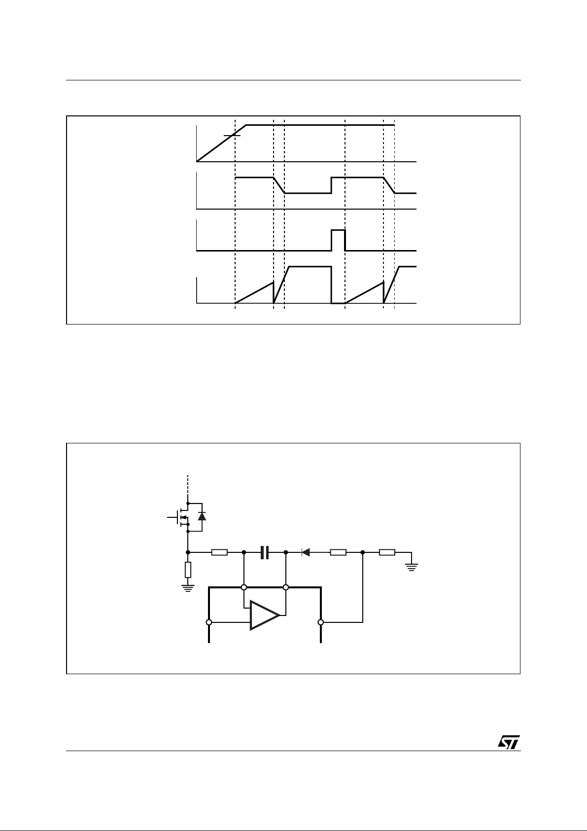
L6574 has also a sense op-amp th at can be used to have a closed loop contr ol of the lam p. We can give a voltage reference to the non-inverting input, a signal proportional to the load current to the inverting input, and we
can connect the op amp output pin to pin #4. In this way if the current in the load exceeds the reference the op
amp will sink from pin 4 an additional amount of current that has to be added to the current that flows through
R
. So the current charging CF will increase, that means a higher half bridge osci llation frequency, that m eans
IGN
a lower current in the load. C hanging the reference v oltage on the non- in verting input of the op amp we change
the frequency of the oscillator, that means we change the current in the load, and this allows lamp dimming.
Figure 5. Cl osed Loop
4/20
R25
0.68
Q3
STP4NB50/
STP6NB50
R33 9.1K
7+
C9 8.2nF
D3
1N4148
65
-
R18 100K R19 100K
RIGN
4
D98IN818A
Page 5
Figure 6. AN993 Demo Application Circuit
47K
R16 47
R20
C12
100nF
C11
680pF 630V
C20
R21
100nF
22
15
1612
2
C18
C17
L1 2.1mH
STP6NB50
Q2 STP4NB50/
R22 22
14
7
R17 9.1K
100nF 250V
R28
750K
100nF 250V
R26
390K
STP6NB50
47K
R23
11
L6574
6
C9
8.2nF
C19
8.2nF
1500V
R29
750K
Q3 STP4NB50/
D4
9
8
5
D3
1N4148
AN1320 APPLICATION NOTE
R27
6.8K
LAMP
R30
3.9K
C16 1µF
R32 20K
1N4148
R25
0.68
C15
330nF
R24
R18
100K
C14
C13
R19
6.8K
1µF
R33 9.1K
470pF
100K
10
1
3
4
D1 BYT11600
R5
T1 1.24mH (E25*13*7)
10 Turns 1.3mm gapped
R1
Bridge
Fuse
C1
220nF
DZ1
68K
1.5M
630V
D2
14V
1N4148
4.7K
RSENSE
C4 680nF
C8
R15
R12
R9
R8
C3
R2
100nF
1.5K
9.53K
0.68
0.68
10nF
10.1K
D99IN1064
R13
100K
C6
25V
R4
R3
C5
4.7µF
120K
120K
NTC
100nF
Q1
R6 22
7
8
5
6
STP6NB50
R7
47K
L6561
C2
220nF
C7
R10
400V
22µF
750K
450V
4
3
R11
12
R14
750K
5/20
Page 6

AN1320 APPLICATION NOTE
4.0 L6574: HOW TO SET FREQUENCIES, TIMING, FAULT SIGNALS IN A “MICROCONTROLLED
APPLICATION”
We have seen that the frequencies in L6574 are set by fixing the current that flows out from pin 2 and 4 and
fixing the value of the C
A microcontroller output pin can give us a high logic level (5V) a low logic one (0V) or a PWM output at fixed
frequency and variable duty cycle.
capacitor.
F
We can not use the P WM to act directly on C
pin, because the rising edge on CF is the low side mosfet “on
F
time” and the falling edge is the high side mosfet one. The half bridge would oscillate in asymmetrical way at
fixed frequency instead of at 50% duty cycle and variable frequency. So we have to interface the
pins that set the current that charges C
. A push pull output that gives us just 0V or 5V can not be used to in-
F
µ
C with th e
terface pin 2 and 4 because they have a maximum voltage level up to 2V. We have to use the integrated value
of a PWM signal to set a voltage level between 0V and 2V.
We can use a PWM output also to gi ve the op amp the vo ltage reference to c hange the load c urrent (and so the
lamp power to perform dimming)
Acting on L6574 pin 4 and (or) on pin 7 (opamp+) we can control the inverter working frequency.
If we want to control the preheat timing and frequency we have to act on pins 2 and 1. First we have to avoid
that the L6574 fixes the preheat time by itself. If we connect to pin 1 a ver y small cap (e.g. 1nF), the L6574 “analog T
” will be so small to be “invisible” to the lamp (i.e. less than 2ms). During these 2 ms, the oscillating
PRE
frequency has to be high enough to avoid lamp filaments preheat (> 150KHz). The resistor connected to pin 2
has to be sized properly.
After these 2 ms L6574 is in “working mode”: it means that pin 4 is no more involved in fixing the frequency.
Only C
Now the effective preheat time can be decided by the
and R
F
(pin 3 and 4) set it.
IGN
µ
C just acting on the PWM that gives the voltage reference
to pin 4. For example, it can have a certain duty cycle (appropriate for the preheat freq.) for a fixed time, than it
can change the duty cycle (i.e. the voltage reference) to set the ignition profile and the final working frequency.
Now we are able to change all the frequencie s and the tim ing invo lved in lamp tur ning on a nd dimming with two
connections between L6574 and the
µ
C.
The fault management can al so be d one by the
µ
C: all the fault si gnals will be br ought to it, and then it will react
according to the code. A connection that can be useful is the one to pin 8 (shut down pin) that can be direct
because the ICs levels are compatible. In this way the
µ
C can react to a signal either by stopping the inverter
or by changing the frequency (i.e. r epeating a preheat sequ ence if there is the no-i gnition al arm, or brin ging the
frequency to a very high value…).
Just with these 3 connection between the L6574 and the
µ
C we can set nearly all the parameters of the appli-
cation by software.
The number of
We need another input pin to give the
µ
C inputs we need for fault signals depends only on what we want to control.
µ
C the information about the dimming level: this is the interface between
the ballast and the “final user”. We can use either switches or an AD input. The first solution is more expensive
in terms of number of pin, the AD input requires some attention for the co de part but allows a much larger number of levels.
5.0 HOW TO APPLY THIS INTERFACE TO A BALLAST
We started from AN993 demo boar d to build a µC application with the s ame performances and s ome additi onal
degrees of freedom.
We will now apply all the concepts already discussed and put them into a working board.
6/20
Page 7

AN1320 APPLICATION NOTE
The hardware and software development can not be separated: it is a very interactive process. Starting from
the basic point there are different way to act on the L6574, depending on what we want to be softw are dependent and what we want to be hardware dependent in the final application.
We will describe the two sections separately just for ease of understanding.
5.1 HARDWARE CHOICES
First we have to choose the µC. We have chosen the ST62E62C, a 16 pin µC belonging to the ST6 family.
This device is able to perform all the functions we need with pins left over.
In this microcontroller we have just an auto reload timer, this means that we have just one PWM available. We
can call this PWM the HARDWARE PWM in the following pages, just to differentiate it from the second one we
need and that is obtained by software from a standard output pin. We will call this second PWM the “SOFTWARE PWM”
We have discussed in the previous chapters how to interface the
µ
C and the L6574; the remaining problem is
how to supply the ICs.
We have chosen a cheap way to supply the
µ
C: we use a L7805, which is a linear regulator (5V output). It has
been connected to the L6574 supply. This choice (mainly based on economical reasons) has many consequences:
■
As L6574 supply is given by a charge pump connected to the middle point of the half bridge,
the L6574 has to work (to oscillate) to give the supply to the micro
■
The ICs are not supplied at the same time, but as a sequence: the micro (the supervisor)
has to be told when everything is OK to start the preheat sequence
■
If the L6574 is disabled (after a fault condition for example) the micro no longer has a voltage
supply. When the circuit starts again the micro is reset and the program starts from the very
beginning
It can happen that the micro mus t alw ays be sup plied, even when L657 4 is off. In this case another s olution has
to be used, e.g. a regulator connected to the rectified mains.
The board start up sequence management takes into account the above mentioned point 1 and 2. Using the
start up resistors we let the L6574 start, so its oscillation allows the charge pump work. Then the L6561 is supplied and the L7805 feeds the
µ
C. This sequence is an inheritance of L6561+L6574 demo board. The co-ordination between the L6574 and the L6561 is done by choosing the start up resistors and the charge pump
components. The co-ordination between the micro and the analog part is a mix of hardware and software. By
software we let the micro w ait for a “po wer OK” signal from the L 6574, that in the meanw hile keeps on oscill ating
at a very high frequency, so as to let the filament not to be preheated. The L6574 can provide this “power OK”
signal for free. The internal sequence of the L6574 charges the preheat cap connected to pin 1 to 5V after the
preheat and the ignition sweep has ended. We can deliver this 5V signal to a
µ
C input, and hereafter the µC will
start to set all the application parameter s: in this way we are sure that everything is correctly supplied. Moreover
by choosing properly C
value (i.e. very small ~1nF) this “waiting time” is around 2 ms, so it does not influence
PRE
the overall timing: it is hundreds of time shorter than a typical preheat time.
To be sure that the third condition does not happen and that there are no out of control situations in which we
do not know which part of the code the micro is running we have added additional safety circuitry. After the alarm
for open load or disconnection, the micro sets an output pin to the high logic level in order to activate an SCR
to disconnect the VCC from all the ICs, PFC included. In this way the
µ
C can supervise not only the L6574 but
also the L6561.
7/20
Page 8

AN1320 APPLICATION NOTE
5.2 SOFTWARE CHOICES
We have already done some software choose choosing the microcontroller. When we chose a microcontroller
with only one PWM output we have already decided to devote a certain amount of microcontroller resources to
build the PWM software (see appendix for software details).
A logic sequence of actions could be:
1) to check that everything is ok - i.e. all the ICs are supplied in the right way;
2) check the presence of the load
3) do the preheat sequence
4) check lamp ignition
5) set the current in the load according to the user input
This is a basic set of functions typical of nearly any ballast application (see fig. 7)
Figure 7. Flow Chart
N
L6574 OK?
ST6 start up
Y
N
open load?
N
set Fpre
t>Tpre?
Y
set IGN freq.
profile
lamp on?
Y
set working
freq.
(freq.&loop
ref.)
Y
wait for reset
and/or pow er
off
L6574 and
L6561 disable
N
N
Y
Y
fault cd.?
N
#fail<MAX?
Y
dimming?
8/20
N
Page 9

6.0 BOARD
We have implemented the board whose schematic is shown in fig.8.
Figure 8. Schematic
PC3 (DISCONNECTED LAMP)
PC2 (NOT IGNITED LAMP)
D11
5V
R32
10K
C18
330nF
R36
6.8K
D10
1N4148
SW
S5
PB3 PO WER O K
SW
S4
S6
SW
PB2
C17
2uF
R31
20K
R33
1.2K
D9
1N4148
R35
100
IN L7805PORTR IGHT -R
R1
50
D1
D2
BRID GE
C2
R2
D4
D3
STTA106
T1
1.24mH (E25*13*7)1.3mm gapped
DIODE
-+
R17
1.2K
R10
390K
C13
1uF
R20
6.8K
8.2nF
R[*]
50K
Q2
STP6N B50
L1
2.1mH
R8
22
14
15
C3
1.34nF 600V
36
D5
14V
1N4148
D6
1N4148
R4
68K
R3
1.5M
HVG
100nF
16
VBOOT
U2
L6574
12
VS
RPRE
2
7
S1
SW
R9
81.5K
C6
100nF
C5
47uF 2 5V
Q1
R7
22
C4
10uF
7
8
VCC
GD
R6
120K
5
ZCD
U1
L6561
GND
6
R5
120K
C7
C10
100nF 2 50V
C8B1
R13
1.5M
C8
OUT
OPIN+
STP6N B50
R15
100nF 2 50V
R11
1.5M
Q3
STP6N B50
DISABLE PB0
22
11
6
S2
SW
8
9
EN1
EN2
LVG
OPOUT
OPIN-
RIGN
5
4
C9
8.2n
D7
1N4148
R16
R19
C11
47uF
R14
650K
R12
650K
4
3
1
CS
INV
2
C12
MULT
220nF 4 00V
200K
R29
R24
3.9K
R23
0.68
R28
1.2K
C16
100nF
13
NC
10
GND
1
CPRE
3
CF
C15
470pF
100K
R26
9.1K
S3
SW
9.1K
R22
8.2K
R21
0.22
R21A
0.22
R18
9.1K
R25
510K
1uF
COMP
C14
10nF
R27
10.1K
AN1320 APPLICATION NOTE
R48
100K
R46
C20
C19
1uF
321
PNP CB E
1nF
Q4
R39
R37
10K
R38
123
Q5
20K
100K
NPN CBE
R42
4.7K
R41
4.7K
NOT IGNITED LAMP
DISCONNECTED L AMP
16
PC315PC2
U3
PB01VPP2PB23PB34PB65PB7
PB7
DISABLE L6574
C22
2uF
R40
20K
R43
100K
C21
R44
2.2K
100nF
1K
C25
S7
SW
C23
20pF
C26
Y1
8MHz
10
11
12
13
14
NMI
RESET
OSC_ IN
ST62 E6 2C
OSC_ OUT
6
RIF PIN 4
PFC DISABLE
L6574 POW ER OK
RIF OP AMP (PIN 7)
C24
100nF
R47
1.5K
R45
POT 4.7K
R
10K
100nF
C27
100nF
20pF
PA49PA5
8
VSS
7
C28
VDD
2
VOUT
L7805
VIN
U4
1
C29
D13
1N4148
IN L780 5
PB6 L6561 DIS
100nF
3
GND
10uF
2A 250 V
NTC1
10
1 2
220nF 6 30V
PORTR IGHT -R
[*]: 4 resistors 200K 0.6W each
t
C1
F1
9/20
Page 10

AN1320 APPLICATION NOTE
This is a “double board”: it can be used with the micro or without it according to the position of six switches (S1
to S6) that are on board. The microcontroller, the L7805 and some parts related to the micro (the oscillator, the
reset switch and so on) are mounted on a small separated board that can be connected with a 9 pin connector
to the main board. As a result the board looks huge, but we have two di fferent applicati on on it. It is a “ modular”
board: the six switches and the small insertion PCB let the user choose between a “analog ballast” and a “microcontrolled one”.
The larger board includes the “analog ballast controller” (that is the L6561-L6574 demo board) and some additional parts that allows the use of the PCB with the microcontroller and the L7805 regulator. You can choose the
control system setting by the proper position of 6 switches:
Analog version Sw nr. Function vs. L6574
### ### SW1 Pin 2 – R
### ### SW2 Pin 8 – EN1- shut down
### ### SW3 Pin 7 – op amp ref. – PWM SW
### ### SW4 Pin 1 C
### ### SW5 Pin 9 – EN2
### ### SW6 Pin 4 – R
PRE
– power OK
PRE
- PWM HW
IGN
Changing all the switch positions the micro can take the control of the board (the control system cannot be
changed while the application is running).
The connector that allows the communication between the two boards has 9 signals:
Ref. # function Analog ↔ micro
0 Void: there is the hole but it is not connected
1GND ↔
2 PB3 (L6574 power OK) →
3 L7805 input voltage →
4 PB2 (ref. Op-amp) SW PWM ←
5 PB6 PFC disable ←
6 PB7 ref. Pin 4 = HW PWM ←
7 PC3 disconnected lamp →
8 PC2 not ignited lamp →
9 PB0 disable L6574 - EN1 ←
The two control system have the same performances, but the microcontrolled application can change its characteristics just changi ng the code of the micro. If we wish to have a counted number of re-s trike of the lamp after
ignition failure we can choose any number we want (2, 8 or 23), just chan ging a parameter of the software. The
same can be done if we connect another lamp that needs a different T
10/20
or a different range of frequencies.
PRE
Page 11

AN1320 APPLICATION NOTE
This is an added value of the micro.
An important feature of the overall ap plicati on is its modularity: we can have a boar d with th e micr o and a board
without it changing very few parts, we can also put all the parts on the same PCB and then decide which connection to do.
7.0 COMMENTS:
The lamp disconnection fault is managed as an interrupt not only for fast acting, but also for the characteristics
of the application we have chosen. The ST62E62C has just a PWM output, while the application needs two
PWM. We have solved the problem using the software PWM. This is something very “heavy” for the micro to
perform, and it influences all the other choices: e.g. a polling sequence is to expensive as time consuming and
it influences the SW PWM duty cycle dy namic. It cons umes ~25%-30% of the cycl e, and this, added to 20% due
to the 4 instructions to do the PWM itself was too large. That is the main reason why the disconnection fault is
managed as an interrupt.
Of course there ar e different solutions. A feasible choice could be to use the hardware PWM to set the reference
of the non inverting input and not to use the software PWM. But we should relay on the L6574 preheat and ignition sequence, where T
supervise less items.
PRE
, f
PRE
and T
are set by capacitors and resist ors. This means that the µC has to
IGN
A third choice might be to choose a
teristics and the
µ
C has an easier code to run.
µ
C with two PWM output: in this way the application has the same charac-
8.0 REFERENCES:
1] L6574 datasheet
2] AN993: electronic ballast with PFC using L6574 and L6561
3] ST62E62C datasheet
9.0 APPENDIX:
1) Flow Chart
2) Vardef.inc
3) Ballast.asm
11/20
Page 12

AN1320 APPLICATION NOTE
9.1 APPENDIX 1: Flow Chart
Figure 9. Appendix 1: Flow Chart
N
PB3 H?
["check
power"]
Y
check PC3:
N
["start up
sequence"]
set pwm on
PB7=duty_pre
t>Tpre?
["call tpre"]
N
set IGN freq. profile
["load duty cycle
values from look up
table"]
ST6 start up
Y
H?
wait for reset
and/or power
off
Y
PB0 & PB5 high
N
12/20
check PC2: H?
N
enable pwm1
on PB7 and
pwm2[software]
on PB2
Y
nr tent = max
Y
check PA4
voltage<>
5V
tent ?
N
Y
Y
interrupt s on
PC3?
N
Page 13

9.2 Appendix 2 - Vardef.inc
;****************** ****************** *****************************************
;
; MODULE Name: VarDef.Inc
;
;*****************************************************************************
; *** Default duty cycle value for preheating
DUTY_PRE .EQU 0BEh
; *** Maximum start-up sequence retrials
MAX_TENT .EQU 3h
; *** Default Sw PWM Duty Cycle
DEF_SW_DUTY.EQU 0BCh
; *** Gen waiting timer parameters
; Gen Waiting = 2ms
; GenTick = 11 -> 11*192us = 2.112 ms
; GenRep = 1
GenTick .equ 0Bh
GenRepeat .equ 01h
; *** Tpre waiting timer parameters
; Tpre [0.5 ./. 2 sec] = 1 sec
; TpreTick = 256 -> 256*192us = 49.152 ms
; TpreRep = 21 -> 21*49.152ms = 1.032 s
TpreTick .equ 0FFh
TpreRepeat .equ 015h
AN1320 APPLICATION NOTE
; *** Tign waiting timer parameters
; Tign [(100 ./. 200)/64 msec] = 150/64 msec = 2.34 ms
; TignTick = 12 -> 12*192us = 2.3 ms
; TignRep = 1
TignTick .equ 0Ch
TignRepeat .equ 01h
; *** Tad waiting timer parameters
; Tad = c.a 500 ms
; TadTick = 256 -> 256*192us = 49.152 ms
; TadRep = 10 -> 10*49.152ms = 491 ms
TadTick .equ 0FFh
TadRepeat .equ 0Ah
.ORG 0F00H
; Look-up table for PWM
; *HW* *SW*
.BYTE 0BCH,0B4H ; Samp = 0
.BYTE 0C1H,0C8H
.BYTE 0C2H,0CBH
.BYTE 0C4H,0CEH
.BYTE 0C6H,0D2H
.BYTE 0CBH,0DBH
.BYTE 0D0H,0E6H
.BYTE 0D5H,0FEH ; Samp = 7
13/20
Page 14

AN1320 APPLICATION NOTE
9.3 Appendix 3 - ballast.asm
;****************** ****************** ************************************** ***
;
; MODULE Name: Ballast.asm
;
;*****************************************************************************
.romsize 4
.vers "st6262"
.input "ST626x.INI"; ST626x data space & registers declaration
.input "VarDef.inc"
;==========================================================
; Data Variables
;==========================================================
Step .DEF 084H,0FFH,0FFH,M
Repeat .DEF 085H,0FFH,0FFH,M
NrTent .DEF 086H,0FFH,0FFH,M
Media .DEF 087H,0FFH,0FFH,M
Count .DEF 088H,0FFH,0FFH,M
Sample .DEF 089H,0FFH,0FFH,M
;==========================================================
; Ignition Sweep PWM Parameters
;==========================================================
.ORG 0F40H
.BYTE 0BEH,0BEH,0BEH,0BFH,0BFH,0BFH,0C0H,0C0H
.BYTE 0C0H,0C1H,0C1H,0C1H,0C2H,0C2H,0C2H,0C3H
.BYTE 0C3H,0C3H,0C4H,0C4H,0C4H,0C5H,0C5H,0C5H
.BYTE 0C6H,0C6H,0C6H,0C7H,0C7H,0C7H,0C8H,0C8H
.BYTE 0C8H,0C9H,0C9H,0C9H,0CAH,0CAH,0CAH,0CBH
.BYTE 0CBH,0CBH,0CCH,0CCH,0CCH,0CDH,0CDH,0CDH
.BYTE 0CEH,0CEH,0CFH,0CFH,0D0H,0D0H,0D1H,0D1H
.BYTE 0D1H,0D2H,0D2H,0D2H,0D3H,0D3H,0D3H,0D3H
;==========================================================
; Inizialisation
;==========================================================
.org 880h
Init
; *** Oscillator and internal Timer
; *** Port configuration
; Port A: All Input, No Interrupt, Pulled up, except PA4 Analog - PA4 = A/D (in), PA5 = N/C
; Port B: port 2,6 and 7 output 0, push pull, value 1; port 3 input
; PB0 = 6574 Disable PB2 = SW PWM (out), PB3 = POWER OK (in),
; PB6 = PFC Disable (out), PB7 = HW PWM - AutoReload Timer (out)
14/20
reti
clr IOR ; Disable Interrupts (Confirm Reset Value)
ldi OSCR,08h ; Set Prescaler ratio @ 1
ldi TSCR,27h ; Timer1 no int, presc 128, lock
ldi DRA,10h
clr DDRA
ldi OPRA,10h
clr DRB
ldi DDRB,0C5H
ldi OPRB,0C5H
Page 15

AN1320 APPLICATION NOTE
; Port C: All Input, No Interrupt, Pulled up (PC2 = NO IGN(in), PC3 = DISC LAMP (in))
; Data Rom Window Configuration
; Default Duty Cycle value on SwPWM
; A/D Converter setup
; AR-TIMER Configuration (HwPWM)
;==============================================
; Startup Sequences
;==============================================
CheckPower
; "Power Ok" test twice
clr DRC
clr DDRC
clr OPRC
ldi DRWR,3DH ; = (0F40H >> 6)
ldi V,DEF_SW_DUTY ; V = Duty Cycle
set 2,DRB ; SwPWM Port Set
ldi ADCR,10h ; AD w/out Interrupt, Turned On
ldi ARMC,20h ; Autoreload mode, enabled, stopped, no int enabled
ldi ARLR,00h ; LOAD REGISTER
ldi ARRC,80h ; RELOAD REGISTER
ldi ARCP,DUTY_PRE ; COMPARE REGISTER
set 7,ARMC ; Load ARRC and RESET ARSC1
res 7,ARMC ; STOP Load phase
ldi ARSC1,60h ; Fint, prescaler /8 Fpwm =7.8125KHz
set 6,ARMC ; Start Timer
jrr 3,DRB,CheckPower ; wait for pin = 1
ldi a,GenTick ; Load tick counter
ld x,a
ldi a,GenRepeat ; Load repetition time
ld y,a
call Wait
jrr 3,DRB,CheckPower ; test for pin data steady
LampOK ; *** Test if Lamp is connected
jrr 3,DRC,StartHeat ; if connected, go ahead
ldi a,GenTick ; Load tick counter
ld x,a
ldi a,GenRepeat ; Load repetition time
ld y,a
call Wait ; Wait
jrr 3,DRC,StartHeat ; test twice for steady
jp StopIt ; unconnected lamp: RIP
StartHeat
clr NrTent ; Reset Tentative counter
PreHeat
; *** Preheating waiting time
ldi A,DUTY_PRE ; Set preheating Duty-Cycle
ld ARCP,A
ldi a,TpreTick ; Load tick counter
ld x,a
ldi a,TpreRepeat ; Load repetition time
ld y,a
call Wait
15/20
Page 16

AN1320 APPLICATION NOTE
IgnStart
; *** Ignition sequence
clr Step ; Reset lookup table index
Ignition
Ignited
GotoStop
ldi A,40H ; Load Duty-Cycle value from look-up table
add A,Step
ld X,A
ld A,(X)
ld ARCP,A ; on comparator value
ldi a,TignTick ; Load tick counter
ld x,a
ldi a,TignRepeat ; Load repetition time
ld y,a
call Wait
inc Step ; Update step counter
ld A,Step
cpi A,40h ; if last value in table
jrz Ignited ; exit
nop ; else next value
nop
jp Ignition
inc NrTent
ldi a,GenTick ; Load tick counter
ld x,a
ldi a,GenRepeat ; Load repetition time
ld y,a
call Wait
jrr 2,DRC,LampOn ; if lamp ignited (PC2=0) go ahead
ld A,NrTent
cpi A,MAX_TENT ; if trial number overflows, stop
jrz GotoStop
jp PreHeat ; else retry
jp StopIt
LampOn
; *** System working, set interrupt on PortC, pin 2 and 3
clr IOR
clr DDRC
ldi OPRC,08H ; PC3 (No Lamp) INT pull-up
clr DRC
ldi IOR,30h ; enable global int, rising edge
; *** Internal timer activation for A/D tracking
; New Data Rom Window Configuration
16/20
res 3,TSCR ; Stop Timer 1
set 6,TSCR ; Enable interrupt
ldi a,TadTick ; Load tick counter
ld TCR,a
ldi a,TadRepeat ; Load repetition time
ld Repeat,a
set 3,TSCR ; Start Timer
ldi DRWR,3CH ; = (0F00H >> 6)
Page 17

;==============================================
; Main loop
;==============================================
res 0,ARSC0
nop
Main
jrr 0,ARSC0,Main
res 0,ARSC0
set 2,DRB ; Set SwPWM output
AN1320 APPLICATION NOTE
SwPWMLoop
;==============================================
; Routines
;==============================================
;==============================================
; Stop all operations and disables chips
;==============================================
StopIt
RIP
; =============================================
; Wait: holds for a time:=x*y*192us
; x = 192us Ticks number to hold
; y = Repeat Times
; =============================================
Wait
WaitRestart
WaitTimerExp
ld A,ARLR
cp A,V
jrc SwPWMLoop
res 2,DRB ; Reset SwPWM output
jp Main
set 0,DRB ; Disable 6574
set 6,DRB ; Disable PFC
jp RIP ; Do nothing
ld a,y ; Load repeat time nr.
ld Repeat,a
ld a,x ; Load Counter Value
ld TCR,a
set 3,TSCR ; Timer start
jrr 7,TSCR,WaitTimerExp
res 7,TSCR ; Timer expired, reset flag
dec Repeat
ld a,Repeat
jrnz WaitTimerExp ; WaitAgain
res 3,TSCR ; Repetition Timer expired, reset
ret
;==========================================================
; Setup A/D Converter
;==========================================================
SADC
clr Media; Reset Media register
ldi Count,04h ; Init counter
set 5,ADCR ; start a/d conversion
nop
nop
set 7,ADCR ; Enable Interrupt
ret
17/20
Page 18

AN1320 APPLICATION NOTE
;==========================================================
; Interrupt routines
;==========================================================
; *** Port A ; Unused
IPA
reti
; *** Port C ; Test if some signal went up
IPC
PC2End
PC3End
ld W,A ; save accumulator
jrs 2,DRC,PC2 ; Test port C, pin 2
jrs 3,DRC,PC3 ; Test port C, pin 3
ld A,W ; restore accumulator
reti
PC2 ; PC2 issued
PC3
;==========================================================
; DispatchIRQ4: test if timer or AD interrupt
;==========================================================
DispatchIRQ4
;==========================================================
IADC
nop
nop
jrr 2,DRC,PC2End ; Confirm steady on pin
jp StopIt ; Stop operations
nop
nop
jrr 3,DRC,PC3End ; Confirm steady on pin
jp StopIt ; Stop operations
jrs 7,TSCR,ITIM ; Test for timer interrupt
jrs 6,ADCR,IADC ; Test for AD interrupt
reti
res 7,ADCR ; Disable Interrupt
ld a,ADR ; Load Sample
ld Sample,a
ld a,Count ; Test for maximum sample
jrnz Conversion ; maximum reached
reti
Conversion
18/20
ld a,Sample ; a = Sample
rlc a ; a = a >> 4
rlc a
rlc a
rlc a
andi a,07h ; 8 levels
add a,Media
ld Media,a
dec Count
ld a,Count
jrz SetSamp
set 5,ADCR ; Enable A/D converter
nop
Page 19

nop
set 7,ADCR ; Enable Interrupt
reti ; Restart fo new sample
SetSamp
ld a,Media ; Media=+last 4 conversion
andi a,01Ch
rlc a
rlc a
rlc a
rlc a
rlc a
rlc a
rlc a ; sample=media/4 (media >> 2)
ld Sample,a
rlc a ; offset for table look-up (@ 0x40)
addi a,040h
ld x,a
ld a,(x)
ld ARCP,a ; hw pwm
inc x
ld a,(x)
ld v,a ; sw pwm
reti
;==========================================================
ITIM
ldi a,TadTick ; Load tick counter
ld TCR,a
res 7 ,TSC R ; Reset Tout Flag
dec Repeat
ld a,Repe at
jrnz GetOut ; WaitAgain
res 3,TSCR ; Repetition Timer expired, reset
call SADC
ldi a,TadRepeat ; Load repetition time
ld Repeat,a
set 3,TSCR ; Start Timer
GetOut
reti
AN1320 APPLICATION NOTE
;==========================================================
ARTInt reti ; Autoreload Timer interrupt
INMI RETI ; not used
.org 0FF0H
irq4
jp DispatchIRQ4
irq3
jp ARTInt
irq2
jp IPC
irq1
jp IPA
.block 4
nmi
jp INMI
vrst
jp Init
.END
19/20
Page 20

AN1320 APPLICATION NOTE
Information furnished is believed to be accurate and reliable. However, STMicroelectronics assumes no responsibility for the consequences
of use of such information nor for any infringement of patents or other rights of third parties which may result from its use. No license is granted
by implic ation or otherwise under any patent or patent r i ght s of STMi croelectr oni cs. Specifications menti oned in thi s publication are s ubj ect
to change without notice. This publication supersedes and replaces all information previously supplied. STMicroelectronics products are not
authorized for use as cri tical components in li f e support dev i ces or systems without express writ t en approval of STMicroel ectronics.
The ST logo is a registered trademark of STMicroelectronics
2000 STMi croelectronics - All Ri ghts Rese rved
Australi a - Brazil - China - Finland - Fr ance - Germany - Hong Kong - India - Italy - Japan - Malaysia - Mal ta - Morocco - Singapore - Spain
STMicroelectronics GROUP OF COMPANIES
- Sweden - Sw itzerland - United Kingdom - U. S .A .
http://www.s t. com
20/20
 Loading...