

Page 1

AN1317
®
- APPLICATION NOTE
NON ISOL ATED POWER SUPPLIES IN BUCK AND
INVERTER CONFIGUR ATION USING VIP e r2 0 DEVICE
A. Bailly - S. Luciano
INTRODUCTION
The VIPer20 is a full integrated switching device. It replace s the con ventional PWM driver circuit, its
associated high voltage Power MOS FET switch and a full set of other passive com ponen ts, and provi de
a high level of performance thanks to its current mode structure and standby operation capability.
1. SCOPE
The VIPer20 is initi all y de sig ned to be used at the pri m ary si de of an y off line po w er supp lie s in isolated
flyback configuration but it is also the right solution for different types of not isolated power supplies
applications whe re low power (1W to 5W) , wide input vol tage range and low price s are requi red. In this
case, a simple two pins inductor can replace an expensive safety transformer. The basic principle of this
type of supplies is to convert a high voltage source to a low voltage one by the only way of the switching
frequency and duty cycle management.
The applications like home appliances (microwave oven, washing ma chine, triac drivers...), industrial
applications (motor s control,...) do not require galvanic isolation between the mains lines and the low
voltage load, especia lly when one of the low voltage outputs must be connec ted to one of the mains
line s.
All these applications will take benefits from VIPer20 features:
• Full integrate d PWM start up cu rrent source and high voltage Po wer MOSFET, allow to build simple,
robust, cost effective and compact power supplies.
• Built in overtemperature and overcurrent protection provide a safe control in overload conditions.
This application note gi ves al l the ele ments to ena ble th e designer to s tart the d evelopment of his own
non isolated power supply using the VIPer20. It defines the key components, and highlights the
differences between the Buck and the Inverter (also called Buck-Boost) topologies.
2. NOT ISOLATED TOPOLOGIES
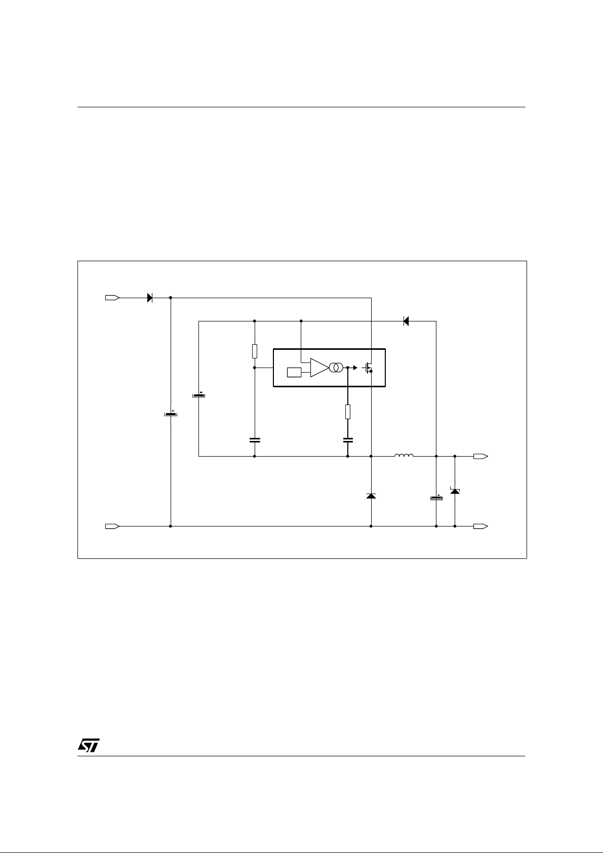
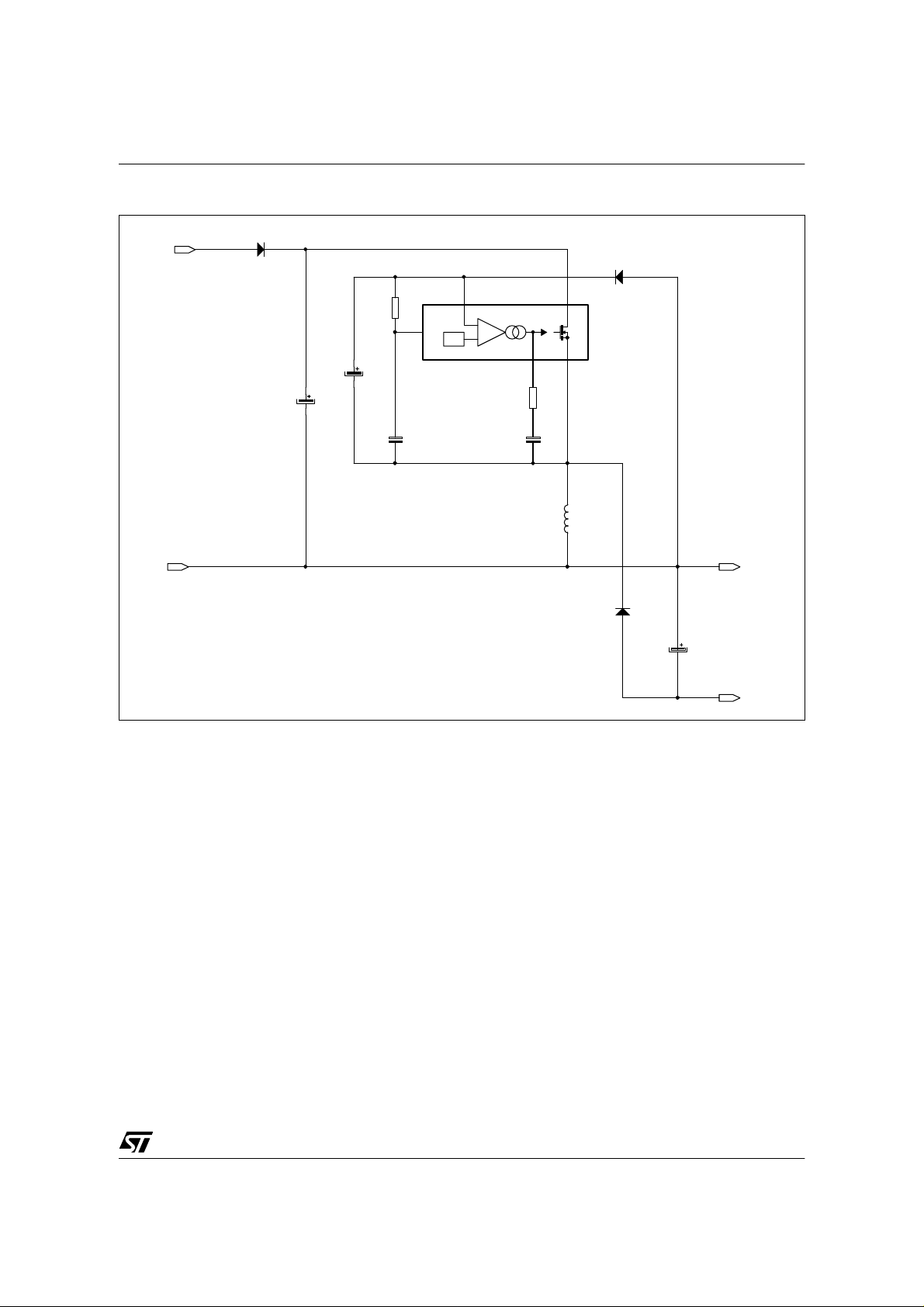
2.1 VIPer20 In Buck Topology
The basic schemati c of a VIPer20 in Buck topology deli vering 2W typi cal, with a fixed outp ut voltage, is
given fig. 1. T he Buck structu re is compos ed her e by the o n chip Power MO SFET, the ind uctor L1, the
free wheeling diode D3, the output filtering capacitor C5 and the output load itself.
In this topology, the VIPer20 switching duty cycle is very low (a few percent) because of the very high
difference between the input and t he output voltages. Its value w ould be at the maximum equ al to the
voltages ratio, when in continuous mode and even less in discontinuous mode. If the switching frequency
is too high, the Power MOSFET conduction time will decre ase accordingly, which may result in early
burst mode operation if lower than the minimum turn on time of the device. In practice, the chosen
Janua ry 20 01 1/23
Page 2
AN1317 - APPLICATION NOTE
switching frequency will be comprised between 20 kHz and 30 kHz, just above audible values.
During the star t up phase, the V IPer20 is i n standby mode and i ts on chip high voltage current source
sources a cur rent o n the VDD pin until the volt age a cross the capacitor C2 reaches th e V
Then, this current sou rce is turned off and the device starts switching. After a transition phas e during
which the output voltage grows up, the VDD supply of the VIPer20 is provi ded by the capacitor C2 and
finally, from the positive out put throug h the diode D2 when the outpu t voltage b ecomes highe r than the
current VDD value.
Figure 1: 2W typical single output not isolated power supply with Buck topology
DDon
threshold.
AC IN
AC IN
D1
1N4007
C1
22uF
400V
C2
10uF
16V
R1
10k
C3
10nF
OSC
VIPer20
D2
BYT01-400V
DRAINVDD
-
13V
+
COMP SOURCE
R2
3.9k
C4
100nF
BYT01-400V
D3
L1
470uH
C5
33uF
16V
+13V
DZ1
BZX55C15V
GND OUT
In normal operation, the output voltage regulation is achieved by the VIPer20 error amplifier which
accurately compares the VDD value to the internal 13V voltage reference. The forward voltage across the
diode D2 is here partially compensated by the forward voltage across the diode D3. So, the output
voltage and the on chip voltage refer ence val ues ar e equal, exc ep t for diode for ward vol tage differences
due to different dio des cur rent : It is g ener al ly hi ghe r in th e fr ee w hee ling di od e D3, r esul ting i n a sligh t ly
lower output voltage.
A typical characteristic of the Buc k is that the inductor cha rge and discharge paths a re exclu s ivel y done
through the output load. It is a slight advantage i n norma l operation because the energy is transferre d to
the load during both turn on and turn off cycles, but in very low or no load conditions, it has two
drawbacks:
• The charge of the star t up tank capacitor C2 is imp ossibl e, especial ly when the input v oltage is slow ly
2/23
Page 3
AN1317 - APPLICATION NOTE
increased. If no protecti on is fores een, it is p ossible to ap ply the inpu t voltage dire ctly on the outp ut,
with large overvoltages.
• Once started, overvoltages may also occur at the output, mainly for low input voltage values.
The root cause of the last phenomeno n resides in the duty cycle i ncrease at low input voltage, togethe r
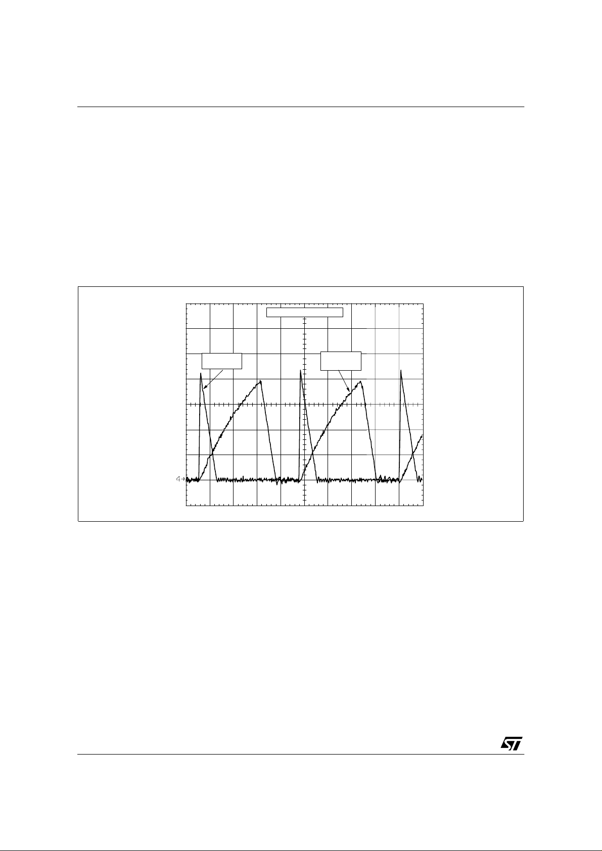
with a low output load. Fig. 2 shows the drain current shape for two input voltages. The lower is the input
voltage, and the hi gher is the turn on . As a consequ ence, the tur n off phase du ring which t he energy is
sent to C2 through D2 i s reduced, and the device is increasi ng its drain current to maintain a correct
regulated vo ltage on the VDD pin at 13 V. If the load is not a ble to absorb the corresponding curre nt
during the on phase, overvoltage is resulting on the output.
Figur e 2: Drain current for two input voltages in low load conditions
50mA/Div - 10µs/ Div
Vin = 200V
Iout = 5mA
Vin = 50V
Iout = 5mA
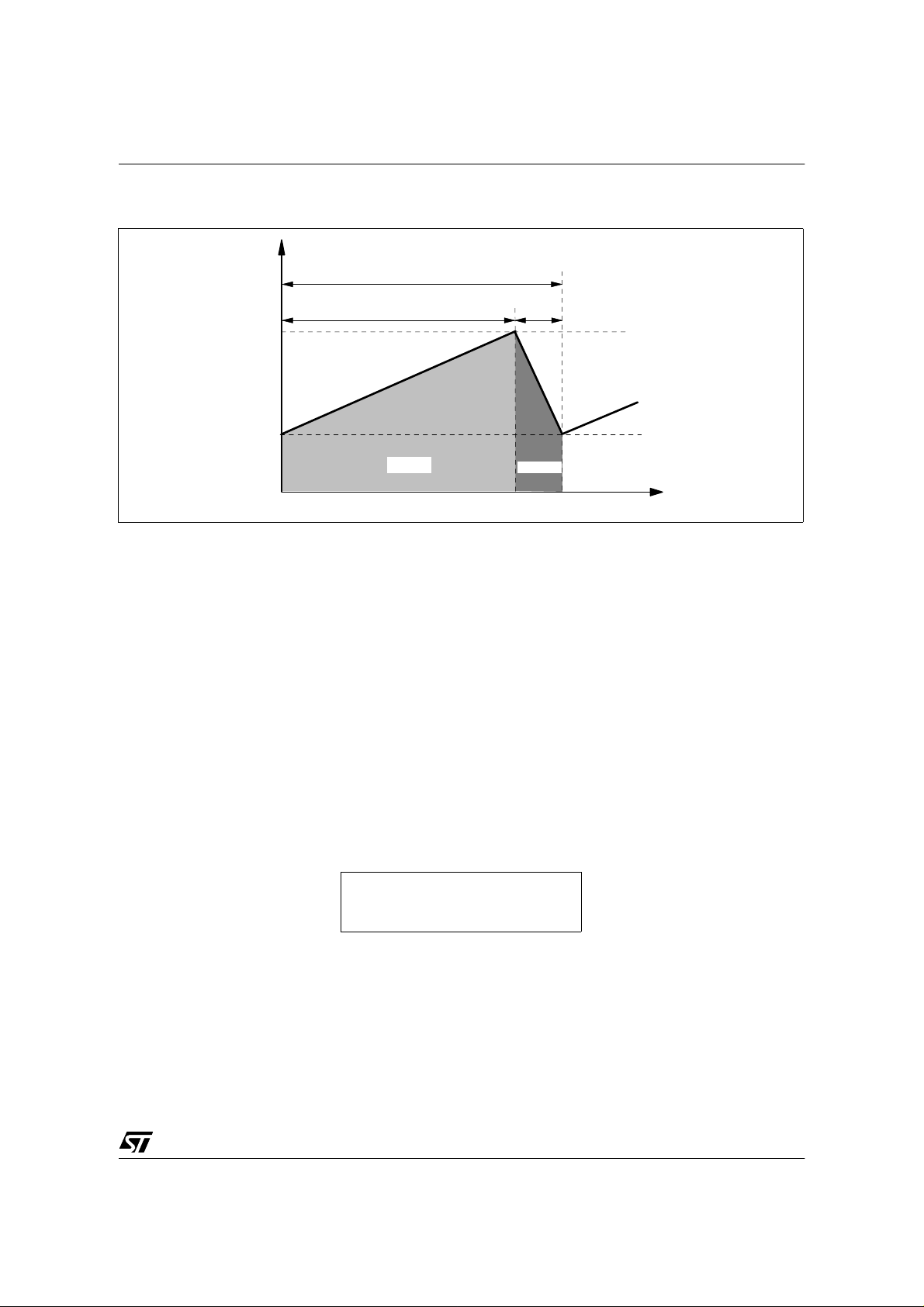
Fig. 3 shows an extreme case where the phenomenon reaches its critical phase, with a continuous mode
of operatio n. The followi ng compu tation d emonstrate s the ri sk of overvolt age an d/or over current on t he
output.
3/23
Page 4
AN1317 - APPLICATION NOTE
Figure 3: Switching cycle in continuous mode in low input voltage condition
I
DRAIN
T
s
Ts
tON
I
P
PP
I
0
- ton
Charge
The average currents consumed by the VIPer20 I
1
DD
------------2T
⋅
+()T
I
PI0
s
I
and the output current I
DD
t
–()⋅⋅=
S
on
Discharge
t
can be expressed as:
out
and
out
------------2T
⋅
+()t
⋅⋅=
I
pI0
s
on
I
1
By using these two equations:
I
DD
I
out
Finally, by introducing the duty cycle expression in continuous mode:
t
on
----------------- -
⋅=
Tston–
t
on
------
==
d
T
s
V
---------- V
out
in
The minimum output current mandatory to keep the output voltage under control is given by:
V
out
-------------------------
out
I
DD
⋅=
VinV
–
out
I
To prevent th es e distur banc e s resul ting i n possi ble o utput overvoltage or incor rec t start up, a 1 5V ze ner
diode DZ1 is added . It allows a curr ent to flow at the output, insur ing a corr ect start up and cl amps any
possible overvol tage. Nev ert heless , as show n in the abo v e last formula, the current flowi ng in this zener
can be very high when the input voltage approaches the output one. Sectio n 5 describes a schematic
modification to overcome this issue.
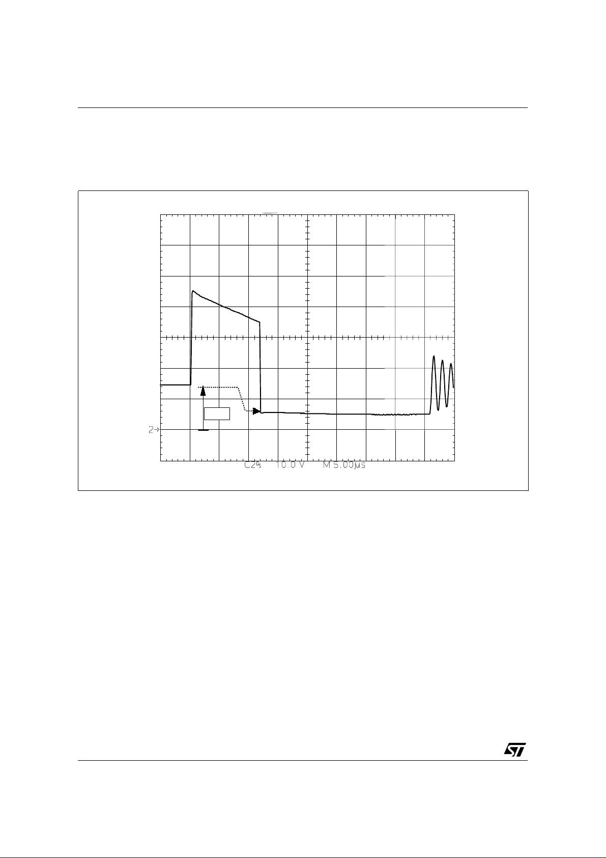
Fig. 4 presents the operation of the free wheeling diode in this condition: Actually it is always blocked, as
the voltage on the cathode never becomes negative. Also on this figure, it can be observed that the
voltage drop Vd across D3 is about 5V while the output voltage is at 15V. It means that VDD is about 10V
4/23
Page 5
AN1317 - APPLICATION NOTE
because the input v o ltage is to o low to i nsure a prop er ope ration of the con verter, which is about to sh ut
down.
Figur e 4: Buck non isolated - VIPer20 source voltage with VIN = 47 V, I
Vd
=5 mA. DZ1 conducting
OUT
2.2 VIPer20 In Inverter Topology
The inverter sche matic is derive d from the Buck one of fig. 1 by just swapping the in ductor L1 and the
free wheeling diode D3. The resulting schematic is given fig. 5. There is a major difference with the Buck
from a functional point of view : when the on chip Power MOSFET is turned on, the inductor L1 does not
charge anymore through the load but betwee n the mains lines. The out put load now gets all its energy
during the MOSFET off state, through the inductor L1 and the free wheeling diode D3.
As a consequence, the zener diode DZ1 is no more necessary because of two reasons:
• The charge of the tank capacitor C2, now independent from the load, is always possible.
• Both VIPer20 supply (VDD pin) and output load are re ceiving ene rgy form the ind uctor L 1 at the same
period of time. So, there is no possible difference between the VDD voltage and the output one, which is
always under control.
Compared to the Buck, the current flowing through the load is in the opposite direction so that the output
voltage beco mes now negati ve. As a conseq uence, the output capacitor C5 polarity m ust be swapp ed
and the anode o f the diod e D 2, supplyi ng the VI Per20, must now be connecte d to the groun d l ead GND
OUT to insure a correct positive supply to the VDD pin.
5/23
Page 6
AN1317 - APPLICATION NOTE
Figure 5: 2W typical single output not isolated power supply with Inverter topology
AC IN
AC IN
D1
1N4007
C1
22uF
400V
C2
10uF
16V
R1
10k
10nF
C3
OSC
VIPer20
D2
DRAINVDD
-
13V
+
COMP SOURCE
R2
3.9k
C4
100nF
L1
470uH
BYT01-400V
D3
BYT01-400V
C5
33uF
16V
GND OUT
-13V
3. DESIGN METHODOLOGY
The schematic of either fig. 1 or fig. 5 can be separated into six blocks:
• The oscillator network composed by R1 and C3.
• The Buck or inverter structu re, whic h is compo sed by the o n chip MOS FET, the inductor L1, the fr ee
wheeling diode D3 and the output filtering capacit or C5.
• The VIPer20 supply circuit, composed by D2 and C2.
• The front rectifier and filter.
• The error amplifier compensation network composed by R2 and C4.
All these functions will be detailed in the next paragraphs.
3.1 Switching Frequency And Duty Cycle
Sections 1 and 2 showed that the input voltage transformation is entirely managed by the VIPer20 which
controls the switching duty cycle. Whatever the topology is, the goal is to look for the widest load
regulation range, trying to reach the VIPer20 minimum turn on time (T
= 500 ns typ.) for the lowest
ONmin
output load. For maximum load, although the VIPer20 is perfectly compatible from the continuous mode,
it must be avoided becaus e the power dis sipation in the fre e wheeling di ode D3 would be too high and
the inductor s ize a nd price would inc re ase. F or all the above rea s ons, th ese topologies are ope rated at
6/23
Page 7

AN1317 - APPLICATION NOTE
dtonFs⋅=
low switching frequency and always in discontinuous mode.
As an example, to get a 13V output voltage with a 265 Vrms input voltag e, the maximum duty cycle
V
out
---------- -
d
=
time would always be equal or lower than T
practice the switching frequency is chosen just above the audio ones, in the 20 kHz to 30 kHz range and
the VIPer20 will work in discon tinuou s mod e with a d uty cycle of a bout 2% to 3% at h igh line and abo ut
6% to 10% at low line.
From the VIPer20 datasheet, the switching frequency is given here below:
would be l ess than 5%. With a switch ing frequency of 100 kHz, the maximum c onduction
V
in
, leading to a permanent burst mode operation. In
ONmin
2.3
---------------- -
F
s
R
1C3
On the schema tic of fig. 1 and fig. 5, R1=10kΩ and C3=10nF have been chosen to get a switch ing
frequency near by 20 kHz (21.7 kHz typical).
3.2 Inductor
In normal o peration, for both topologies, the switching cycle consists of tw o phases. First, the Power
MOSFET is switch ed on during ton, D3 is blocked, the i nductor connected to the high v oltage source
stores the energy. Second, the Power MOSFET is switched off during t
energy to the load through D3, and to the VDD pin through D2. As described in section 2, th e load is
supplied du ring t
switching cycle is shown on fig. 6.
Knowing the ou tput power, the switching frequenc y and the m aximum VIP er20 peak cu rren t, L1 can be
computed as follow:
for the Buck:
with and
on
and t
dis
P
out
with the Buck top ology, a nd only during t
1
2
-- -
I
out
F
p
L
1
2
tonVinV
–()L
⋅=
⋅
1
-- -
I
s
pVout
2
I
⋅=
1
550
---------------------
1
–
R1150–
dIDDV⋅
p
, the inductor restores its
dis
with the inverter o ne. A typical
dis
–⋅⋅+⋅⋅=
out
7/23
1
out
-- -
L
2
L
1
P
1
2
I
p
2
Fs1
--------------------------------------------------------------
⋅=
2
I
p
-------------------------
+
VinV
P
+
outIDD
Fs1
⋅⋅
V
out
–
out
V⋅
V
-------------------------
+
VinV
–
–⋅⋅⋅=
I
DD
out
out
out
V⋅
out
Page 8

AN1317 - APPLICATION NOTE
Figure 6: Switching diagram in normal operation (discontinuous mode)
DRAIN
I
T
s
tDis
t
ON
IP
Charge Discharge
t
OFF
t
1
out
-- 2
for the Inverter:
P
2
I
FsI
p
L
1
–⋅⋅=
2
L
1
V⋅
DD
out
P
+
outIDD
-----------------------------------------
⋅=
2
Fs⋅
I
p
V⋅
out
In practice, with a less than 10% error, the VIPer20 consumption and also the power transferred to the
load during the conduction time of the MOSFET for the Buck (Vin»V
) can be neglected. In this case,
out
the calculation becomes the same for both topologies:
P
out
---------------- -
⋅≈
2
I
Fs⋅
p
=0.5A min, Fs=20kHz, it gives L
1l
800µH.
For a 2W maximum output power, with Ip=I
L12
Dpeak
The power delivered by these topologies is limited by the minimum VIPer20 current capability and by the
I
fact that continuous mode has to be avoided. The maximum output current is therefore about .
Dlim
--------------2
It gives also a maximum inductance value, for a given frequency:
V
out
L
1max
----------------------
≈
I
DlimFs
⋅
On fig. 9 and 11 of section 4, a 2 W typical out put power can be obtained with an inductor value of
470 µH (I
=0.67A typical).
Dlim
8/23
Page 9

AN1317 - APPLICATION NOTE
3.3 Output Capacitor
The output capacitor C5 is an element linked with the desired output ripple amplitude ∆V
depends on the output voltage and on the application to supply.
The worst case occurs for the maximum load, when the VIPer20 delivers its maximum peak current
during the longer conduction time. The charge of the capacitor C5 is:
, which
out
Q
With the hypothesis that the VIPer20 is at the limit of the continuous mode, which is a worst case making
easier the calculation of the current in the capacitor:
i
dt⋅
∫
Example with ∆V
The maximum peak current flowing through this capacitor is during the charge and during the
discharge . To avoi d an excess ive power dissipation in the capac itor and a hi gh out put rippl e , the ESR of
the output capacitor must be low. Table 1 gives a picture of the ESR impact, with =0.7A typical.
Table 1: Output ripple versus capacitor technology
Capacitor Type Capacitor Value ESR at 100KHz IR at 100KHz
Standard Electrolytic 33
Electro lytic Solid Al 33
Electrolytic OS-CON 33
Electrolytic Low Z 270
=100 mVpp, Fs=20 kHz, Ip=I
out
µF / 16V 7 Ω 90 mA 4.9 V
µF / 16V 700 mΩ 1460 mA 490 mV
µF / 16V 50 mΩ 1580 mA 35 mV
µF / 16V 120 mΩ 630 mA 84 mV
itd⋅ C5∆V
=
5
∫
T
I
1
s
-- -
-----
----
⋅
2
2
1
-- -
TsI⋅
8
---------------- -
C
=
5
∆ V
=0.5 A min, C
Dpeak
⋅()=
out
1
p
-- -
⋅==
T
8
p
I
p
---- 2
sIp
5l
31 µF
I
p
Output Ripple
V
R
I
p
---- -
–
2
= I
• ESR
p
2
out
The above example illustrates that the computed capacitor value has to be tuned according to the
application needs, the capacitor technology and its associated cost.
3.4 VIPer20 Supply Cir cuit
For both topologies, fig. 7 shows the three different mode:
• The start up phase: The on chip high voltage current source is turned on. It sources a current out of the
VDD pin in order to char ge the tank capacitor C2 unti l the V
then supplies the VIPer20 during the following phase.
9/23
threshold is rea ched. This capacito r
DDon
Page 10

AN1317 - APPLICATION NOTE
• A transitio n phase: It takes place i mmediately after the previo us one. The current s ource is tur ned off
and the devic e starts switch ing. At the very beginning, th e output vo ltage is lower than VDD one, the
diode D2 is blocked, the VIPer20 is still su pplied by C2. When t he output voltage, incr easing cycles
after cycles, reaches V
of C2 must be large enough to maintain th e VDD voltage above the V
supplied from the output. If it is not the case, the VIPer20 will loop into endless start up cycles.
• The normal operation: The VDD pin is fully supplied by the low voltage output and regulated at 13 V.
Figure 7: VIPer20 supply phases in Buck or Inverter topologies
V
out
V
DD
, D2 conducts, supplying the VIPer20 from the outpu t. Obvious ly, the value
DDon
threshold, before b eing
DDoff
Start up phase Transition phase
Normal operation
VDDreg
tss
VDDon
V
off
DD
tch
The calculation of the VDD tank capacitor C2 can be done as follow:
The minimum s tart up time t
must be higher than th e output capacitor C5 charging ti me tch, which is
ss
function of the nominal output voltage and the average output current:
⋅
C
5VDDo ff
tsstch>
---------------------------- -
=
I
outavg
t
During the very first start up cycles, C5 is empty, the output voltage is more or less null and the VIPer20
delivers its maximum peak current I
voltage, the inductor L1 discharges very slowly (t
mode. At that time, the average output current is almost equal to I
during the Power MOSFET on state. Due to the low output
Dlim
) so that the switching is done in continuous
dis»Ts
.
Dlim
10/23
Page 11

AN1317 - APPLICATION NOTE
0tt
ss
≤≤
t
ss
I
DDoC2
⋅
V
DDhyst
-----------------------
=
While the outp ut voltage grows up, t he disconti nuous mode is r eached and the aver age output current
becomes the half of the maximum peak current:
3
-- 4
I
Dlim
1
-- -
≈⇒=
I
2
Dlim
, and it can supply the V
DDon
DD
t0I
The average output current for can be approximate as:
At the beginning of the start up ph ase, the capacito r C2 is charge d at V
pin down to V
≈⇒=
outavgIDlim
. So, t
DDoff
and
can be expressed as:
ss
tt
ssIoutavg
I
outavg
≈
V
, with
=13V, I
C
2
=16mA, Ip=I
DD0
So:
Finally:
With: V
3.5 Front Rectifier And Filter
As single wave rectific ation is chosen becaus e it allows to have the output ground connected to one of
the mains lines, as it is required in most of the non isolated applications. As the involved power is low, the
input filtering can be achieved without huge bulk capacitor. Any usual rectification diode having a reverse
voltage of 800 V will fit the needs. On the schematic of fig. 1 and 5, we used the part number 1N4007.
The energy stored in the bulk capacitor during the conduction time of the diode must be equal to the total
power dissipated when the diode is blocked.
Referring to fig. 8 and with the efficiency of the converter , it comes:
out
DDhyst
I
⋅
DD0tss
---------------------V
DDhyst
Dlim
V
-------------------------------------------------------
I
>=
DD0
C
>
2IDD0
=0.5A min, V
–=
DDonVDDoff
3
C5V
⋅()
-- -
out
4
V
DDhyst
4C5V
⋅⋅
---------------------------------------------
⋅⋅
3I
DlimVDDh yst
=2.4V , C5=33µF, C2>7.6 µF.
DDhyst
I
⋅()⁄
Dlim
η
out
=
P
out
--------- P
in
1
-- 2
The designe r can easily choos e V
accept, knowing that a V
11/23
2
V
C
inpeak
1
2
V
–()t
inlow
reasonable value is 70% of V
inlow
1
out
---
η
inpeak
.
t
–()P
⋅⋅=
2
1
according to the inp ut v o ltage ra nge a nd the output rippl e he can
inlow
Page 12

Figur e 8: Single wave filtering
in
V
V
in
peak
DC
V
V
inlow
1
t
Ts
AN1317 - APPLICATION NOTE
t2
t
t2 and C1 can now be extracted as follow:
V
inlow
C
t
2
V
inpeak
2
1
sin⋅ t
–()P
t
2t1
-----------------------------------------------
⋅=
2
V
inpeak
-----
2π
T
s
1
⋅⋅
---
out
η
2
V
–()
low
2
, with
T
----- 2π
s
arc
V
inlow
------------------sin Ts+⋅=⇒=
V
inpeak
T
s
-----
t
=
1
4
A wide range input voltage desig n, fitting both Ameri can and European s tandards, is consi dered: The
minimum AC voltage is 85 Vrms, so V
power and he chooses V
=80% of V
inlow
=120V, 60 Hz. The designer needs a 2 W m aximum outpu t
inpeak
. Knowing that the typical efficiency η for this type of
inpeak
converter is ab out 70%, he gets C1=19.4µF. He will retain 22 µF which is t he closest higher normalized
value, with a voltage of 400 V to cover the whole range.
3.6 Compensation Network
The R2 and C4 ne twork connected on th e COMP pin of the VIPe r20 insures a correct stability o f the
converter. Note that both Buck and inverter topolog ies are worki ng in discontinuou s, and have a very
similar dynami c beh avi or. So, the values in dicated on t he schem ati cs are convenient for both topolog ie s
and in all load conditions.
12/23
Page 13

AN1317 - APPLICATION NOTE
4. MEASUREMENT RESULT S
The following grap hs show typical res ults using the schematic s of fig. 1 and fig. 5. Unless specifie d, the
measurements are done at ambient temperature.
4.1 Buck And Inverter Output Characteristics
Figur e 9: Typical output characteristic of the Buck topology
Vout (V)
16
15
14
13
12
11
10
9
8
7
0 50 100 150 200 250 300
Iout (mA)
Figure 10: Buck non isolated - Output voltage at low load and low input voltage
Vout (V)
16
14
Vin = 300V
Vin = 200V
Vin = 100V
13/23
12
10
-100mA
8
-30mA
-5mA
0mA
6
20 30 40 50 60 70 80 90
Vin (V)
Page 14

AN1317 - APPLICATION NOTE
Fig. 10 illustrates the Buck behavior in low load and low input voltage conditions, as described in section
2.1. The output voltage is clamped to 15V by the zener diode.
At the opposite, as shown in fig. 11 and fig. 12, the output voltage regulation of the Inverter is much better
whatever are the load and the input voltage.
Figure 11: Typical output characteristic of the fig. 5 Inverter schematic
-Vout (V)
14
Vin = 300V
13
Vin = 200V
12
Vin = 100V
11
10
9
8
7
0 50 100 150 200 250 300
-Iout (mA)
Figure 12: Inverter non isolated - Output voltage versus load and input voltage
-Vout (V)
15
10
5
0
0 50 100 150 200 250 300 350
Vin (V)
-100mA
-30mA
-5mA
0mA
14/23
Page 15

AN1317 - APPLICATION NOTE
4.2 Buck And Inverter Power Measurements
Figure 13: Buck non isolated - Input power versus output power
Pin (W)
4
3.5
3
2.5
2
1.5
1
0.5
0
00.51
1.5 2 2.5 3
Pout (W)
Vin = 300V
Vin = 200V
Vin = 100V
Figure 14: Inverter non isolated - Input power versus output power
Pin(W
)
3.5
3
2.5
2
1.5
1
0.5
0
00.511.52
Pout(W)
Vin = 300V
Vin = 200V
Vin = 100V
2.5
15/23
Page 16
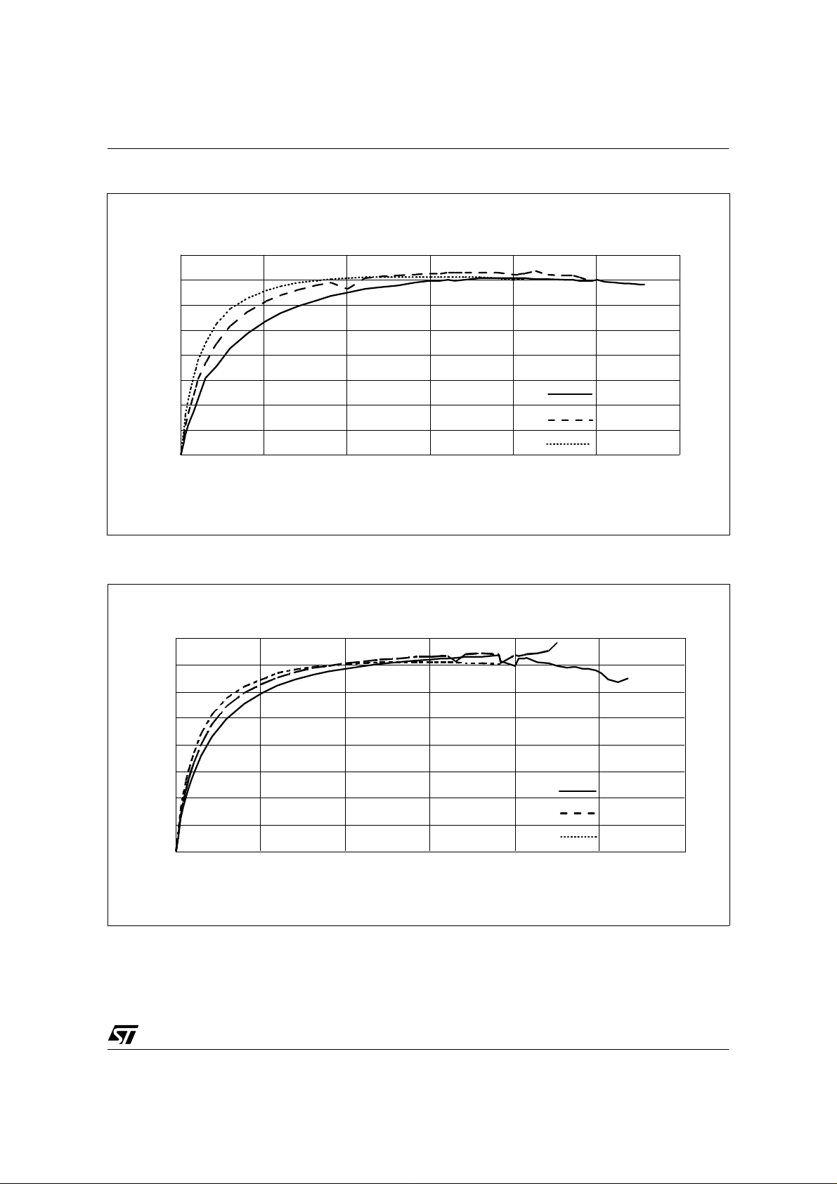
Figure 15: Typical efficiency of a Buck non isolated
Efficiency
80%
70%
60%
50%
40%
AN1317 - APPLICATION NOTE
30%
20%
10%
0%
050
100 150 200 250 300
Iout (mA)
Figure 16: Typical efficiency of an non isolated inverter
Efficiency
80%
70%
60%
50%
40%
30%
20%
10%
0%
0 50 100 150 200 250 300
-Iout (mA)
Vin = 300
Vin = 200V
Vin = 100V
Vin = 300V
Vin = 200V
Vin = 100V
V
4.3 Sh ort Circuit
Fig. 17 shows the inductor current when submitted to a short circuit on the output. It can be seen that this
current exce eds the current limitation of the VIPer2 0 (It is about 3 A for a limitation of 0. 67 A for the
16/23
Page 17

AN1317 - APPLICATION NOTE
device). This situation is due to the fact that the minimum turn on of the device is not sufficiently short to
keep the drain current under control, especially because the inductor is saturated.
Figure 17: Buck non isolated - Inductor current in short circuit condition at Vin = 400 V
Nevertheless, the device is protected against such events and can be connected directly across the front
bulk capacitor c h arge d at 40 0 V with out a ny pro bl em. Thi s corr es pon ds to th e w orst cas e of a sa turat ed
transformer, which is nev er reached p ractically. Would it happen, the re sulting pow er dissipation wo uld
be limited by the thermal shutdown of the device.
Figure 18: Buck non isolated - Short circuit output current at Vin = 400 V
17/23
Page 18

AN1317 - APPLICATION NOTE
Fig. 18 represents the ou tput short circuit curr ent. Its duty cycle is about 27% for a peak valu e of 1.4 A.
This results in an average current of 0.4 A which is perfectly compatible with the type of diodes generally
used for recti fyin g th e o utput . A ctua lly, these types o f co nverte r c an withs tand t he short ci rcuit c ond ition
indefinitely. The temperature elevation of the components is quite moderate.
5. SCHEMATICS IMP R OVEMENTS AND VARIANTS
5.1 Non Isolated Buck With Output Overvoltage Protection
The inherent inconve ni ent of the Buck, alrea dy des cribe d in paragrap h 2.1 and 4.1, is the output voltage
increase, in low load and low input voltage conditions.
On the initial schem atic of fig. 1, the zener diode properly clamps the output voltage surges when a
minimum load is guarant eed and if the input voltage rise and fall times between 20V to 50V typical, is
short enough. Otherwise, the output voltage may rise such values that the power dissipation in DZ1
becomes very high, as shown on fig. 19.
Figure 19: Buck non isolated - DZ1 power dissipation in short circuit
Pz (mW)
600
500
400
300
200
100
0
20 40 60 80 100 120
Vin (v)
The solution i mplemented on the schem atic of fig. 20, allo ws to drastically impro ve the output voltage
control, by reducing the nominal switching frequency if the input voltage decreases below a threshold.
This frequency sh ifter c o nsi sts of a di ode D4 c onn ected o n the O SC pi n o f the V IPer20, and receivin g a
fraction of the i npu t voltage through R3 and R4. W hen the i npu t vo ltage becomes low, a current is sunk
through D4 from the middle point of the oscillator network R1-C3, thus increasing the charging time of C3
and decreasing t he swi tching freque ncy. The resistances R3 an d R4 are ch osen in su ch a way that the
frequency begins to decr ease at 100 Vdc of input bulk voltage, and stops completely the oscillator at
30 Vdc. Fig. 21 and 22 illustrates th is behavior for two input voltages, and th e final r esults is shown on
fig. 23: Overvoltages still occur at low input voltage or at low output load conditions, but with a reasonable
amount of power dissipated in the clamping zener diode.
18/23
Page 19

AN1317 - APPLICATION NOTE
Figure 20: Buck non isolated with switching frequency shifter
AC IN
AC IN
D1
1N4007
C1
22uF
400V
C2
10uF
16V
R3
470k
1N4148
R4
33k
R1
56k
D4
C3
2.2nF
OSC
VIPer20
13V
Figure 21: Nominal oscillator frequency at Vin = 140V
+
COMP SOURCE
R2
3.9k
C4
100nF
BYT01-400V
D2
BYT01-400V
DRAINVDD
L1
470uH
D3
C5
33uF
16V
+13V
DZ1
BZX55C15V
GND OUT
19/23
Page 20

Figure 22: Shifted oscillator frequency at Vin=70V
AN1317 - APPLICATION NOTE
Figure 23: Buck non isolated - Output voltage response with frequency shifter
Vout (V)
16
14
12
10
8
6
20 30 40 50 60 70 80 90
Vin (V)
-100mA
-30mA
-5mA
0mA
20/23
Page 21

AN1317 - APPLICATION NOTE
5.2 Adjustable Output Voltage Structures
On the schematics of fig. 1 and 5, the output vo ltage is fixed and eq ual to the reference voltage of the
VIPer20, that is to sa y 13 V. When different voltages ar e needed, it is possible to modi fy these basic
structures to get other values.
Fig. 24 p resents a +23V output non isolated B uck converte r with a zener diode D Z2 in seri es with t he
VDD pin which impos es the output voltage to be 10 V higher than the re ference of the VIPer20. As a
results, the output voltage will be regulated at +23 V.
The resistor R1, optionally added here on the line input, is an example of an inrush limiter and filter.
When lower output voltages are specified, an another configuration can be used, as shown on fig. 25. An
inductor with an intermediate tap is used in order to deliver a -5 V. This inductor can be of the same type
than an inexpen sive drum ver tically moun ted on a PCB, e xcept that three pi ns are provi ded instead of
two for a standard inductor.
Figure 24: Buck non isolated - Output voltage increased
D1
AC IN
100
R1
1N4007
DZ2
D2
AC IN
C1
22uF
400V
C2
10uF
16V
R2
10k
C3
10nF
OSC
U1
VIPer20
C6
2.2uF
35V
BYT01-400V
L1
470uH
C5
33uF
16V
+23V
DZ1
BZX55CxxV
GND OUT
BZX55C10V
-
13V
+
COMP SOURCE
R3
3.9k
C4
100nF
DRAINVDD
D3
BYT01-400V
21/23
Page 22

Figure 25: Non isolated inverter - Reduced output voltage.
AN1317 - APPLICATION NOTE
AC IN
AC IN
D1
1N4007
1uF
400V
C1
C2
10uF
16V
R2
10k
C3
10nF
OSC
U1
VIPer20
D2
DRAINVDD
-
13V
+
COMP SOURCE
R3
3.9k
C4
100nF
L1
470uH
BYT01-400V
BYT01-400V
D3
C5
22uF
16V
GND OUT
-xxV
6. CONCLUSION
It has bee n d emon strate d th at the simple topol og ies as the Buck o r the inv erte r ca n b e use d d i rectly on
off line applicatio ns to build efficient non i solated pow er supplies in the range of a few wa tts. A VIPer20
device can mini mize the total number of components by offering the err or amplifier, the PWM and the
Power MOSFET together inside a single piece of silicon.
A special care must be taken when designing the Buck topology, as it can provide serious output
overvoltages in case of lo w input v oltage, an d/or low ou tput load . A simpl e ze ner diod e on the output, or
a more efficient switching frequency shifter network can overcome this issue.
The benefits of such low power structures over more conventional 50 Hz transformers followed by
rectifiers, filters and serial regulators can be listed as follow:
• Wide range of input voltages with good output regulation
• Higher efficiency and lower standby consumption
• Lighter weight, with direct implementation on a standard PCB
22/23
Page 23

AN1317 - APPLICATION NOTE
Information furnished is belie v ed to be accurate and rel iable. However, STMicroelectronics assumes no responsibility for the consequences
of use of such information nor for any infringement of patents or other rights of third parties which may results from its use. No license is
granted by implication or otherwis e under any patent or patent r ights of STMicroelect r onics. Specificatio ns m entioned in this publication are
subject to c hange without notice. This publicatio n s upersedes and replac es all information previously supplied. STMicroelect r onics products
are not authorized for use as critical components in life support devices or systems without express written approval of STMicroelectronics.
Australia - Brazil - China - Finland - France - Germany - Hong Kong - India - Italy - Japan - Malaysia - Malta - Morocco -
The ST logo is a r egistered trademark of STMicroelectronics
2001 STMicroelectronics - Pri nted in ITALY- All Rights Reserved.
STMicroelectronics GROUP OF COMPANIES
Singapore - Spain - Sweden - Swit zerland - United Kingdom - U.S.A.
http://www.st.com
23/23
1
 Loading...