

Page 1

SUBSTRATE
DRAIN
AN1316
APPLICATION NOTE
EVALUATION OF THE NEW HIGH VOLTAGE
MDmesh™ VERSUS STANDARD MOSFETs
F. DiGiovanni - M. Laudani - M. Saggio - R. Scollo
1. ABSTRACT
The Multiple Drain Mesh, better known as MDmesh™, is a revolutionary technology as well as a
“conceptual” breakthrough in the high voltage power MOSFET area. It is named after the combination of
a new vertical drain structure with STMicroelectronics’ well established Mesh Overlay™ layout.
Figure 1: MDmesh™ Structure
N-SOURCE
P-MESH
GATE
FINGER
BACK METAL
The process has a vertical p-stripe structure, made w ith an array of se ctions, that permi ts an increase o f
more than two times that of the average voltage breakdown. As a result, it is possible to cut the
on-resistance within the range of 3 to 4, depending on the voltage rating. In fact, the new approach
substantially reduces the resistance of a conventional lightly doped drain. This vertical structure achieves
a very good charge balance in the drift regio n. Due to this a P-I-N diode is form ed that accounts for t he
device's voltage blocking capability. A MDmesh™ MOSFET designed to withstand 500V now exhibits the
same drain resistance and lower thickness than those of a conventional 200V MOSFET with a much
lower on-resistance. The new drain structure has been coupled to the STMicroelectronics’ Mesh
Overlay™ horizontal layout which has enabled ST designers to maintain a perfect control of the internal
gate resistance, in addition to substantially reducing gate charge. Another advantage over standard
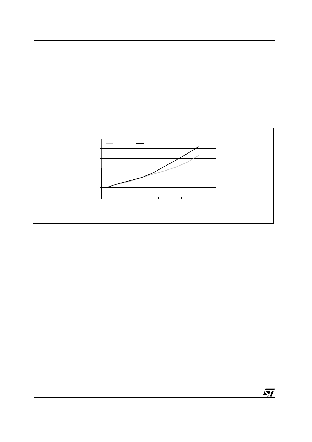
products stands in the law of the on-resistance variation as a func tion of tempe rature. A s c an be seen in
figure 2, the thermal coe fficient is just 1.7 at 125ºC as oppos ed to greater than 2 in conv entional high
voltage MOSFETs. The final result is reduced power dissipation which makes improved system efficiency
whereas the lower gate charge implies using smaller and more economic gate drives.
January 2001
1/8
Page 2
AN1316 - APPLICATION NO TE
2. APPLICATION FIELDS.
The MDmesh™ used in the following applic ation can be used in medium power S MPS application s such
as those encountered in servers and high-end desktops. Other areas such as portable welding
equipment can also benefit from the feat ures of the new device. Advan tages brought to the end user are
maximized when al l system implications a re seen and not just the device itself. Switching losses are
reduced because of lower intrinsic capacitance, shorter crossover t ime and much smaller gate charge
(one-third of that of the conventional devices of similar on-resistance), whereas on-losses are decreased
essentially bec ause of R
DS(on)
.
Figure 2: MDmesh™ R
versus Temperature
DS(on)
3
2.5
2
1.5
1
0.5
0
MDmesh™ Conventional MOSFET
-50 -25 0 25 50 75 100 125 150
Temperature [°C]
3. INTRODUCTION.
The purpose of the following analysis is to compare the electrical and thermal performance of the
STW15NB50 standard MOSFET (500V, 0.36Ohm max, TO-247) with the new MDmesh™ (500V,
0.4Ohm max, TO-220) in a 360W power supply. The STW15NB50 already shows a bet ter on-resistance
than most similar 0.4Ohm industry products with its 0.36Ohm max. So it is expected that any
performance gap between the MDmesh ™ and similar competitors’ devices can be wider than it is in our
case. Also, in this analysis one can see how the new technology opens up new challenging opportunities
to power conversion designers.
In the tests, the two MOSFETs were mounted in positions marke d Q1 and Q2, as shown in figure 3 and
under maximum nominal working operation. Our attention was focused on electrical and thermal
parameters such as V
, Vds, Id, switching characteristics, operating frequency, duty-cycle, switching
gs
energy and steady state heatsink temperature. Based on t he measurement results, some conclusions
were drawn in order to evaluate all performance improvements and energy saving with the new
MDmesh™ technology.
2/8
Page 3
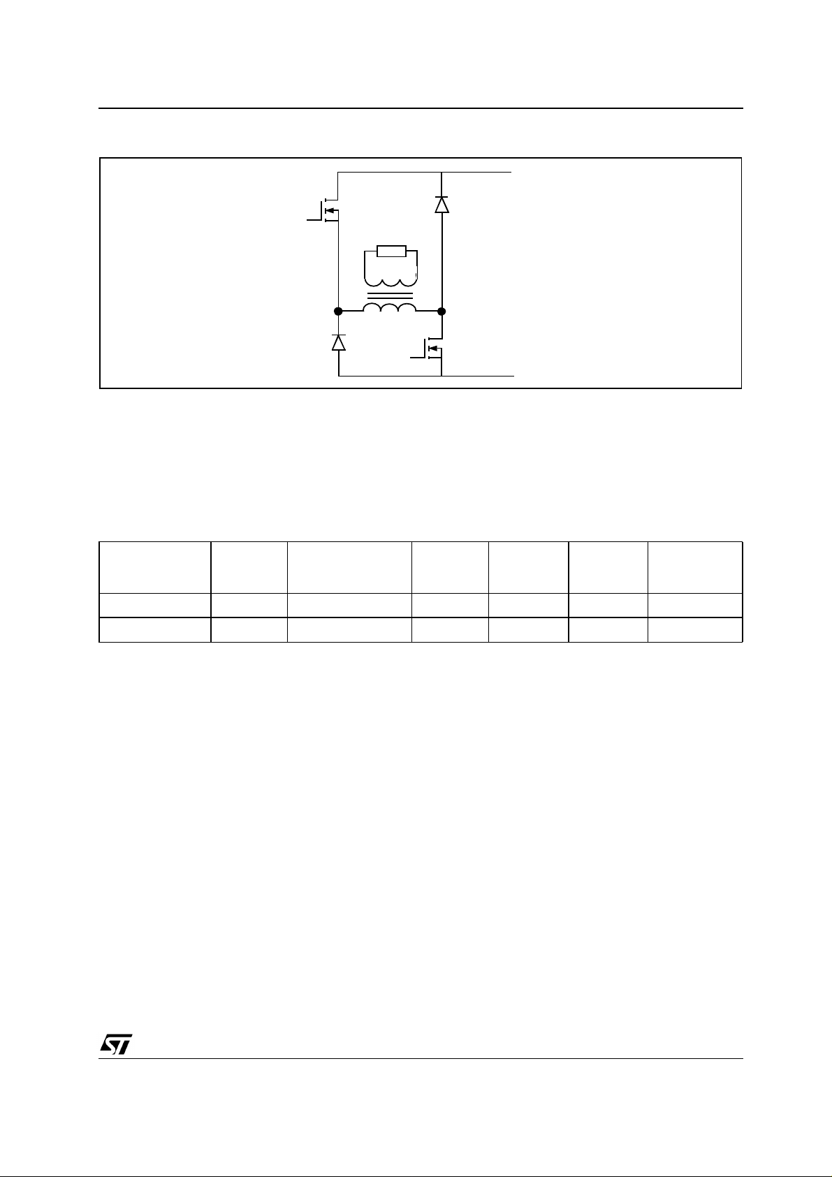
Figure 3: Circuit Configurat i on
AN1316 - APPLICATION NOTE
Vcc
Gnd
Q1
D
D2
S
G
D1
LOAD
Q2
D
G
S
4. STATIC CHARACTERISTICS AND CIRCUIT CONFIGURATION
In the circuit, the devices are connected in an asymmetrical full bridge configuration (figure 3), where the
load is the primary winding of a transformer.
The main static characteristics of the two devices under test are summarized in the below table.
Table 1: Main Electrical Characteristics
V
dss
[V]
R
DS(on)
[Ohm]
@ 25ºC
C
iss
[pF]
C
oss
[pF]
C
rss
[pF]
Package
STW15NB30 >500 0.35 2,600 330 40 TO-247
MDmesh™ >500 0.37 930 160 25 TO-220
5. TEST DESCRIPTION AND OPERATION
The unit was supplied from 220VAC. Then, the +5V output was loa ded with 0.084Ohm and the +12V
output with 3Ohm, so that the total output power was 348W, very close to the max imum nominal o utput
power. The normal operation of Q1 of both MOSF ETs is shown in figure 2 when loaded as mentioned
above.
The duty-cycle and frequency were not constant, as thought, but variabl e due to the voltage ripple from
the PFC section. The duty-cycle ranged between 37% and 43% and the freq uency betw een 110kHz and
120khz.
Figures 4 and 5 show the turn-off of both devices. The MDmesh™, due to its lower capacitance, switched
faster than the STW15NB50 (see table1).
3/8
Page 4

AN1316 - APPLICATION NO TE
Figure 4: MDmesh™ Turn-off
Figure 5: STW15NB50 Turn-off
V
ds
V
gs
I
ds
V
ds
V
gs
I
ds
In figure 6 and figure 7 t he turn-on of both of the M OSFETs is compared and a gain the MDmesh™ is
faster. In fact the gate-to-source voltage, V
, of the MDmesh™ takes about 100ns less to reach its
gs
maximum value (about 12V) compared to the STW15NB50.
Figure 6: MDmesh™ Turn-on
V
ds
V
gs
I
ds
4/8
Page 5

AN1316 - APPLICATION NOTE
Figure 7: STW15NB50 Turn-on
V
ds
V
gs
I
ds
6. TEMPERATURE MEASUREMENTS.
In order to perform a thermal comparison between the MDmesh™ and the STW15NB50 Q1 was
mounted on a 11°C/W heatsink while Q2 was left on its original heatsink. T hen the power supply was
powered and loaded as mentioned before. Under these conditions, the steady state temperature was
measured in a hole made in the heatsink unde rneath the device package. In table 2 the temperature
measurements performed on the devices while the ambient temperature was around 25°C are
summarized.
Table 2: Temperature Measurements
Steady St ate Temperature
STW15NB50 102°C
MDmesh™ 91°C
7. THERMAL CONSIDERATION.
Since the MDmesh™ temperature has bee n fou nd to be 11°C lower than that of the STW15NB50, in the
next step some consideratio n will be done i n order t o high light the reas ons behi nd t he power sav in g and
what is the predominant part (on-state or switching) allowing the MDmesh™ to operate more efficiently
when compared to conventional technologies.
In spite of the voltage and current across them, the power MOSFETs are easily measurable. In this
power supply their fast rate of chang e does not allow us to calculate the averag e power dissipation in
steady state conditions. For this reason the power MOSFETs were mounted on the same heatsink (about
11°C/W of thermal resistance) used for the previous temperature measurement and biased with a DC
voltage, giving the equivalent power needed to reach the same temperature measured in the application.
In such a way the total power dissipation, P
, that in the actual application is the sum of two terms
tot
difficult to determine (switching and conduction), was found by just measuring two equivalent continuous
parameters (current and voltage on the MOSFET).
5/8
Page 6

AN1316 - APPLICATION NO TE
8. TEST RESULTS.
Table 3: Test Results
V
[V]
ds
I
ds
[A]
P
diss
= Vds * I
[W]
ds
R
DS(on)
@ oper. temp
[mOhm]
STW15NB50 2.2 3.17 7 694
MDmesh ™ 1.95 2.98 5.8 653
From the previous test the R
of the devices at their related temperatures were obtained.
DS(on)
Using the results of these measurements we can calculate the power saved by the new MDmesh™
technology compared to the standard one.
Knowing R
for both devices, we can calculate the on-state losses in the application:
DS(on)
P
on
R
DS on()
⋅=
2
I
And since the current is equ al in both devices, we can also calculate t he ratio between the on-state
power losses:
STW15NB50()
P
on
-----------------------------------------------------
P
MDmesh()
on
R
DS on()
----------------------------------------------------------------- -
R
STW15NB50()
DS on()
MDmesh()
1.062==
Basically the last equation proves that in on-state the STW15NB50 dissipates 6.2% more than the
MDmesh™.
Furthermore, from the switching energy measurements we can calculate the ratio between both
switching energies:
P
STW15NB50()
sw
----------------------------------------------------- -
P
MDme sh()
sw
31.3
-----------
22.6
1.384==
Switching losses of the STW15NB50 are also bigger in this case.
We still have extra information from the total power measurements performed with continuous
parameters and more specifically we know:
P
STW15NB50()P
sw
STW15NB50()+ 7W=
sw
and
P
MDmesh()P
sw
MDmesh()+ 5.8W=
sw
Solving the equations (2) trough (5) we can find the values of power loss in both the on-state and
switching condition for both devices and these values are summarized in table 4.
6/8
Page 7

Table 4: Switching and Conduction Losses
AN1316 - APPLICATION NOTE
Switching Losses
[W]
Conduction Losses
[W]
STW15NB50 3.6 3.4
MDmesh™ 2.6 3.2
Now we can calculate the power saving allowed by the new MDmesh™ versus the standard MOSFET.
PS
switching
3.6 2.6– 1W==
and
PS
switching
3.4 3.2– 0.2W==
From the last two equations it turns out that most of the power is saved thanks to the improved switching
characteristics of the new technology, while the conduction offers a big advantage in view of the
difference in die size of the two devices.
The next ste p w ill b e t o estimate the junc t ion tem p er ature based on the R
R
DS(on)
(Tj)=0.653Ohm and R
(25°C)=0.373Ohm are from the measurements performed on the
DS(on)
measurements.
DS(on)
MDmesh™. As the ratio is equal to 1.75, it is possible to read the junction temperature from the
normalized on-resistance versus temperature curve. The junction temperature is about 105°C.
In the same way, knowing R
(Tj)=0.694Ohm and R
DS(on)
(25°C)=0.355Ohm for the STW15NB50 it is
DS(on)
possible to find that its junction temperature is 111°C.
Now the junction temperatures found will be verified to be consistent with the values obtained by using a
different approach. Since the total power loss is known as well as the thermal resistance of the two parts,
keeping in mind that the MDmesh™ package is a TO-220 while the STW15NB50 is housed in TO-247, it
is possible to write:
T
where R
j
, R
th-c-ins
T
heat ksin
th-ins
R
th j–c
, and R
R
+++()+ P
–
th c–ins
th-ins-heatsink
represent the case-to-insulation, insulation layer, and
R
–
th ins
R
–
th ins–heat ksin
–
⋅=
losses
insulation-to-heatsink thermal resistances.
Making the substitution in the last equation for both devices we have the following results:
T
–
j MDmesh
91 1 0.5 0.4 0.5+++()5.8⋅+ 104°C==
and
T
–
j STW15NB50
As seen, these two values are pretty much equal to the ones calculated using the dependence of R
102 0.65 0.24 0.2 0.24+++()+ 7⋅111.3°C==
DS(on)
from temperature.
7/8
Page 8

AN1316 - APPLICATION NO TE
9. CONCLUSION
The main advantage of using the new MD mesh™ techn ology is the remarkable re duction in the power
loss which, in turn, allows a lower operating junction temperature even with smaller packages. A
significant contribution to this power saving is achieved through a drastic improvement in its switching
characteristics. In fact, a smaller die size and, abov e all, the optimized layout realized us ing ST unique
technology, leads to devices with reduced intrinsic capacitances and gate charge. This means that the
device can be operated at higher frequencies. In this case at 115kHz there is a reduced power
consumption of about 28%.
The other contribution to the power saving is the conduction loss. That is, the higher the junction
temperature the more pronounced the overall reduction in on-loss. For instance, with two devices
exhibiting the same R
is possible to have a saving due to the contribution of R
at 25°C, one with standard technology and the other in MDmesh™ version, it
DS(on)
of around 13%.
DS(on)
Information furnished is believed to be accurate and reliable. However, STMicroelectronics assumes no responsibility for
the consequences of use of such information nor for any infringement of patents or other rights of third parties which may
result from its use. No license is granted by implication or otherwise under any patent or patent rights of
STMicroelectro nics. Specification men tioned in this publication are subject to change wit hout notice. This publication
supersedes and replac es all informa tion previ ously supplied. STMicroe lectro nics prod ucts are not autho rized for use as
critical components in life support devices or systems without express written approval of STMicroelectronics.
The ST logo is a registered trademark of STMicroelectronics
© 2001 STMicroelectronics - Printed in Italy - All rights reserved
STMicroelectronics GROUP OF COMPANIES
Australia - Brazil - China - Finland - France - Germany - Hong Kong - India - Italy - Japan - Malaysia - Malta - Morocco -
Singapore - Spain - Sweden - Switzerland - United Kingdom - U.S.A.
http://www.st.com
8/8
 Loading...