

Page 1
AN1301
APPLICATION NOTE
STE100P - SINGLE PORT FAST ETHERNET TRANSCEIVER
1.0 GENERAL DESCRIPTION
The STE100P, also referred to as STEPHY1, is a high perf ormance Fast Ethernet phy si cal l ayer i nt erfac e for
10BASE-T and 100BASE-TX applications. It was designed with advanced CMOS technology to provide a Media
Independent Interface (MII) for easy attachment to 10/100 Media Access Controllers (MAC) and a physical media interface for 100BASE-TX and 10BASE-T. The twist ed pair int erface direct ly drives a 10/100 twisted pai r
connection. STE100P is an excellent device perfectly suited for hub, switch, router and other embedded Ethernet applications.
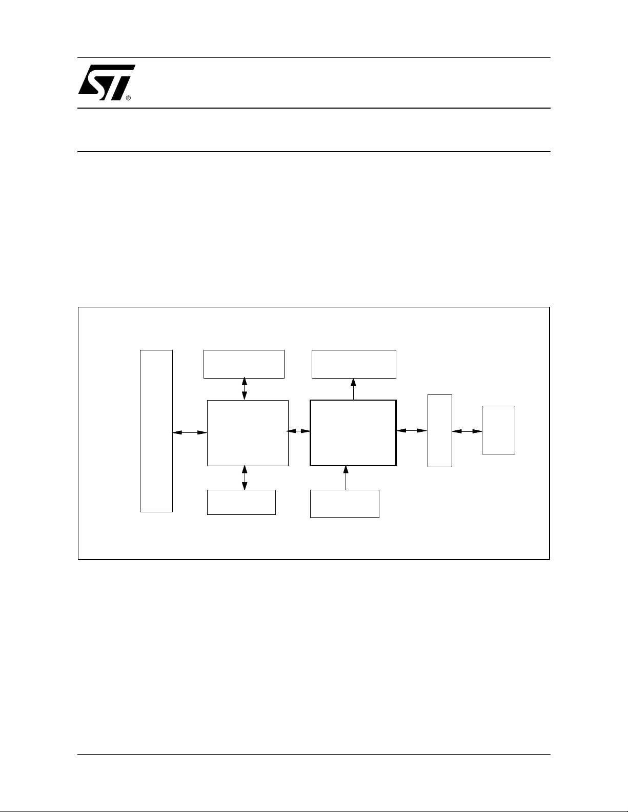
The system diagram is as shown below:
Figure 1. System Diagram of the STE100P Application
Serial
EEPROM
M A C
D ev ic e
PCI Interface
Boot ROM
LEDs
STE100P
STEPHY1
25 MH z
Crystal
RJ-45
Transformer
2.0 FEATURES
n Integrates the whole physical layer functions of the 100BASE-TX and 10BASE-T
n 3.3V low power operation
n The hardware control pins set the initial state of the STE100P at power-up
n Designed with a power down feature, which can save the power consumption significantly
n Can operate for either full duplex or half duplex network applications.
n MI I in terface
n Provides auto-negotiation, parallel detection or manual control for mode setting
n Provides MLT-3 transceiver with DC restoration for Base-line wander compensation
November 2003
1/8
Page 2

AN1301 APPLICATION NOTE
n Provides transmit wave-shaper, receive filters, and adaptive equalizer
n Provides loop-back modes for diagnostic testing
n Builds in Stream Cipher Scrambler/Descrambler and 4B/5B encoder/decoder
n Supports external transmit transformer with turn ratio 1:1
n Supports external receive transformer with turn ratio 1:1
3.0 DESIGN AND LAYOUT GUIDELINES
3.1 General Guidelines
n Verify that all components meet application requirements.
n Design in filters for the analog power circuits.
n Use bulk capacitors (10-22uF) between the power and ground planes t o minimize switching noise, par-
ticularly near high-speed busses (>25 MHz).
n Use an ample supply of 0.1uF decoupling capacitors to reduce high-frequency noise on the power and
ground planes.
n Use a single analog power and ground plane for multiple devices. Keep ferrite bead currents under 65%
of the rated load
n Avoid breaks in the ground plane, especially in areas where it is shielding high-frequency signals.
n Keep power and ground noise levels below 50mV
n Keep high-speed signals out of the area between STE100P and the magnetics
n Ensure that the power supply is rated for the load and that output ripple is minimal (<50mV)
n Route high-speed signals next to a continuous, unbroken ground plane.
n Provide impedance matching on long traces to prevent reflections.
n Do not route any digital signals between the STE100P and the RJ-45 connectors at the edge of the
board
n It is recommended to fill in unused areas of the signal planes with solid copper and attach them with
vias to a Vcc or ground plane that is not located adjacent to the signal layer.
3.2 Differential Signal Layout Guidel ines
n Route differential pairs close together and away from everything else
n Keep both traces of each differential pair as close to the same length as possible.
n Avoid vias and layer changes
n Keep transmit and receive pairs away from each other. Run orthogonally, or separate with a ground
plane layer.
3.3 Power and Ground
In order to obtain high speed communications design, the power and ground planes may be conceptually divided into three regions (the analog and digital power planes and the signal ground plane)
The analog power region extends from the magnetics back to the STE100P, whereas the digital power region
extends from the MII interfaces of t he STE100P through the rest of the board. Only components and signals
pertaining to the particular interface should be placed or routed through each respective region. The digital section supplies power to the digital Vcce/i pin and to the external components. The analog section supplies power
to Vcca pins of the STE100P.
The signal ground region is one continuous, unbroken plane that extends from the magnetics through the rest
2/8
Page 3

AN1301 APPLICATION NOTE
of the board. The signal ground pl ane may be combined wit h chass is ground or i solated f r om it. If the ground
planes are combined, an isolation area is not required. When laying out ground planes, special care must be
taken to avoid creating loop antenna effect. Some guidelines are as follows-
n Run all ground plane as solid square or rectangular regions
n Avoid creating loops with ground planes around other planes
3.4 Recommendations
The following recommendations apply to design and layout of the power and ground planes and w ill p reven t the
most common signal and noise issues.
n Divide the Vcc plane into two sections - analog and digital. The break between the planes should run
under the device.
n When dividing the Vcc plane, it is not necessary to add extra layers to the board. Simply crate moats or
cutout regions in existing layers.
n Place a high-frequency bypass cap (0.1uF) near each analog Vcc pin
n Join the digital and analog sections at one or more points by ferric beads. Ensure that the maximum
current rating of the bead is at least 150% of the nominal current that is expected to flow through it.
(250mA per STE100P)
n Place a bulk capacitor (22uF) on each side of each ferrite bead to stop switching noise from travelling
through the ferrite.
For designs with multiple STE100P’s, it is acceptable to supply all from one analog Vcc plane. This plane can
be joined to the digital Vcc plane at multiple points, with a ferrite bead at each one.
4.0 TWISTED PAIR INTERFACE
4.1 Transmit Interface Circuitry
Figure 2 shows a typical transmit interface circuitry. Current is sourced by the AVddt output to the centertap of
the primary side of the winding. Current flows from the centertap to TX+ and TX-. Other components are as follows:
n R1 and R2 are 49.9 ohm resistors that provide impedance matching to the line, which has a nominal
impedance of 100 ohm.
n C1 shunts any common-mode energy present in the output to ground.
n The magnetics consists of the main winding and a common-mode choke.
n The common-mode choke stops common mode energy from reaching the line. It works together with
capacitor C1 to direct common-mode energy away from the line.
3/8
Page 4

AN1301 APPLICATION NOTE
Figure 2. Transmit Interface Circuitry
4.2 Receive Termination Circuitry
The receive termination circuit as shown in Figure 3 is a simple 100 ohm, 1% resistor across the RX+/
RX- pair. The receive circuit consists of magnetics, which include a main winding and a common-mode
choke, and termination resistance to match the line impedance. The common-mode chok e can be
located on either the primary or secondary side of the winding. Some vendors place the receive common-mode choke on the line-side (primary) of the main winding while others place it on the device side
(secondary). Either location is acceptable.
Figure 3. Receive Interface Circuitry
4/8
Page 5

AN1301 APPLICATION NOTE
4.3 Standard termination
ST recommends a standard termination for the unused pairs on the twisted-pair interface as shown in
Figure 4. The termination basically looks like a 100 ohm load, matched to the line, which is by passed to
chassis ground. This termination is added for robustness and noise reduction.
Figure 4. Sugg es te d Term i nat i on Circ u it
5.0 CRYSTAL REQUIREMENTS
The crystal to be used with the STE101P should be a 25 MHz fundamental mode crystal operating in parallel resonance, connected as shown in the sample application circuit schematic (see section 7.1). The
following table shows the specifications for the crystal:
Parameter Units Min Max Nom
Frequency MHz - - 25.0
Frequency Stability ppm - +
Load Capacitance pF 18
Shunt Capacitance pF 8
50 -
Table 1
5/8
Page 6

AN1301 APPLICATION NOTE
6.0 LED PINS
The LED display, consists of five LEDs having the following characteristics:
n Speed LED: 100Mbps(on) or 10Mbps(off)
n Transmit/Receive LED: Blinks at 10Hz when transmitting or receiving, but not colliding
n 10Mbps LED: Blinks at 10Hz when transmitting, but not colliding
n Link LED: On when 100M or 10M link ok
n Collision/FD LED: Blinks at 20 Hz to in dicate a collis io n. On to indica t e full dup le x op er ati o n
7.0 TYPICAL APPLICATION
While the STE100P may be used in a variety of applications such as multi-port repeaters or switches, the
application shown below gives a very simple way of evaluating and using the STE100P with minimum circuitry. (Refer to Bill of Mat e r ials in Table 2)
A typical application of the STE100P presented here would be in designing a Fast Ethernet transceiver
with a standard MII interface and a 10/100 Mbps twisted pair connector. (Refer to Fig. 5)
In this application,
n STE100P is the only IC needed.
n It connects directly to the industry standard 40-pin MII connector.
n It also connects to the RJ-45 jack via a standard Fast Ethernet transformer.
n 5, 4-position DIP switches are used to select the PHY address. (More details on the PHY address reg-
isters, etc. are available on the STE100P datasheet)
n 2, 10-position DIP switches are used for determination of all of the pin-selectable options of the
STE100P such as duplex mode, data rate and auto negotiation.
n STE100P also supports the MII MDIO access to all of its internal registers.
n LEDs are included to indicate status information such as speed, duplex mode, transmit and receive ac-
tivity and link status.
n There are registers with 16 bits each supported for STE100P. (More details on these registers are avail-
able in the STE100P datasheet).
n There are also 4 special registers for advanced chip control and status information.
7.1 Schematics
The schematics for the sample application can be found on the the following page and the ST website at:
http://www.st. com/prodpres/dedicate/telecom/network/datacom/st100p.htm
6/8
Page 7

AN1301 APPLICATION NOTE
4
3
2
1
VDD
C51
22UF
C52
22UF
of
11Thursday, October 26, 2000
In
E
V3.3T
L2
BEAD
C2
0.1UF
AVddT
Don't stuff L3 if both U4 & U6 are used.
L3
BEAD
D
AGND
V3.3
L1
BEAD
C1
0.1UF
VCCA
AGND
AVddT
C
LEDTR
LED10
LEDL
GND
GND
1
CRS
crs
2
COL
col
3
TXD<3>
txd3
4
TXD<2>
txd2
5
TXD<1>
txd1
6
TXD<0>
txd0
7
TX_EN
tx_en
8
TX_CLK
tx_clk
9
TX_ER
tx_er
10
RX_ER
rx_er
11
RX_CLK
rx_clk
12
RX_DV
B
U5
MIITest
RXD<0>
RXD<1>
RXD<2>
RXD<3>
MDC
MDIO
+5V
rx_dv
13
rxd0
14
rxd 1
15
rxd2
16
rxd 3
17
mdc
18
mdio
19
20
LEDC
mdio
mdc
rxd3
rxd 2
rxd 1
rxd0
rx_dv
LEDS
V3.3
crs
col
AGND
C61
C55
C54
txd3
C6
R1
R2
C5
GND
33
34
35
36
37
38
39
40
41
42
43
44
45
46
47
48
txd2
J1
1234567
R3
10PF
49.9
49.9
10PF
0.1uF
0.1uF
0.1uF
txd0
txd1
1234567
8
RJ45
8
R5
49.9
R4
49.9
10
11
141516
CT
CT
TX-
RX+
TX+
U3
TD+CTTD-
RD+CTRD- RX-
12367
8 9
TP13
0
1
C8
TP12
C7
0.1UF
1
R6
AGND
PWRDWN
TX-
TP1
1
RIP
TX+
RESET
32
ripncnc
leds
ledc
ledl
ledtr
vcce
mdc
rxd3
rxd2
rxd1
rxd0
gnde
mdio
vcce/i
rx_dv
nc
ledr10
rx_clk
scan_en
gnde/i
rx_er/rxd4
reset
tx_er/txd4
tx_clk
txp
txn
test
vcca
gnda
gnde
pwrdwn
U2
STFEPHY
tx_en
txd0
txd1
txd2
txd3
col
crs
495051525354555657585960616263
MDINT
col
crs
tx_clk
txd1
txd0
txd3
txd2rxd2
tx_en
tx_er
rx_clk
tx_er rx_er
rx_er
rxd1
rx_dv
mdio
rx_clk
rxd3
mdc
rxd0
tx_en
tx_clk
HB626-1
0.1UF
100
RX+
rxp
gnda
fds/mdint
vcce/i
R9
R8
R7
RX-
CFG1
49.9
C11
0.1UF
C9
0.001UF
GND
75
C10
75
0.1UF
CHASSIS
R366
TP8
1
R365
TP15
1
AGND
R364
R363
R362
R361
TP14
1
VCCA
GND
C59
0.1uF
C58
0.1uF
C57
0.1uF
C56
0.1uF
171819202122232425262728293031
rxn
vcca
vcca
R12
4.99K
16
iref
gnda
vcca
x1
x2
gnda
vcca
gnda
gnde/i
fde
mf0
mf1
mf2
mf3
mf4
cfg1
cfg0
64
AGND
15
14
13
12
11
10
9
8
GND
7
6
5
4
3
2
1
MF4
FDE
MF2
MF1
MF3
MF0
CFG0
R14
10k
10k
R11
R10
10k
VDD
C4
22UF
A
C3
20
+5V
COL
CRS
22UF
TXD<3>
GND
GND
GND
+5V
U1
40
TXD<1>
TXD<2>
GND
GND
TX_EN
TXD<0>
GND
GND
TX_ER
TX_CLK
GND
GND
RX_ER
GND
RX_CLK
GND
RX_DV
GND
RXD<1>
RXD<0>
GND
GND
RXD<3>
RXD<2>
GND
GND
12345678910111213141516171819
+5V
MDC
MDIO
MII
+5V
GND
GND
21222324252627282930313233343536373839
R31
R27
10k
10k
R26
10k
GND
U4
Out
C50
V3.3
TP11
1
AGND
0
0
0
0
0
0
C12
R15
X1
MF0
MF1
1819201716
SW9
123456789
R17
10k
10k
R13
CFG0
CFG1
1819201716
SW8
123456789
10k
R23
10k
R30
GND
22UF
GND
22PF
X1
0
MF2
151413121110
R16
10k
PWRDWN
151413121110
10k
R22
GND
In
GND
GND
Out
U6
3.3VReg-L4931CZ33
3.3VReg-L4931CZ33
C53
22UF
V3.3T VDD
1310 Electronics Drive
Mail Station 764
STMicroelectronics, Inc.
340
R371
SW7
5
6
7
8
R36
240
R41
340
R370
SW6
5
6
7
C13
25MHz
22PF
8
R35
240
R40
X2
Notes:
MF3
MF4
340
R369
SW5
5
6
- X 1 is suggested to be 25Mhz +/-50ppm, with
C L = 18pF, and 8pF max shunt capacitance
7
8
R34
240
R39
340
R368
SW4
5
6
7
R21
10k
10k
R25
R20
10k
FDE
RESET
R29
10k
R19
10k
R28
10k
8
R24
10k
GND
R33
240
R38
340
VDD
R367
SW3
5
6
7
8
R18
0 ohm
R32
240
GND
R37
E
STFEPHY1 <00>
Fast Ethernet Single PHY Evaluation Board
B
Carrollton, TX 75006-5039
Title
Size Document Number Rev
Date: Sheet
SW DIP-4
91
R360
D
4
3
2
1
D5
LED
1.1K
LEDC LEDS
SW DIP-4
91
R350
4
3
2
1
D4
LED
C
1.1K
SW DIP-4
91
R340
4
3
2
1
D3
LED
1.1K
B
LEDTR LEDL
SW DIP-4
91
R330
4
3
2
1
D2
LED
1.1K
LED10
R320
SW DIP-4
91
4
3
A
2
1
D1
LED
1.1k
7/8
Page 8

AN1301 APPLICATION NOTE
7.2 Bill of Materials
Following are the Bill of Materials for the STE100P sample application.
Item Qty Refere nce Par t
_______ ___ ___ _____ ___ __ ___ ___ __ ___ ___ __ ___ ___ __ ______ __ ___ ___ __ ___
1 13 C1,C2, C7, C8 ,C10,C 11 ,C5 4, 0.1uF
C55,C5 6,C 57 ,C5 8,C 59 ,C6 1
2 6 C3,C4, C50 ,C 51,C52 ,C 53 22UF
3 2 C5,C6 10PF
4 1 C9 0.001UF
5 2 C12,C1 3 22PF
6 5 D1,D2,D3, D4 ,D5 LED
7 1 J1 RJ45
8 3 L1,L2,L3 BEAD (do no t ins tal l L3
if U4 & U6 both installed)
9 5 R1,R2,R4, R5 ,R9 49.9
10 8 R3,R15,R3 61 ,R362, R3 63, 0 ohm
R364,R 365,R 366
11 1 R6 100 ohms
12 2 R8,R7 75 ohms
13 19 R10,R11,R 13 ,R14,R 16 ,R17, 10k
R19,R2 0,R21 ,R2 2,R23 ,R2 4,
R25,R2 6,R27 ,R2 8,R29 ,R3 0,
R31
14 1 R12 4.99K
15 1 R18 0 ohm
16 5 R32,R33,R 34 ,R35,R 36 240 ohms
17 5 R37,R38,R 39 ,R40,R 41 1.1K
18 5 R320,R330 ,R 340,R3 50 ,R360 91 ohms
19 5 R367,R368 ,R 369,R3 70 ,R371 340 ohms
20 5 SW3,SW4,S W5 ,SW6,S W7 DI P Swi tch DIP- 4
21 2 SW8,SW9 SW DIP-10
22 7 TP1,TP8,T P1 1,TP12 ,T P13, Tes t Pin s
TP14,T P15
23 1 U1 MII 40 pin connector
24 1 U2 STEPHY STE100P
25 1 U3 HB626-1 Transformer
26 2 U4,U6 3.3VReg-L4931CZ33
27 1 U5 MIITest header
28 1 X1 25MHz crystal
Information furnished is believed to be accurate and reliable. However, STMicroelectronics assumes no responsibility for the consequences
of use of such information nor for any infringement of patents or other rights of third parties which may result from its use. No license is granted
by implic ation or otherwise under any patent or patent r i ght s of STMi croelectr oni cs. Specifications menti oned in thi s publicati on are subject
to change without notice. This publication supersedes and replaces all information previously supplied. STMicroelectronics products are not
authorized for use as cri tical components in li f e support dev i ces or systems without express writ t en approval of STMicroel ectronics.
The ST logo is a registered trademark of STMicroelectronics
2001 STMicroelectroni cs - All Righ ts Reserved
Australi a - Brazil - China - Finland - Fr ance - Germany - Hong Kong - India - Italy - Japan - Malaysia - Malta - Morocco - Sin gapore - Spai n
STMicroelectronics GROUP OF COMPANIES
- Sweden - Sw i tzerland - United Kin gdom - U.S.A .
http://www.s t. com
8/8
 Loading...