

Page 1
AN1300
APPLICATION NOTE
L6598 BASED 12V/3A RESONANT APPLICATION
by Eric Danstrom
Off-line switching power supplies have two major problems: high switching losses, and an operating environment, which is very sensitive to the radiation of Electromagnetic Interference (EMI) and Radio Frequency Interference (RFI). The switching losses are a largest creator of EMI (conducted) and RFI
(radiated), sotheir control and reduction isamajor benefit to the power supplydesigner. Resonanttechniques offer a hope for greatly reducing the switching losses and hence the factors contributing to the
EMI and RFI. This paper will present and organized approach to the design of a 36-watt, full-resonant,
off-line converter that can be used for portable PC applications.
Operation of the Resonant Converters
Full-resonant converters are based upon the half-bridge and full-bridge PWM topologies. They are driven with
a symmetrical w aveformwhose frequency is changed to control the output voltage. There is a deadtime provided between the conduction of the upper and lower power switches to turn-on with zero voltage witching. Here
the drain voltage of the MOSFET turning off immediately swings to the opposite voltage and causes the opposing antiparallel diode to conduct The opposing MOSFET can then turn-on with a very low drain-to-source voltage.
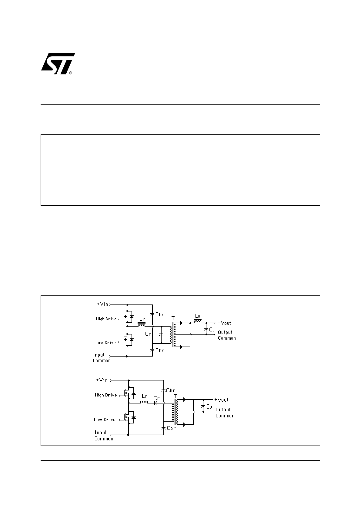
There are two major types of resonant converters: the parallel- resonant converter shown in figure 1a, and the
series-resonant converter shown in figure 1b.
Figure 1. The Two Types of Resonant Converters
October 2000
(a) Parallel
(b) Series
1/9
Page 2

AN1300 APPLICATION NOTE
In the parallel-resonant converter, the load is placed in parallel with the resonant tank capacitor. This is done
through a forward-mode transformer where the output rectifiers conduct simultaneously with the positive and
negative excursions of voltage on the primary winding. The load though, must represent as high an impedance
as possible so it does not load the tank capacitor too much which would excessively lower the tank circuit's "Q".
This is done by the use of a choke-input (L-C) filter following the output rectifiers. The choke input filter is high
impedance when viewed above its filter pole frequency. The output voltage is mathematically the area under
the curve of the output voltage waveform. The number of turns in the secondary winding is therefore higher
than in a series resonant converter.
In the series resonant converter, which is proposed here, the load is placed in series with the resonant inductance and capacitance. Here the load must be low impedance. This is best done by the use of a capacitor-input
filter on the transformer's secondary, where the tank views the low impedance of the output capacitor(s) reflected to the primary winding of the transformer.
Bothresonanttopologies are driven with a symmetrical waveformabovethat tank circuit's resonance frequency.
The output power is controlled by where on the tank circuit's gain Vs frequency curve the converter is operating.
The closer, to the tank's resonance, the higher is the output power.
The series-resonant half-bridge causes the current to resonate in sinusoidal fashion when the tank circuit's voltage is excited at its resonance frequency. The tank circuit is made-up primarily of the resonant inductor (L
the Capacitor (C
), but also incorporates the transformer parasitic elements which also include to varying de-
r
grees, the primary and secondary leakage inductances and the inter-turn and inter winding capacitances. The
load impedance on the secondary of the transformer is also reflected to the primary circuit and becomes a portion of the tank circuit. By incorporating these parasitic elements into the tank circuit, the noise typically generated by their unpredictable behavior within PWM converters is harnessed for real work by the converter.
The half-bridge capacitors (C1, C2) are in series with the tank circuit. Traditionally these are high enough in value such that the center node stays at a fixed voltage of approximately one-half the DC input voltage. These capacitors though could be reduced in value and used as the resonant capacitor itself, thus eliminating the
resonant capacitor. Going yet another step further, these capacitors are electrically in parallel within the resonant circuit, and one of them can be eliminated with no detriment to the converter's operation. The upper capacitor would be the logical choice to eliminate from a reliability standpoint.
The external resonant inductor can also be eliminated, if one realizes that the leakage inductance is in series
with the primary winding, as is the external resonant capacitor. If one purposely makes a transformer with high
primary leakage inductance,one can then eliminate the external resonant inductor in some cases. For the power systems (220-240 VAC), where the transformer has more turns on the primary winding, developing a leakage
inductance of around 100
µ
H is possible. This is done by using a 2-sectioned bobbin where the primary winding
is placed in one-half of the bobbin and the secondary in the other half. This lowering of the coupling between
the primary and secondary and the core, raises the leakage inductance. For the low voltage AC power systems
(100 - 120 VAC), it can be more difficult to create the large leakage inductance, so an external inductor may still
need to be placed within the tank circuit.
The tank circuit's approximate resonance frequency, neglecting the dead time period, can then be then calculated by:
) and
r
f
------------------------------ -=
o
2π L'rC'r
1
[Eq. 1]
Where: Lord is the series combination of Lelk + Lr(ext) if used
C'r is the AC value of the bridge capacitor(s)
This frequency will be the primary point of reference for the converter. The control circuit must always stay
above this point to maintain the advantage of zero current switching in the semiconductors.
The output load determines the "Q" of the power stage. Its equivalent resistance is reflected through the trans-
former. This is given by equation 2.
L
r
----- -
C
2/9
---------------------------- -=
Q
R
r
+
priRrefl
[Eq. 2]
Page 3
AN1300 APPLICATION NOTE
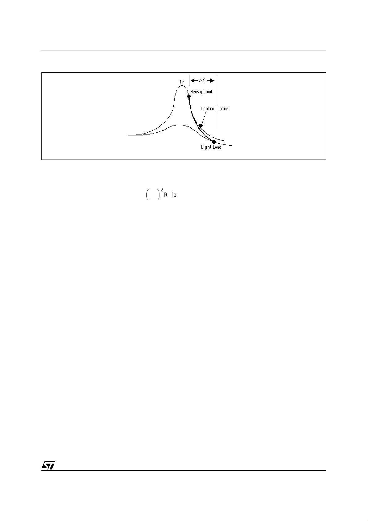
Figure 2. The Control-Transfer Function of the Series-Resonant Converter
The damping resistance is the sum of the resistances within the primary circuits and the reflected load resistance. The equivalent resistance is reflected through the transformer. This is given by equation 3.
2
N1
R
refl
The typical transfer function of the resonant current within the tank circuit is shown in figure 2. It shows when
the converter provides more output power by lowering its frequency. The amplitude of the current grows significantly. Conversely, whenthe load lightens, the control loop increases the frequency away from the tank circuit's
resonance. Simultaneously, the Q of the tank circuit decreases slightly.
Figure 3 shows the converter operating at 110% of rated load and the operating frequency is permitted to go
under the resonant frequency of the tank. This condition may occur when the input voltage is at its minimum
rating and the output is at rated or slightly over-rated load and the frequency lower limit is not set properly.
Period 1 is the deadtime of the power switches when the center node voltage between the MOSFETs swings
from one voltage rail to the opposite rail. After the voltage has transitioned, the primary current flows through
the opposing MOSFET’s antiparallel diode.
The rate of change in the voltage waveform is dictated by the sum of the parasitic capacitances on the node.
These would be primarily the output capacitances of the MOSFETs.
Period 2 begins when the opposing MOSFET turns-on. Current is already flowing through the antiparallel diode
when the MOSFET turns ON. The current will continue its decline driven by the tank circuit and then reverse
direction. During periods 1 and 2, the secondary voltage on the forwardwinding transitions to the output voltage
and the winding’s current begins a sinusoid-like increase. the peak and decline again towards zero where another deadtime is encoundered and the period repeats in the opposing direction.
When the input voltage is low and the output power draw is at or greater than its rated putput, one begins to
notice a current valley begin to appear just past the peaks of the primary current. The supply may be operating
below resonance. This "inflection" in the primary current waveform increases as the input voltage is further lowered or the output load is increased.
Waveforms at light load can be seen in figure 4. Here, the two normal operating periods (1 & 2) are seen.
------- -
N2
R load()=
[Eq. 3]
3/9
Page 4

AN1300 APPLICATION NOTE
Figure 3. The Waveforms of a Series-Resonant Supply slightly Overloaded.
Figure 4. The Primary Waveforms of the Series-Resonant Supply at Light Load.
4/9
Page 5

AN1300 APPLICATION NOTE
DESIGNING 36 WATT SERIES RESONANT CONVERTER
General Specifications:
Input Voltage: 85 - 130 Vrms
Output Voltage: 12 VDC +/- 2%
Rated Output Current: 3 A
Lightest Output Current: 0.5 A
The tank circuit will operate at a resonant frequency of 100 kHz.
Transformer Design
TheE-Ecore size for a forward converterof this output power isabout 25 mm. Iwill use TDK part number EE25/
19 core using the H7C1 material in this example.
The number of turns needed for the primary, operating at about 40 percent of the saturation flux density (1800
G), is about 49 turns. We will use a 2 section bobbin to "enhance" the primary’s leakage inductance, though, is
a very complex phenomenon, and this result will only be a rough estimation.
2
l
ins
b
w
------ -+
3
[Eq. 4]
L
leak
K1 Lmt()nx
------------------------------- - T
≈
100W
Where:
K1 is equal to 3 for a simple primary and secondary winding
L
is the mean length of a turn around the bobbin for the whole winding (in).
mt
is the turns contained in the winding being analyzed
n
x
W1 is the length of the winding from end-to-end (in)
T
is the thickness of the wire insulation (in)
ins
b
is the build (or thickness fromthe bobbin center-leg) of all the windings of the completedtransformer (in)
w
This relationship shows the largest factors in the amount of leakage inductance a winding will exhibit, is most
influenced by the length of the winding (W
), the turns (nx) and the number of layers of turns (bw).
l
Plugging in the wire and core-related dimensions and solving, one arrives at a preliminary leakage inductance
of 44
µ
H. This will be used to calculate a preliminary value for the resonant capacitor.
The number of turns needed for the auxiliary and output windings will be 10 turns. I will use litz wire on the
secondary winding of 12 strands of 30 AWG to enhance the flexibility of the wire.
Design of the Tank Circuit
Calculating the value of the resonant capacitor to produce a resonance frequency of 100 kHz, one uses:
1
------------------------ -=
C
r
2
L
2πrf()
r
Solving for this, using the leakage inductance found above, one gets a resonant capacitance of 0.056
[Eq. 5]
µ
F.
Design of the Output Circuit
The value of the output capacitance to produce the desired level of ripple voltage is found by:
I
out max()
---------------------------------------- -=
C
o
()
fV
This makes the output capacitance equal to 100
1d–[]
[Eq. 6]
ripp le p p–()
µ
F, which is needed to produce a ripple voltage of 30 mV when
the power supply is fully loaded at an output of 3 amperes.
5/9
Page 6

AN1300 APPLICATION NOTE
Design of the Input Circuit
The input filter capacitor’s value is determined by the amount of ripple one desires on the DC input voltage of
the converter. The ripple voltage of 5-10V is typical. The input capacitor can then be estimated by:
0.3P
C
in()
--------------------------------------------------------------------- -≈
finV
()V
in min()
The approximate value of the input capacitor is then 100-150
The 60Hz input rectifiers for the typical capacitor input filter would be determined by the current that is higher
than the average input current but lower than the estimated peak current. The input current rating is then approximated by Eq. 8.
P
in rated()
I
in rect()
----------------------------- -≈
0.4V
The input current rating of the input rectifier should then be equal to or greater than 0.8A. The reverse voltage
rating would then be 2 times the peak input voltage or 400V. The input rectifiers should then br 1N4004.
Selection of the Semiconductors
The power Switches:
Since this is a half-bridge 155 VAC application, the power MOS FETs need only have a breakdown voltage
(V
) of between 200 to 250 volts. The choice of N-channel MOSFET is the IRF630S.
DSS
in()
()
ripple p p–()
µ
F
in min()
[Eq. 7]
[Eq. 8}
The output Rectifiers:
The minimum reverse voltage that the output rectifiers will see will be about 25 volts. The RMS current that
each output rectifier will see will be about 1.5 amperes. The diode current waveform will be a half-rectified sine,
whichwill have an approximate peakvalue of 6 amperes. Since its peak current is muchgreater than its average
current, it is a good idea to select a schottky rectifier that is about thevalue of thepeakvalue, to keepthe voltage
drop during the conduction time to a minimum. Therefore a rectifier of 5 or more amperes would wise. A good
choice would be STPS8L30B. This rectifier is an 8 A schottky diode with a reverse voltage of 30 V.
Design of the Control Circuitry:
The functions that need setting-up are the excursion limits of the frequency control. These are controlled by the
4pins; R
fmin,Rfstart,Css
and Cf. The frequency parameters of these pins must be referenced to the resonant
frequency of the tank circuit. Some adjustment will be necessary after the converter is built, to set the control
loopto the actual resulting resonance frequency of thephysical tank circuit. In a production setting, these control
limits should be checked with the production transformer and resonant capacitor.
There is some interaction between the frequency-setting pins. This is necessary for consistent operation of the
VCO.
The soft-start capacitor is determined by:
SS
------------------------------------ -=
T
SS
C
0.15 /µFsec()
For a 0.5 second soft-start period the soft-start capacitor is approximately 0.3
One then determines the minimum operating frequency, which should be set at approximately 1.1f
is one equation and two unknowsns. I will select theoscillator capacitor as 360pF. The R
1.41
R
fmin
---------------------=
()
f
minCf
[Eq. 9]
[Eq. 10]
µ
F.
. Since there
r
resistor is found by:
fmin
Rfmin is then approximately 36k
6/9
Ω.
Page 7

AN1300 APPLICATION NOTE
From a graph, the value o f R
should use a 33k
Ω
resistor on pin 2.
to produce a +80kHz start frequency or a start frequency of 190KHz, one
fstart
Design of the Bootstrap Start-up Circuit
The bootstrap start-up circuit is intended to allow a small amount of current from the input voltage tothe control
IC when power is first applied. It is also intended to restart the converter in the event of an output overcurrent
situation. The selected circuit allows a current of about 1mA to charge the IC bypass capacitor should have
enoughstored energy to start the converter, after which IC can then be powered directly from the auxiliarywinding on the power transformer. The input start-up current is not high enough to allow sustained operation of the
ICandMOSFETdrive. This results in a "hiccup" overcurrent start-up. Another nice operational mode is the input
start-up current is turned off after the converter has started thus saving several watts of power during operation.
The selection of the small signal NPN transistor for the 115V AC line should hinge mainly upon thr V
device. For higher voltage AC lines, the P
and arc-over voltage of the package become more of an issue. The
D
CEO
of the
transistor that meets the needs of the converter is the SO642.
The start-up resistor (collector Resistor)
R(start) is found by:
120V 12V–()
R
start
------------------------------------ 108k or 100k==
1mA
The base-bias resistor R(bias) must supply both the base current and the minimum amount of current needed
to operate the zener diode (225mW) at its "knee" voltage:
R
bias
120V 12V–()
--------------------------------------- - 379 k==
250µA
I
c
--------- -+
h
FE
Make this resistor 360k.
Compensating the feedback Loop:
The bandwidth of the control circuit is being set to 15kHz which produces a very good response time for almost
all switching power supplies.
The resonance frequency of the tank circuit presents a peculiar set of problems for stability. Approaching the
resonancepoint from below, the gaindrastically incresesand the gain begins todecrease. Above the resonance
frequency, both the gain and the phase are frequency, both the gain and the phase a re decreasing rapidly.
Since the resonance point of the tank circuit and the ESR of the output capacitor are not fixed, it is advisable to
roll-off its gain below to the tank circuit’s resonance frequency. One can do this by calculating the gain of the
open-loop circuit at DC. The gain is essentially the minimum input voltage divided by the change needed in the
control voltage (2V) which produces a +35.5dB gain at DC. By closing the loop, one must have an attenuation
of 35.5dB at 15kHz to produce the desired closed-loop gain and phase. There are of course other methods of
closing the loop with mixed results. This is the most conservative, thus yelding a guaranteed stable system.
To set the frequency of the crossover frequency of the error amplifier one, essentially "substracts" the DC gain
of the control-to-output" characteristic or:
35dB– 10Log
=
ep
-------
f
xo
[Eq. 11]
f
using a15kHz closed loop bandwidth and solving, resultsin an error amplifier bandwidth of 252Hz.Thensolving
the equation;
C
f
This yields a feedback capacitor of 0.066
1
------------------- -=
2πRf
µ
F
ep
[Eq. 12]
The final schematic is shown in figure 5.
7/9
Page 8

AN1300 APPLICATION NOTE
Figure 5. The 36W, Off-line Series-Resonant Converter
Vin(D C)
47uF
+
47uF
250V
250V
R5
100K
Voltage
Doubler
+
120k
½W
220V
N
110V
1N4004's
120k
½W
R1
Summary:
At the production prototype stage, the resonant frequency of the tank circuit should be checked over a reasonablepopolutation of transformers and resonant capacitors. the final transformer in this unit had a leakageinductance of 72mH (as opposed to 45 as calculated). A minor adjustment to the value of the resonant capacitor was
required.
The leakage inductance can be held within a fairly tight range, if the transformer manufacturer uses an automated
winding process. This should be discussedwith the perspective transformer manufactures prior to production.
The final efficiency was found to be between 78% at light loads (0.5A) to 91% at rated load (3A).
This type of converter would be the best choice for consumer appliances where the load presented to the con-
verter is fairly constant and where environment is sensitive to EMI.
References:
"L6598", STMicroelectronics Datasheet.
Bildgen, M., "Resonant Converter Topologies", STMicroelectronics Application Notes AN658 & AN1194, 1999.
Brown Marty, "Power Supply Cookbook", Butterworth Heinemann, 1994.
Donahue, Joel, Jovanovic’, Milan, "The LCC Inverter as a Cold Cathode Flourescent Lamp Driver", APEC, 1994.
8/9
Page 9

AN1300 APPLICATION NOTE
Information furnished is believed to be accurate and reliable. However, STMicroelectronics assume s no responsibility for the consequences
of useofsuchinformation nor for any infringement of patents or other rights of third parties which may result from its use. No license is granted
by implication or otherwise under any patent or patent rights of STMicroelectronics. Specifications mentioned in this publication are subject
to change without notice. This publication supersedes and replaces all information previously supplied. STMicroelectronics products are not
authorized for use as critical components in life support devices or systems without express written approval of STMicroelectronics.
The ST logo is a registered trademark of STMicroelectronics
2000 STMicroelectronics - All Rights Reserved
Australia - Brazil - China - Finland - France - Germany - Hong Kong - India - Italy - Japan - Malaysia - Malta - Morocco - Singapore - Spain
STMicroelectronics GROUP OF COMPANIES
- Sweden - Switzerland - United Kingdom - U.S.A.
http://www.st.com
9/9
 Loading...