

Page 1
V
A Li-Ion BATTERY CHARGER USING TSM102A
This application note explains how to use the
TSM102 in an S MPS-type battery charger wh ich
features :
❑ Voltage Control
❑ Current Control
❑ Low Battery Detection and E nd Of Charg
Detection
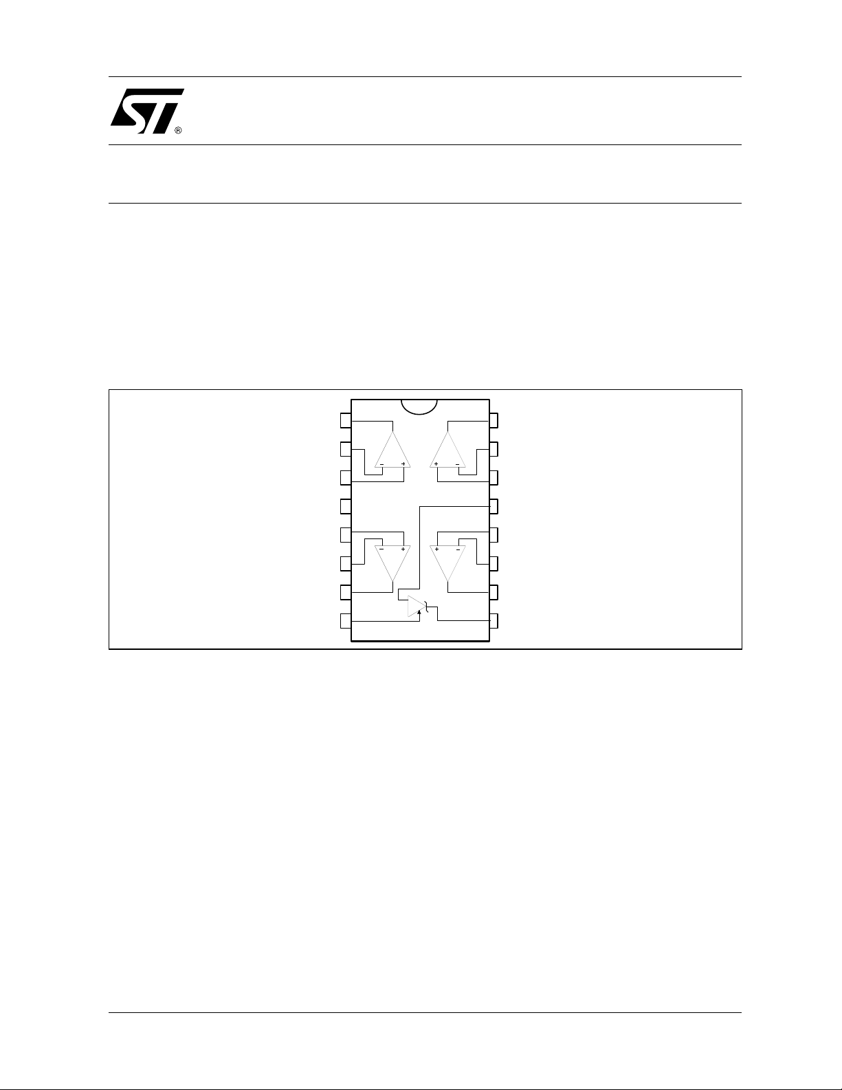
Figure 1 : TSM102 Pinout
AN1284
APPLICATION NOTE
by R. LIOU
1 - TSM102 PRESENTATION
The TSM102 integrated circuit includes two Operational Amplifiers, two Comparators and one adjustable precision Voltage Reference (2.5V to
36V, 0.4% or 1%).
TSM102 can sustain up to 36V power supply voltage.
1
2
3
+
CC
5
6
7
Vref
2 - APPLICATION CONTEXT AND PRINCIPLE
OF OPERATION
In the battery charging field which requires ever increasing performances in more and more reduced
space, the TSM102A provides an attractive solution in terms of PCB area saving, precision and
versatility.
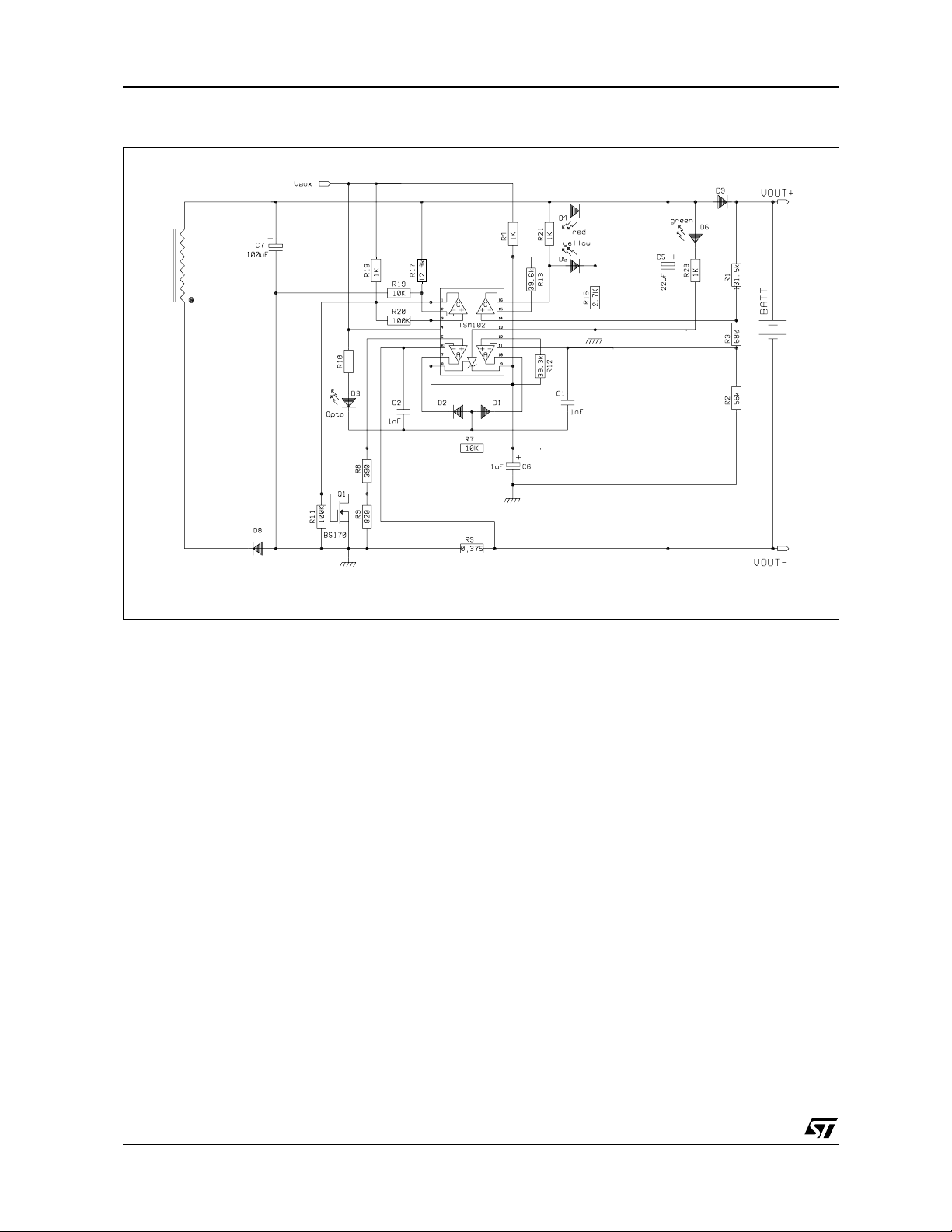
Figure 2 shows the secondary side of a battery
charger (SMPS type) where TSM 102A is used in
optimised conditions : the two Operational Amplifiers perform current a nd voltage control, the two
Comparators provide “End of Charge” and “Low
Battery” signals and the Voltage Reference ensures precise reference for all measurements.
The TSM102A is supplied by an auxiliary power
supply (forward configuration - D7) regulated by a
bipolar transistor and a zener diode on its base
(Q2 and DZ), and s moothed by the capacitors C3
and C4. R15 polarizes the base of the transistor
and at the same time limits the current through the
July 2000
COMP
TSM102
COMP
zener diode during regulation mode of the auxiliary power supply.
The current and voltage regulations are made
thanks to the two Operational Amplifiers.
The first amplifier senses the current flow through
the sense resistor Rs and compares it wit h a part
of the reference voltage (resistor bridge R7, R8,
R9). The second amplifier compares the reference
voltage with a part of t he charger’s output (resistor
bridge R1, R2, R3).
When either of these two operational amplifiers
tends to lower its ouput, this linear information is
propagated towards the primary side via two ORing diodes (D1, D2) and an optocoupler (D3). The
compensation loops o f these regulation functions
are ensured by the capacitors C1 and C2.
16
15
14
V
-
CC
12
11
10
Cathode
1/3
Page 2
AN1284 - APPLICATION NOTE
Figure 2 : The Application Schematic - Battery Charger Secondary Side
The first comparator ensures the “Low Battery”
signal generation thanks to the comparison of a
part of the charger’s output voltage (resistor
bridge R17, R19) and the reference voltage. Proper hysteresis is given thanks to R20. An improvement to the chargers security and to the b attery’s
life time optimization is achieved by lowering the
current control measurement thanks to Q1 that
shunts the resistor R9 when the battery’s voltage
is below the “Low Battery” level.
The second comparator ensures the “End of
Charge” signal generation thanks to the comparison of a part of the charger’s output voltage (resistor bridge R1, R2, R3) and the reference voltage.
When either of these two signals is active, the corresponding LED is polarized for convenient visualization of the battery status.
3 - CALCULATION OF THE ELEMENTS
All the components values have been chosen for a
two-Lithium-Ion batteries charge application :
❑ Current Control : 720mA (Low Battery cur-
rent control : 250mA)
❑ Voltage Control : 8.4V (= 2x 4.2V)
❑ Low Battery : 5.6V (= 2x 2.5V + 0.6V)
❑ End of Charge : 8.3V (= 2x 4.15V)
Current Control:
The voltage reference is polarized than ks to the
R4 resistor (2.5mA), and the cathode of the reference gives a fixed 2.500V voltage.
I = U / R= [ Vref ( R8 + R9 ) / (R7 + R8 + R9) ] / Rs
= [ 2.5 x (390 + 820) / (10000 + 390 + 820) ] / 0.375
= 720mA
I = 720mA
P = power dissipation through the sense resistor = R I2 = 0.375 x
0.7202 = 194mW
In case of “Low Battery” conditions, the current
control is lowered thanks to the following equation:
I = U / R= = [ Vref R8 / (R7 + R8) ] / Rs
= [ 2.5 x 390 / (10000 + 390 ) ] / 0.375
= 250mA
I (LoBat t) = 250mA
Voltage Control:
Vout = Vref / [ R2 / (R1 + R2 + R3) ]
= 2.5 / [ 56 / (131.5 + 56 + 0. 68 ) ]
= 8.400V
Vout = 8.400V
2/3
Page 3

AN1284 - APPLICAT ION NOTE
Low Battery s i gnal:
If R5 = 0Ω and R6 = open:
Vout(LoBatt )= Vref / [ R19 / ( R17 + R19 ) ]
= 2.5 / [ 10 / (12.4 + 10) ]
= 5.6V
Vout(LoBatt) = 5.6V
End of Charge signal:
Vout(EOC) = Vref / [ (R2 + R3 ) / (R1 + R2 + R 3 ) ]
= 2.5 / [ (56 + 0.68) / (131.5 + 56 + 0.68) ]
= 8.300V
Vout (EOC)= 8.300V
Notes:
The current control values must be chosen in accordance with the elements of the primary side.
The performances of the battery charger in their
globality are highly d ependent on the adequation
of the primary and the secondary elements.
The addition of the diode D9 is necessary to avoid
dramatic discharge of the battery cells in case of
the charger disconnection from the mains voltage,
and therefore, the voltage measurement is to be
operated on the cathode side of the diode not to
take its voltage drop into account. The total bridge
value of R1, R2, R3 must en sure low battery discharge if the charger is disconnected from m ain,
but remains connected to the battery by mistake.
The chosen values impose a 44µA discharge current max.
R12 and R13 are the equivalent resistors seen
from the opamp and from the comparator.
A hysteresis resistor can be connected to the “End
Of Charge” comparator to ensure prope r hysteresis to this signal, but this resistor must be chosen
carefully not to degrade the output voltage precision. It might be needed to impose unidirectionnal
hysteresis (by inserting a diode on the positive
feedback of the comparator).
Figure 3 shows how to use the integrated Voltage
Reference to build a precise Power Supply for
theTSM102A (and other components if necessary).
Pin 8 remains the ref erence for all voltage measurements for the rest of the application.
Figure 3 : A precise power supply for the TSM102A and other components
Vaux
+
Vaux
+
Vcc
9
8
13
TSM102 Vref
Information furnished is bel ieved to be accurate and reliable. However, STMicroe lectronics assumes no responsibility for the
consequences of use of such information nor for any infringement of patents or other rights of third parties which may result from
its use. No li cense is granted by i mp lication or otherwise under any patent or patent rights of STMicroelectronics. Specifications
mentioned in this publication ar e subject to change without notice. This publication supersedes and replaces all information
previously supplied. S TMicroelectronics products are not authorized for use as critica l components in life suppo rt devices or
systems without express written approval of STMicroelectronics.
© The ST logo is a registered trademark of STMicroelectronics
© 2000 STM icroelectronics - P rinted in Italy - All Righ ts Reserv ed
STMicr o el ectronics GROUP OF COMPA NI E S
Australi a - Brazil - Chi na - Finlan d - F rance - Germ any - Hong Kong - India - Ital y - Japan - Ma l aysia - Malta - Morocco
Singapo re - Spain - Sweden - Swit zerland - United Kingdom
© http://www.st.com
3/3
 Loading...