

Page 1
A BATTERY CHARGER USING TSM101
This te ch n i ca l no t e s h ows ho w t o us e t h e TS M 10 1
integrated circuit with a switching mode power
supply (SMPS) to realize a battery charger.
An example of realization of a 12V
Nickel-Cadmium battery charger is given.
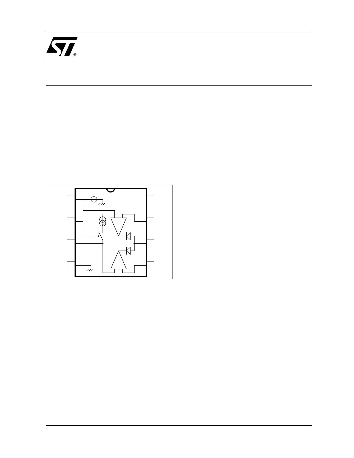
1 - TSM101 PRESENTATION
The TSM101 integrated circuit incorporates a high
stability series band gap voltage reference, two
ORed operational amplifiers and a current source
(Figure 1).
AN1283
APPLICATION NOTE
by S. LAFFONT and R. LIOU
A current limitation is used to prot ect the power
supply against short circuits, but lacks precision.
This limitation is generally realized by sensing the
current of the power transistor, in the primary side
of th e SMPS.
The role of the TSM101 is to make a fine
regulation of the output current of the SMPS and a
precise voltage limitation.
The primary current limitation is conserved and
acts as a security for a fail-safe operation if a
short-circuit occurs at the output of the charger.
Figure 1 : TSM101 Schematic Diagram
1.24V
1
CSEN
2
3
45
1.4mA
CRREF
GND CRIN
+
-
VCCVREF
8
-
VRIN
7
OUT
6
+
This IC compares the DC voltage and the current
level at the output of a switching power supply to
an internal reference. It provides a feedback
through an optocoupler to the PWM controller IC
in the primary side.
The controlled current generator can be used to
modify the level of current limitation by offsetting
the information comi ng from the cu rrent sensing
resistor.
A great majority of low or medium end power
supplies is voltage regulated by using shunt
programmable voltage references like the TL431
(Figure 2).
The galvanic insulat ion of the control information
is done by using an optocoupler in linear mode
with a variable photo current depending on the
difference between the actual output voltage and
the desired one.
2 - PRINCIPLE OF OPERATION
The current regulation loop and the voltage
limitation loop use an internal 1.24V band-gap
voltage reference. This voltage reference has a
good precision (better than 1.5%) and e xhibits a
very stable temperature behavior.
The current limitation is performed by sens i ng the
voltage across the low ohmic value resistor R
and comparing it to a fixed value set by the bridge
composed by R
When the voltage on R
on R
the output of the current loop operational
3
and R3 (Figure 3).
2
is higher than the voltage
5
amplifier decreases. The optocoupler current
increases and t ends t o reduc e the out put voltage
by the way of the PWM controller.
The voltage regulation is done by comparing a
part of the output voltage (resistor bridge R
6
, R
and P1) to the voltage reference (1.24V).
If this part is higher than 1. 24V, the output of the
voltage loop operational amplifier decreases.
The optocoupler current increases and tends to
reduce the output v oltage b y the way of the P WM
controller.
By enabling the TSM10 1 current source (pin 2) it
is possible to offset the current sensing by a
voltage equal to :
with I
= 1.4mA
0
V
OFF
R4I0⋅=
This offset lowers the output charge current and
this function can be used to charge two types of
batteries having different capacities. The current
source is enabled by connecting pin 2 to ground.
5
7
May 2001
1/7
Page 2

AN1283 - APPLICATION NOTE
V
V
3 - CALCULATION OF THE ELEMENTS
The charge current i s regulated at 700mA (if the
charge control input is left open) or 200mA (if the
charge control input is put to ground ), allowing the
charge of two different types of batteries.
3.1 Voltage limitation
The end-of-charge voltage is limited at 1.45V/c ell,
this is the recommended vol tage for an am bient
temperature at 25°C.
A diode is gene rally inserted at the output of the
charger to avoid the discharge of the battery if the
charger is not powered. This diode is sometimes
directly integrated in the battery pack. The
influence of this diode on the charge is negligible if
the voltage drop (0.7V) is taken into account
during the design of the charger.
The voltage at the output of the charger is :
R6R7+
V
OUT
and regarding R
R
which is a part of R6 and R7 is not considered
(P
1
-------------------- -
and R7 :
6
V
-----------------------------
6
V
outVref
V
⋅=
⋅=
ref
R
7
R
6
ref
+
in this equation)
The following values are used on the application
board :
❑ R
= 12kΩ
7
❑ R
= 1kΩ
6
❑ P
= 220Ω adjust for V
1
battery replaced by a 1kΩ resistor
❑ R
❑ C
= short circuit
10
= 100nF
3
= 15.2V with the
output
3.2 Current regulation
R
is the sense resistor used for current
5
measurement.
The current regulation is effective when the
voltage drop acros s R
is equal to the voltage on
5
pin 5 of the T SM101 (assuming that the interna l
current source is disabled).
For medium currents (<1A), a voltage drop across
R
of 200mV = VR5 is a good value, R5 can be
5
realized with standard low c ost 0.5W resistors in
parallel .
R
5
I
0.285Ω==
ch
R
5
----------
(four 1.2Ω resistor in parallel)
R
and R3 can be chosen using the following
2
formula :
–
R
6
refVR
---------------------------
⋅=
R
3
5
V
R
5
3.3 Charge control
If the pin 2 is left open, the charge current is
nominal at 700mA.
If pin 2 is connected to ground, the internal current
source is enabled, the current measurement is
offset by a voltage equal to :
I0R4⋅=
R
4
with I
= 1.4mA
0
V
This can be used to lower the charging current or
eventually to stop the charge, if V
> VR5.
R4
In our example, the current offset is equal to 700 200mA = 500mA, representing a voltage offset
V
= 140mV across R4.
R4
The following values are used on the application
board :
❑ R
= 300mΩ (four 1.2Ω-0.5W resistors in
5
parallel )
❑ R
= 100 Ω
4
❑ R
= 1.2k Ω
2
❑ R
= 220 Ω
3
❑ R
= short circuit
9
❑ R
= 10kΩ
1
❑ C
= 100nF
2
❑ C
= 100nF
5
❑ C
= output capacitor of the SMPS
1
❑ C
= 10µF
4
4 - SCHEMATIC DIAGRAM
Figure 2 represents a schematic of the output
circuit of a “classical” SMPS using a TL431 for
voltage regulation. This circuit is modified to use
the TSM101 and the final circuit is represented in
Figure 3.
2/7
Page 3
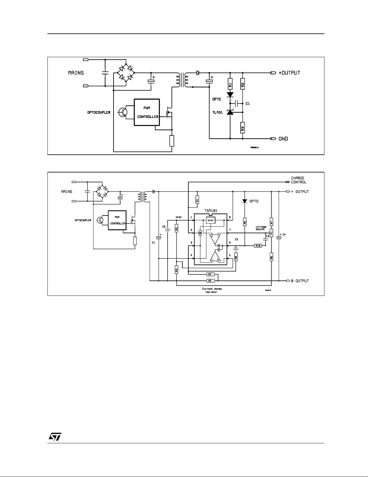
Figure 2 : SMPS Using a TL431 as Voltage Controller
Figure 3 : SMPS Using the TSM101
AN1283 - APPLICAT ION NOTE
5 - IMPROVEMENT
5.1. High frequency compensati on
Two R-C devices (R
, C2 and R10, C3) are used to
9
stabilize the regulation at high frequencies.
The calculation of these values is not easy and is
a function of the transfer function of the SMPS.
A guess value for the capacitors C
and C3 is
2
100nF.
5.2. Power supply for TSM101
In applications requiring low voltage battery
charge or when the charger is in current regulation
mode, the output voltage can be too low to supply
correctly the TSM101. The s ame problem occurs
when the output is short-circuited.
A solution to provide a quasi constant supply
voltage to th e TSM101 is s hown at Fig ure 4 : an
auxiliary winding is added at the secondary side of
the transformer.
This winding is forward coupled to the primary
winding, the voltage across it is directly
proportional to the mains rectified voltage, even if
the flyback voltage is close to zero.
As this auxiliar y winding is a voltage s ource, it is
necessary to add a resistor (R
of the rectifier (D
A low cost regulator (Q
) to limit the current.
3
and Zener diode D4) is
2
) on the cathode
11
used to power the TSM101. This is necessary with
autoranging SMPS with wide input voltages, for
example 90 to 240V without switching. In standard
SMPS with voltage range from 200 to 240V AC or
100 to 130VAC, this regulator can be removed
and replaced by the small power supply shown on
Figure 5 (R
aux
, C
aux
, D2).
3/7
Page 4

AN1283 - APPLICATION NOTE
Figure 4 : An Auxilia ry Win ding fo r TSM 101 P o wer Su pply
5.3 Higher Precision for the Voltage Control
The voltage drop through the sense resistor R
offsets the voltage measurement. In most battery
charging application s, this offset is not t aken into
account because the error is negligible compared
to the end-of-charge v oltage due to the fact that
the charging current value decreases drastically
during the final phase of the battery charging.
But in other applications needing highest possibl e
precision in voltage control, another connecting
schematic is possible for TSM101 as shown on
Figure 5.
In this schematic, the 0V reference is defined as
the common point between the sense resistor, the
0V Output Volt age, the foot of the res istor bridge
R
, and the ground (pin 4) of the TSM101.
6/R7
TSM101A (1% internal voltage reference
precision) is required in such applications.
5.4 An example of application where the
charging current is different according to the
charging phase.
The following application includes a specific
recommendation which requires that the charging
current should be fixed to I
charging conditions, and I
cell voltage is below V
low
= 800mA in normal
ch1
= 200mA when the
ch2
=2.5V to optimize the cell
life-time.
Moreover, a Charging Status LED should be
switched off when the cell voltage is above
V
=6.5V.
high
Figure 6 shows how this can ea sily be achieved
using an additional dual comparator (type LM393)
where the first operator (C
) is used to activate the
1
TSM101 internal current generator to offset the
current measurement thanks to R
5
second (C
) is used to switch the status LED off.
2
On Figure 6, the status signal is determined by
voltage measurement, this could as well be
achieved by current measurement.
If V
= 100mV is the maximum t olerable voltage
5
drop through the sense resistor R
during normal
5
charging conditions, then the following
calculations apply :
Current Control :
R
5
V
5
with R
R
+ R3 ~ 12kΩ and V
2
= 1kΩ, R2 = 11.4kΩ
3
V
5
V
---------- -
I
ch1
V
0.1V
5
------------
0.8A
R
3
-------------------- -
⋅=
ref
R2R3+
= 1.24V
ref
R4I0⋅ R5I
125mΩ== =
⋅+=
ch2
therefore,
with I
with V
R
0
low
= R14 = 10kΩ
15
V5R5I
----------------------------------- -
R
=
4
= 1.4mA, R4 = 53.6Ω
V
ref
V
low
= 2.5V and R14 + R15 ~ 20kΩ
⋅–
ch2
I
0
R
15
-------------------------- -
⋅=
R
+
14R15
, and the
4
4/7
Page 5

Figure 5 : Precise Output Voltage Control
AN1283 - APPLICAT ION NOTE
Figure 6 : Optimized Charging Conditions
5/7
Page 6

AN1283 - APPLICATION NOTE
EVALUATION BOARD - TECHNICAL NOTE
TSM101 integrates in the same 8 pin DIP or SO
package
❑ one 1.24V precision voltage reference
❑ two operational amplifiers
❑ two diodes which impose a NOR function
on the outputs of the operational amplifiers
❑ one current source which can be activated/
inhibited thanks to an external pin.
An immediate way to take ad vantage of the high
integration and reliability of TSM101 is to use it as
a voltage and current controller on power supplies
secondary. The application note AN1283
describes precisely how to use TSM101 in an
SMPS battery charger.
The TSM101 Evaluation Board is adaptable to any
power supply or battery charger (SMPS or linear)
as a voltage and current controller with minimal
constraints from the user.
HOW TO USE THE TSM101 EVALUA TION
BOARD ?
The generic Electrical Schematic is shown on
Figure 7. It represents an incomplete SMPS
power supply where the primary side is simplified.
The “IN+”and “IN-” power inputs of the
evaluation board shoul d be connected directly to
the power lines of the power supply secondary.
The “Vcc” input of the evaluation board should
be connected to the auxiliary supply line.
In the case of an SMPS power supply, the “Reg”
output of the evaluation board should be
connected to the Optocoupler input to regulate the
PWM block in the prim ary side. In the case of a
linear power supply, the “Reg” output should be
connected to the base of the darlington to regulate
the power output.
A diode might be needed on the output of the
evaluation board i n the case of a bat tery charger
application to avoid the discharge of the battery
when the charger is not connected.
COMPONENTS CALCULATIONS
The voltage co ntrol is given by the choice of the
resistor bridge R
(and the trimmer P1) due to
6/R7
equation 1 :
❑ V
where V
= R6/(R6+R7)xV
ref
= 1.24V
ref
eq1
out
The curren t control is given by the choice of the
voltage drop through the sense resistor R
(to be
5
linked to the nominal current of the application)
and by the value of the sense resistor itself.
Figure 7: Evaluation board schematic
6/7
Page 7

AN1283 - APPLICAT ION NOTE
For medium currents (< 1A ), a good value for t he
voltage drop through R
can be V
5
sense
= 200mV
(dissipation < 200mW).
The resistor bridge R
should be chosen
2/R3
following equation 2 :
❑ V
= R3 / (R2+R3) x V
sense
eq2
ref
The total value of t he resistor bridg e should be i n
the range of the kW in order to ensure a proper
charge for the voltage reference (in the range of
the mA).
To set the current limit, the sense resistor R
should be chosen following equation 3 :
❑ I
= V
lim
The internal current generator (I
/ R5 eq3
sense
) can be used
sce
to offset the current limitation with a lower value.
This current generator is activated by connecting
pin 2 to ground. It is inhibited if pin 2 is connected
to the positive rail via the pull up resistor R
.
1
The current offset is given by the choice of the
resistor R
If I
lim1
paragraph, and I
set when pin 2 is co nnecte d to ground, R
.
4
is the current limit calculated in the previous
is the current limit that is to be
lim2
should
4
be chosen following equation 4 :
❑ R
= (V
4
where I
C
and C5 are bypass capacitors used to
4
= 1.4mA
sce
sense
- I
lim2
x R5) / I
sce
eq4
smoothen the regulated outputs.
C
and C3 are capacitors used for high f requency
2
compensation.
5
Table 1
Voltage/
Current
Control
R1 10k
R2 1.2k
R3 220
R4 100
R5 1.2Ωx4 0.8Ωx4 1Ωx4
R6 1k
R7 12k
P1 100
2 straps 0
C2 100nF 100nF 100nF
C3 100nF 100nF 100nF
C4 10µF22
C5 100nF 100nF 100nF
15V
700mA
200mA
Ω
Ω
Ω
Ω
Ω
Ω
Ω
Ω
12V
1A
500mA
10k
Ω
1.2k
Ω
220
Ω
68
Ω
1k
Ω
8.2k
Ω
100
Ω
0
Ω
F 4.7µF
µ
8.2V
200mA
100mA
10k
1.2k
220
68
1k
5.6k
100
Figure 8
Ω
Ω
Ω
Ω
Ω
Ω
Ω
0
Ω
EXAMPLES OF COMPONENT LISTS
Table 1 summarizes a few examples of
component lists t o generate quickly 15V/700mA/
200mA, 12V/1A/500mA or 8.2V/200mA/100mA
voltage and current regulations.
Information furnished is bel ieved to be accurate and reliable. However, STMicroe lectronics assumes no responsibility for the
consequences of use of such information nor for any infringement of patents or other rights of third parties which may result from
its use. No li cense is granted by implica tion or otherwise under any patent or patent righ ts of S TMic roelec tronics. Specifications
mentioned in this publication ar e subject to change without notice. This publication supersedes and replaces all information
previously supplied. S TMicroelectronics products are not authorized for use as critica l components in life suppo rt devices or
systems without express written approval of STMicroelectronics.
Australi a - Brazil - China - Finland - France - Germany - Hong Kong - India - Italy - Japan - Malay sia - Malta - Morocco
© The ST logo is a registered trademark of STMicroelectronics
© 2001 STM icroelectronics - Prin ted in Italy - All Rights Reserved
STMicr o el ectronics GROU P OF COMPANIE S
Singapo re - Spain - Swe den - Switzerl and - United K i ngdom
© http://www.st.com
7/7
 Loading...