Page 1

PREAMPLIFIER AND SPEAKER DRIVER USING TS925
The TS925 is an input/output rail to rail quad B iCMOS operational amplifier. It is able to operate
with low supply voltages (2.7V) and to drive low
output loads such as 32Ω.
As an illustration of t hese features, the following
technical note highlights m any of the advantages
of the device in a global audio application.
APPLICATION CIRCUIT
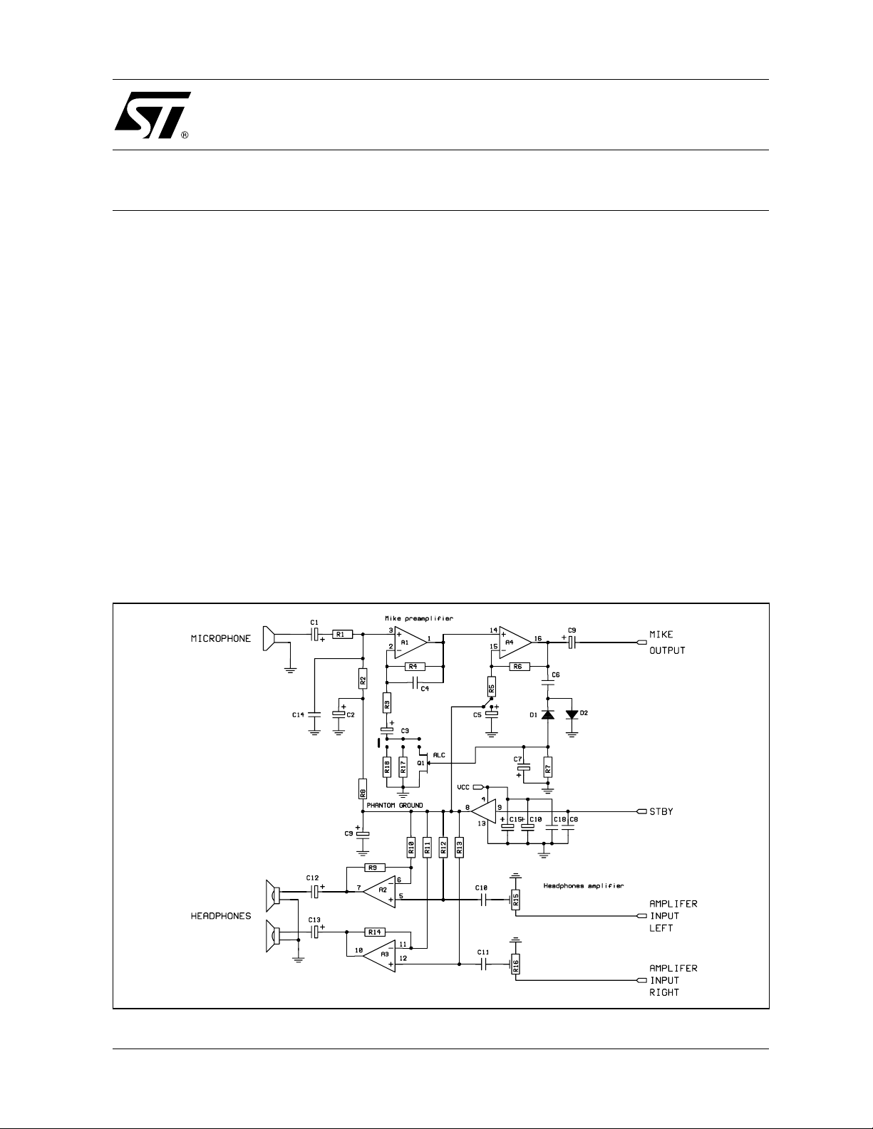
Figure 1 shows two operators (A1, A4) use d in a
preamplifier configuration, and the two others in a
push-pull configuration driving a headset.
The phantom ground i s used as a c ommon ref erence l evel (V
CC/2
).
AN1282
APPLICATION NOTE
by F. MARICOURT
Preamplifier : the operators A1 and A4 are wired
with a non inverting gain of respectively :
❑ A1# (R4/(R3+R17))
❑ A4# R6/R5
With the following values chosen :
❑ R4=22kΩ - R3 =50Ω - R17=1.2kΩ
❑ R6=47kΩ - R5 =1.2 kΩ,
the gain of the preamplifier chain is thus 58dB.
Alternatively, the gain of A1 can be adjusted by
choosing a JFET transistor Q1 instead of R17.
This JFET voltage controlled resistor arrangement
forms an automatic level control (ALC) circuit,
use-ful in many MIC preamplifier applications.
The power supp ly is delivered from two L R6 batter-ies (2x1.5V nominal).
Figure 1 : Electrical Schematic
The mean rectified peak level of the output signal
envelope is used to control the preamplifier gain.
June 2000
1/2
Page 2

AN1282 - APPLICATION NOTE
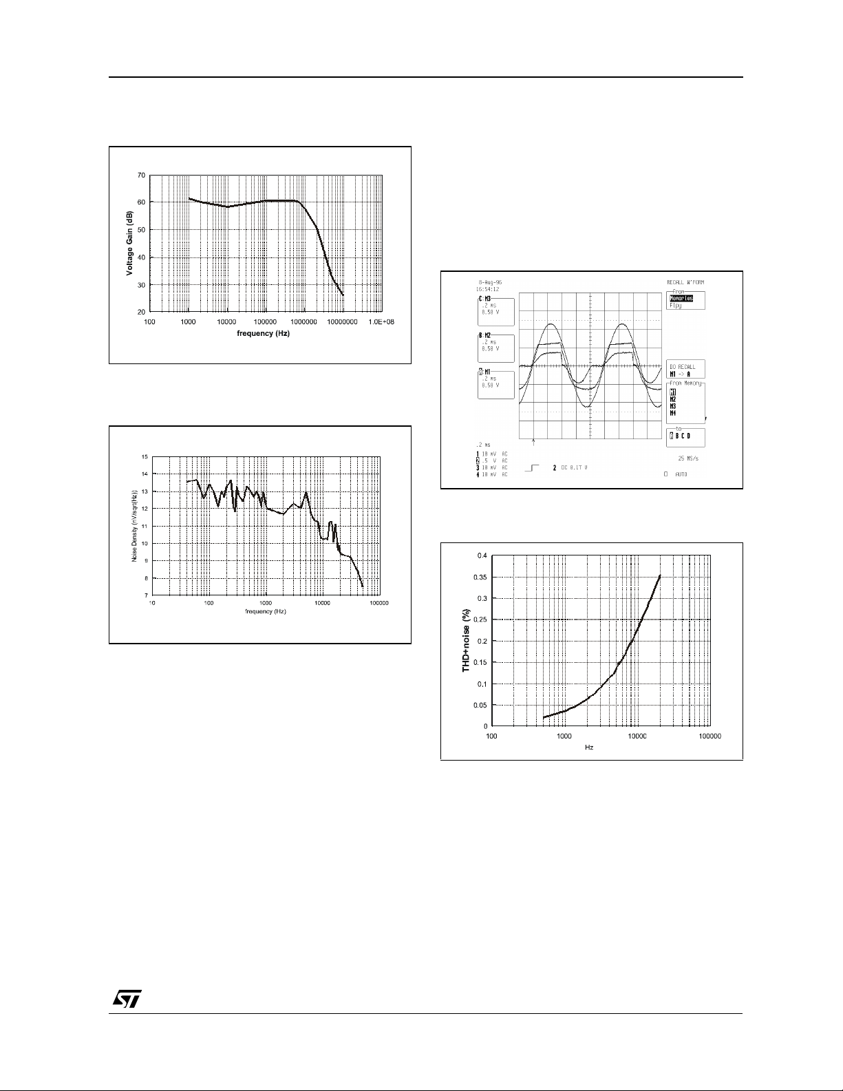
Figure 2 : Frequency Response of the Global
Preamplifier Chain
Figure 3 : Volta ge Noise De nsity versus
Frequency at Preamplifier Output
maximum o utput swing and a hi gh fidelity for reproducing sound and music.
Figure 4 shows the available signal swing at the
headset outputs : two other rail to rail competit or
parts are employe d in the sa me circuit for compari-40 Sson (note the much reduced clipping level and crossover distortion)
Figure 4 : Maximum Voltage Swing at
Headphone Outputs (R
) 32Ω)
L
Figure 5 : THD+Noise versus Frequency
(headphone outputs)
Headphone amp lifier : the operators A2 and A3
are organized in a push-pull configuration with a
gain of 5. The stereo inputs can be connected to a
CD-player and the TS925 drives directly the
head-phone speakers.This configuration shows
the abil-ity of the circuit to drive 32Ω load with a
Information furnished is bel ieved to be accurate and reliable. However, STMicroe lectronics assumes no responsibility for the
consequences of use of such information nor for any infringement of patents or other rights of third parties which may result from
its use. No li cense is granted by imp lica tion or otherwise under an y patent or patent rig hts of STMicroelectronics. Specific at ions
mentioned in this publication ar e subject to change without notice. This publication supersedes and replaces all information
previously supplied. S TMicroelectronics products are not authorized for use as critica l components in life suppo rt devices or
systems without express written approval of STMicroelectronics.
Australi a - Brazil - Chi na - Finland - F rance - Germany - Hong Kon g - I ndi a - Italy - Jap an - Malaysia - Malta - Morocco
© The ST logo is a registered trademark of STMicroelectronics
© 2000 STM icroelectronics - Printed in Ital y - All Rights Reserved
STMicr o el ectronics G ROU P OF COMPANIE S
Singapo re - Spain - Sweden - Switzerland - Un i ted Kingdom
© http://www.st.com
2/2
 Loading...