

Page 1
AN1281
APPLICATION NOTE
TS613 AS DRIVER FOR ADSL LINE INTERFACES - A SINGLE SU PPLY
IMPLEMENTATION WITH PASSIVE OR ACTIVE IMPEDANCE MATCHING
by C. PRUGNE
ADSL CONCEPT
Asymmetric Digital Subscriber Line (ADSL), is a
new modem technology, which converts the existing twisted-pair telephone lines into ac cess paths
for multimedia and high speed data communications.
ADSL transmits more than 8 Mbps to a subscriber,
and can reach 1Mbps from the subscriber to the
central office. ADSL can literally transform the actual public information network by bringing movies, television, video catalogs, remote CD-ROMs,
LANs, and the Internet into homes.
An ADSL modem is connected to a twisted-pair
telephone line, creating three information channels: a high speed downstream channel (up to
1.1MHz) depending on the implementation of the
ADSL architecture, a medium speed upstream
channel (up to 130kHz) and a POTS (Plain Old
Telephone Service), split off from the modem by
filters.
THE LINE INTERFACE - ADSL Remote
Terminal (RT):
The TS613 is used as a dual line driver for the upstream signal.
For the remote terminal it is required to create an
ADSL modem easy to plug in a PC. In such an application, the driver should be imple men ted with a
+12 volts single power supply. This +12V supply is
available on PCI connector of purchase.
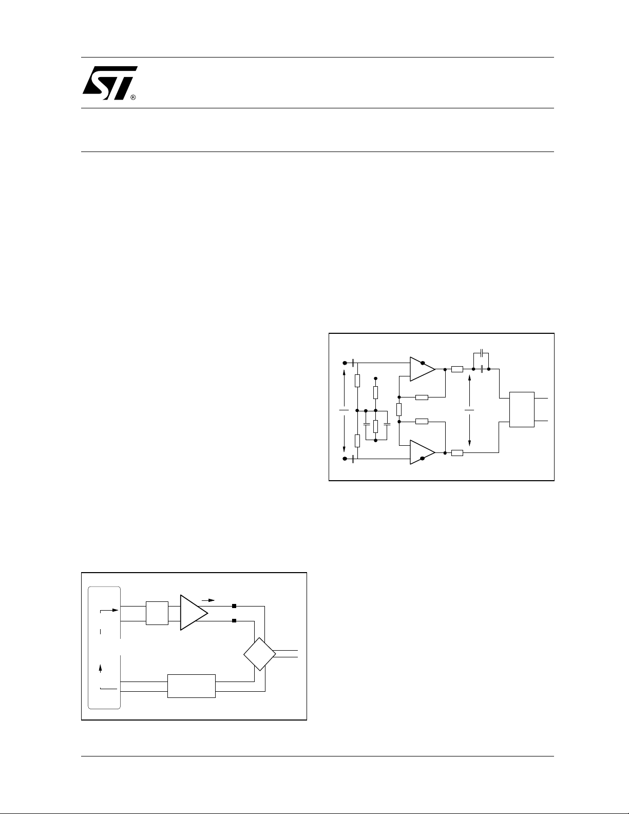
The figure 2 shows a single +12V supply circuit
that uses the TS613 as a remote terminal transmitter in differential mode.
Figure 2 : TS613 as a differential line driver with
a +12V single supply
100n
+12V
1k
Vi
Vi Vo
100n
10µ 100n
1k
GND
47k
47k
8
3
+12V
+
_
1
2
R2
R1
R3
_
6
7
5
+
GND
4
12.5
12.5
1µ
10n
Vo
1:2
Hybrid
&
Transformer
100Ω
Ω
25
The Figure1 shows a typ ical analog lin e interface
used for ADSL. The upstream and downstream
signals are separat ed from the telephone line by
using an hybrid circuit and a line transformer. On
this note, the accent will be made on the emission
path.
Figure 1 : Typical ADSL Line Interface
high output
current
digital to
analog
digital
treatment
analog to
digital
June 2000
emission
(analog)
reception
(analog)
LP filter
TS613
Line Driver
reception
circuits
upstream
impedance
matching
downstream
HYBRID
CIRCUIT
twisted-pair
telephone
line
The driver is biased with a m id supply (nominaly
+6V), in order to maintain the DC component of
the signal at +6V. Th is allows the maximum dy namic range between 0 and +12 V. Several options are possible to provide this bias supply (such
as a virtual ground using an operational amplifier),
such as a two-resistance divider which is the
cheapest solution. A high resistance value is required to limit the current consumption. On the
other hand, the current must be high enough to
bias the inverting input of the TS613. If we consider this bias current (5µA) as the 1% of the current
through the resistance divi der (500µA) to keep a
stable mid supply, two 47kΩ resistances can be
used.
The input provides two high pass filters with a
break frequency of about 1.6kHz whi ch is necessary to remove the DC component of the input signal. To avoid DC current flowing in the primary of
the transformer, an output capacitor is used.
1/3
Page 2
AN1281
The 1µF capacitance provides a path for low frequencies, the 10nF capacitance provides a path
for high end of the spectrum.
In differential mode the TS613 is able to deliver a
typical amplitude signal of 18V peak to peak.
The dynamic li ne i mpe danc e is 100Ω . The typical
value of the amplitude sign al required on the line
is up to 12.4V peak t o peak. B y us ing a 1 :2 transformer ratio the reflected impedance back t o the
primary will be a quarter (25Ω ) and therefore the
amplitude of the signal required with this impedance will be the half (6.2 V peak to peak). Assuming the 25Ω series resistance (12.5Ω for both outputs) necessary for impedance matching, the output signal amplitude required is 12.4 V peak to
peak. This value is acc eptable for the TS613. In
this case the load impedance is 25Ω for each driver.
For the ADSL up stream path, a lowpass filter is
absolutely necessary t o cuto ff the high er frequ encies from the DAC analog output. In this simple
non-inverting amplification configuration, it will be
easy to implement a Sallen-Key lowpass filter by
using the TS613. For AD SL over POTS, a maximum frequency of 135kHz is reached. For ADSL
over ISDN, the maximum frequency will be
276kHz.
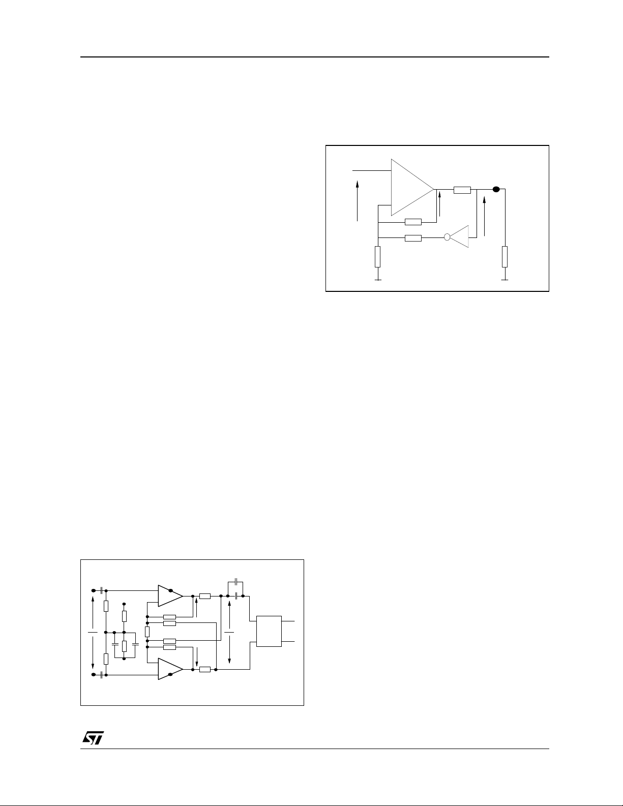
INCREASING THE LINE LEVEL BY USING AN
ACTIVE IMPEDANCE MATCHING
With passive matching, the output signal amplitude of the driver must be twice the amplitude on
the load. To go beyond this limitation an active
maching impedan ce can be used. With this tec hnique it is possible to keep good impedance
matching with an amplitude on the load higher
than the half of the oup ut driver amplitude. This
concept is shown in figure3 for a differential line.
Figure 3 : TS613 as a differential line driver with
an active impedance matching
100n
+12V
1k
Vi
Vi Vo
100n
10µ 100n
1k
GND
47k
47k
8
3
+12V
+
_
2
R2
R3
R1
R5
R4
_
6
5
+
4
GND
12.5
1
Vo°
Vo°
12.5
7
1µ
10n
Vo
1:2
Hybrid
&
Trans for mer
100Ω
Ω
25
Compon ent calculat i on:
Let us consider the equivalent c ircuit for a single
ended configuration, figure4.
Figure 4 : Single ended equivalent circuit
+
Rs1
Vi
1/2
Let us consider the unloaded system . Assuming
the currents through R1, R2 and R3
as respectively:
As Vo° equals Vo without load, the gain in this
case becomes :
The gain, for the loaded system will be (1):
GL
As shown in figure5, this system is an ideal generator with a synthesized impedance as the i nterna l
impedance of the system. From this, the output
voltage becomes:
with Ro the synthesized impedance and Iout the
output current. On the other hand Vo can be expressed a s:
Vo
_
R2
R1
G
Vo withload()
------------------------------------
R3
2
Vi Vo°
()
Vi
--------------------------
---------
,
1
R
Vo noload()
-------------------------------
==
Vi
Vi
Vo ViG()RoIout()
1
Vi
++
---------------------------------------------- -
1
Vo°
-1
–
2
R
Vi Vo
()
----------------------- -
and
1
++
-----------------------------------
1
++
1
-----------------------------------
-- -
2
–= 2
2R2
---------- -
–
2
R
------ -
1
3
R
R
2
R
------ -
3
R
Vo
+
3
R
2R2
---------- -
1
R
2
R
-------
1
–
3
R
2R2
---------- -
1
R
2
R
------ -
1
–
3
R
,
()
Rs1Iout
---------------------
R
------ -
1
–
R
1/2
RL
2
R
------ -
3
R
2
R
-------
3
R
1(),==
3(),–=
2
3
2/3
Page 3

AN1281
By identification of both e quat ions (2) a nd (3), the
synthesized impedance is, with Rs1=Rs2=Rs:
Figure 5 : Equivalent schematic. Ro is the syn-
thesized impedance
Ro
Iout
Rs
---------------- -
R
------ -
1
–
R
RL
1/2
4(),=
2
3
Ro
Vi.Gi
Unlike the level Vo° required for a passive impedance, Vo° will be smaller than 2Vo in our case. Let
us write Vo°=kVo with k the matching factor varying between 1 and 2. Assum ing that the current
through R3 i s negligeable, it comes the fo llowing
resistance divider:
Ro
RL2Rs
1+
kVoRL
---------------------------
=
After choosing the k factor, Rs will equal to
1/2RL(k-1).
A good impedance matching assume s:
1
-- -
Ro
,=
RL5()
2
From (4) and (5) it becomes:
R
------ -
R
2
3
2
Rs
--------- -
1
RL
6(),–=
By fixing an arbitrary value for R2, (6) gives:
R
1
2
Rs
--------- -
–
RL
2
R
-------------------
3
=
Finally, the values of R2 and R3 allow us to extract
R1 from (1), and it comes:
---------------------------------------------------------
1
R
21
2R2
2
R
------ -
–
R
3
GL
7(),=
2
R
------ -
1–
–
3
R
with GL the required gain.
GL (gain for the
loaded system)
R1 2R2/[2(1-R2/R3)GL-1-R2/R3]
R2 (=R4) Abrit ra ry fixed
R3 (=R5) R2/(1-Rs/0.5RL)
Rs 0.5RL(k-1)
GL is fixed for the application requirements
GL=Vo/Vi=0.5(1+2R2/R1+R2/R3)/(1-R2/R3)
CAPABILITIES
The table below shows the calculated components for different values of k. In this case
R2=1000Ω and the gain=16dB. The last column
displays the maximu m amplitude level on the line
regarding the TS613 maximum output capabilities
(18Vpp diff.) and a 1:2 line transformer ratio.
Active matching
TS613 Output
R1
k
(Ω)R3(Ω)Rs(Ω)
1.3 820 1500 3.9 8 27.5
1.4 490 1600 5.1 8.7 25.7
1.5 360 2200 6.2 9.3 25.3
1.6 270 2400 7.5 9.9 23.7
1.7 240 3300 9.1 10.5 22.3
Passive matching 12.4 18
Level to get
12.4Vpp on
the line
(Vpp diff)
Maximum
Line level
(Vpp diff)
MEASUREMENT OF THE POWER
CONSUMPTION IN THE ADSL APPLICATION
Conditions:
Passive impedance matching
Transformer turns ratio: 2
Maximun level required on the line: 12.4Vpp
Maximum output level of the driver: 12.4Vpp
Crest factor: 5.3 (Vp/Vrms)
The TS613 power consumption during em ission
on 900 and 4550 meter twisted pair telephone
lines: 360mW
Information furnished is bel ieved to be accurate and reliable. However, STMicroe lectronics assumes no responsibility for the
consequences of use of such information nor for any infringement of patents or other rights of third parties which may result from
its use. No li cense is granted by i mp lication or otherwise under any patent or pate nt rights of STMicroelectronics. Specifications
mentioned in this publication ar e subject to change without notice. This publication supersedes and replaces all information
previously supplied. S TMicroelectronics products are not authorized for use as critica l components in life suppo rt devices or
systems without express written approval of STMicroelectronics.
Australi a - Brazil - Chi na - Finlan d - F rance - Germ any - Hong Kong - India - Ital y - Japan - Ma l aysia - Malta - Morocco
3/3
© The ST logo is a registered trademark of STMicroelectronics
© 2000 STM icroelectronics - P rinted in Italy - All Righ ts Reserv ed
STMicr o el ectronics GROUP OF COMPA NI E S
Singapo re - Spain - Sweden - Swit zerland - Un ited Kingd om
© http://www.st.com
 Loading...