

Page 1
AN1256
Application note
High-power RF MOSFET targets VHF applications
Introduction
The SD2933, which utilizes a double-diffused metal oxide (DMOS) semiconductor
technology, is the latest addition to STMicroelectronics’ RF Power MOSFET family. The
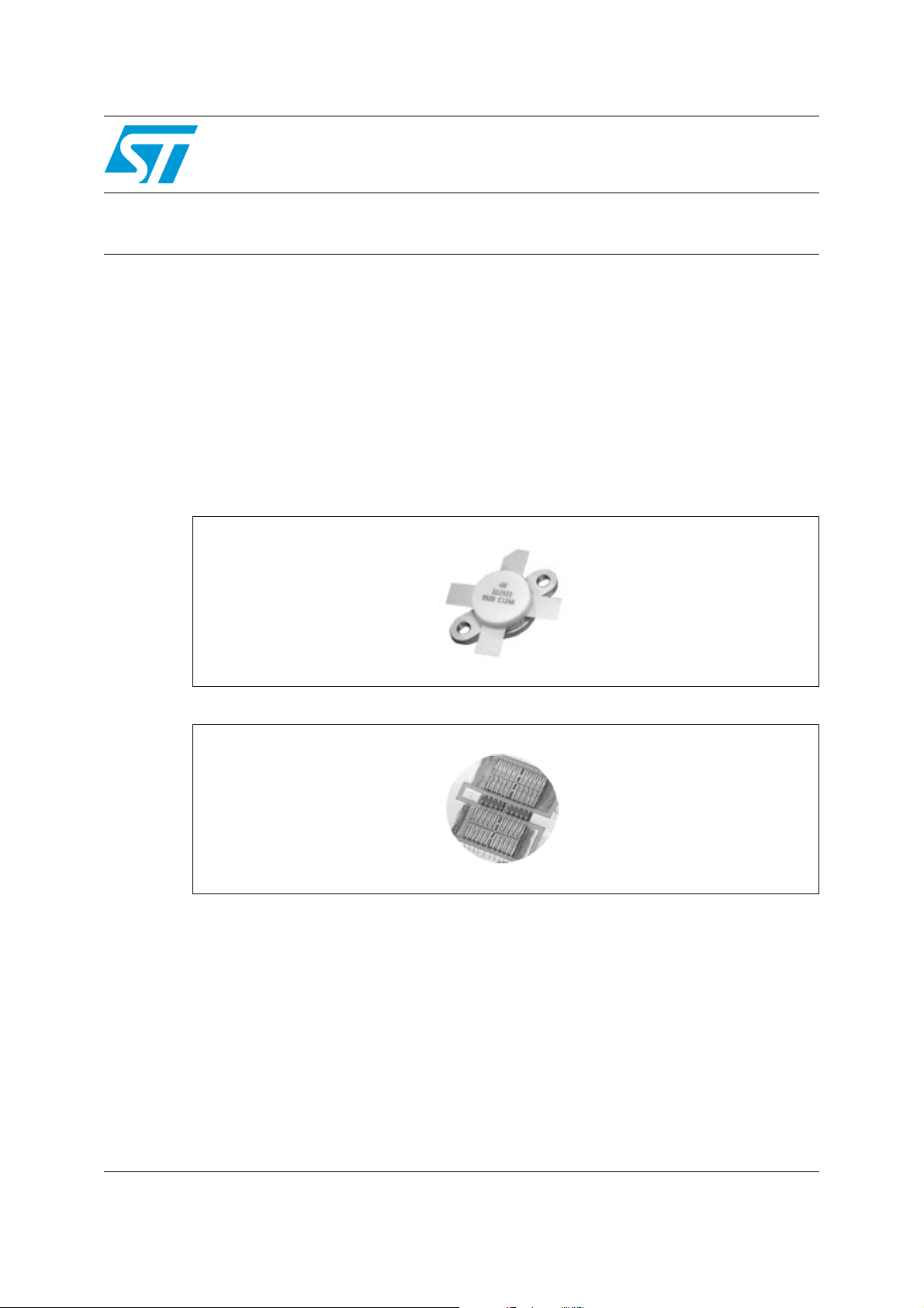
packaged version is shown in Figure 1. The SD2933 is a single-ended, 50 V, 300 W, gold
(Au) metallized, N-channel, vertical Power MOSFET, intended for use up to 150 MHz, with
exceptionally high gain, and enhanced thermal packaging which makes it ideal for various
applications including plasma generation, excitation and FM broadcast applications. The
unique design of this single-ended 300 W Power MOSFET, makes it the only one of its class
available on the market today.
Figure 1. SD2933 Package
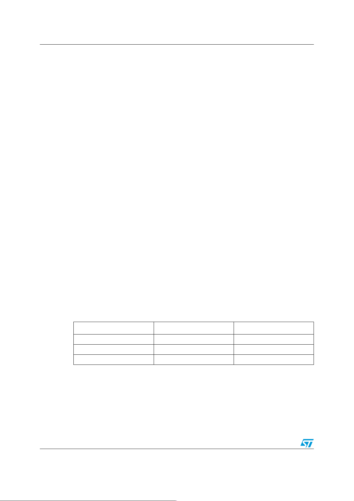
Figure 2. Two Enhancement - mode DMOS mounted in parallel
July 2007 Rev 2 1/7
www.st.com
Page 2
Device assembly AN1256
1 Device assembly
The SD2933 discrete component design consists of two 40 cell, N-channel, enhancement
mode DMOS transistor dice eutectically mounted in a parallel configuration (see Figure 2).
Each cell consists of 60, 127 µm gate fingers, yielding a source periphery of 1220 mm
allowing a maximum drain current of 40 A. The transistor dice are separated by a metallized
gate rail on which two, thin film, Au metallized resistors are eutectically mounted. For
improved current capability and lower inductance, the components are connected to each
other and to the package by Au wire with a diameter of 2 mils (50 µm). Since the dice and
package utilize gold metallization and the bonding wires are also gold, reliability issues
pertaining to the contact of dissimilar metals between wire, package, and die are eliminated.
The package is sealed with a ceramic lid ensuring the complete integrity of the wires and
silicon die and also preventing any foreign objects from entering the package which could
ultimately cause device reliability problems.
2 Device characteristics
The SD2933 has a very high transconductance. The transconductance (gfs) denotes the
DC gain of a Power MOSFET. It is defined as the ratio of the infinitesimal change in drain
current corresponding to the infinitesimal change in gate voltage at a specified current level
and drain bias. It is important to measure the gfs in the device’s region of operation where
the gfs is independent of the drain bias (VDS). The gfs of the SD2933 measured at a drainsource voltage of 10 V and a corresponding drain current of 10 A, is typically 13 siemens.
Impedance data across a range of frequencies may be the most important information an
amplifier designer needs. Without it, the RF performance may not come close to the
published values found in the datasheet. With properly measured data, and sound
impedance matching techniques, many frustrating hours of circuit design iterations can be
saved.
For this reason, the following impedances were measured to help in the design of amplifiers
for the HF, FM broadcast, and plasma generation markets as shown in Figure 1.
Table 1. Impedance data for the design of amplifiers
Frequency (MHz) ZIN(Ω) ZDL(Ω)
30 1.8 - j0.2 2.8 + j2.3
108 1.9 + j0.2 1.6 + j1.4
175 1.9 + j0.3 1.5 + j1.6
One important item to note is the relatively small change in input impedance from 30 MHz to
150 MHz. This can be attributed to the series gate resistors which present a real impedance
at the input across the full band of frequencies. Matching is easily accomplished by using
transmission line transformers and lumped elements commonly found in many amplifiers.
The SD2933 was characterized in a common source mode at 30 MHz with a circuit
optimized for best return loss and maximum power delivered to the load with a typical gain
and efficiency of 23.5 dB and 65% respectively, as shown in Figure 3. The junction to case
thermal resistance (R
2/7
) was measured under RF operating conditions using infrared
TH-JC
Page 3
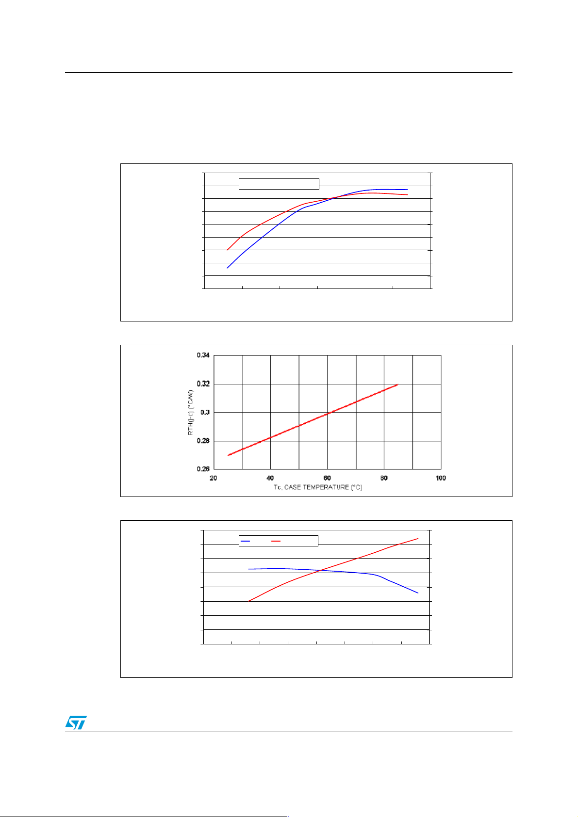
AN1256 Device characteristics
techniques to be 0.27 °C/W allowing for a maximum power dissipation of approximately
650 W (see Figure 4).
Additionally, data was taken at 150 MHz demonstrating the gain and efficiency at the upper
limits of the device characterization (see Figure 5).
Figure 3. Power Gain and efficiency vs. output power
450
400
350
300
250
200
150
Output power (W)
100
50
0
0 0.5 1 1.5 2 2.5 3
Pout Efficiency
Input power (W)
90
80
70
60
50
40
30
Efficiency (%)
20
10
0
Figure 4. Maximum thermal resistance vs. case temperature
Figure 5. Power gain and efficiency vs. output power
27
26
25
24
23
22
Gain (dB)
21
20
19
0 50 100 150 200 250 300 350 400
Gain Efficiency
Output power (W)
80
70
60
50
40
30
Efficiency (%)
20
10
0
3/7
Page 4

Device ruggedness AN1256
3 Device ruggedness
The SD2933 is very rugged. Most DMOS failures during operating conditions are due to the
inability to support the effective drain voltage across the body-drain pn junction during an
overvoltage condition when, for example, a mismatched load causes a large voltage
standing wave on the drain terminal. If the device is subjected to an excessive drain to
source voltage, the electric field across this junction reaches a critical value at which point
avalanche current is generated. Under these conditions, current flows from the source to the
body, effectively biasing the internal parasitic bipolar transistor to an on-state, creating a
catastrophic failure very quickly. The voltage required to turn on the parasitic transistor has a
negative temperature coefficient, thus at higher operating temperatures this phenomena is
more likely. It can be noted that some manufacturers of high power RF devices do not
specify a load mismatch, but the SD2933 is guaranteed to sustain a 5:1 load mismatch
across all phase angles with no degradation in output power when returned to 50 ohms.
This load mismatch is comparable to devices with similar output power levels utilizing a
push-pull package configuration. The ability of the SD2933 to handle such a severe
mismatch can be attributed to two design improvements over similar devices. The first being
a proprietary doping scheme of the transistor die during its fabrication process, which allows
high current and voltage swings without inducing turn-on of the internal parasitic bipolar
transistor, and the second enhancement is the lower thermal resistance of the packaging
allowing for increased power dissipation of the device. These considerations result in a very
high breakdown voltage minimum rating of 125 V, with a normal distribution of 145 V DC.
4 Design considerations
Designing the SD2933 offered two distinct challenges beyond the semiconductor device
design; one was due to the high gain of the SD2933 in the HF frequency band, and the other
was due to the high power dissipation of this single ended device. The gfs of this device is
very high thus, stabilizing the transistor was extremely critical. Without the use of any
stabilization technique, the device would oscillate and destroy itself under bias conditions
before the RF input was applied. To overcome potential instabilities, gate resistors were
employed. These resistors, as mentioned before, are eutectically mounted inside the
package along with the transistor die and are wired in series with each gate pad. This layout
presents a series resistance to each gate site and thus any difference between the site to
site impedances are small relative to the total.
4/7
Page 5
AN1256 MTTF (mean time to failure) enhanced package
5 MTTF (mean time to failure) enhanced package
A major problem inherent to high power RF transistors is their high operating junction
temperatures. If careful consideration is not taken to remove the heat generated by the
junction, degradation in device performance and reduction in its operating lifetime are the
consequences. The design of the SD2933 has solved this problem by using a thermally
enhanced package, labeled a non-pedestal (NP) package, having lower thermal resistance
than the widely used pedestal (P) packages. A finite-element analysis was performed on a
similar NP package and the results showed a 10 °C lower peak temperature than the P
package under the same thermal conditions. The SD2931-10 and a similar ST device were
then chosen to further demonstrate the enhanced thermal properties of the NP package
over the P package under normal operating conditions. These devices use the same
transistor die and also share the same overall mechanical dimensioning. The major
difference between the devices is that the SD2931-10 is a NP package and the other was a
P package. Both devices were operated under RF conditions and their corresponding die
junction temperatures were measured using an infrared (IR) imaging unit. Once again the
results were in favor of the NP package with a 25% improvement in thermal resistance
which corresponds to an operating life improvement of approximately 400%.
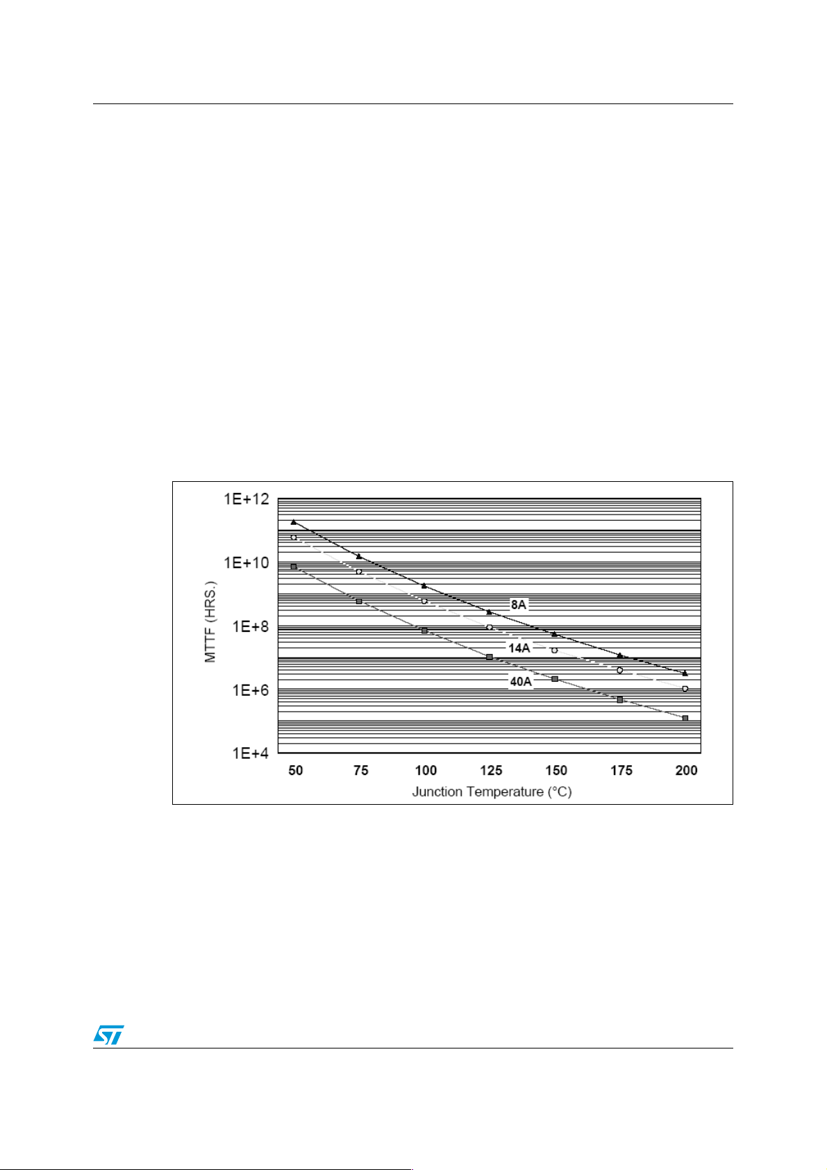
Figure 6. SD2933 MTTF for various currents as a function of junction temperature
Electromigration is another temperature-enhanced failure mechanism. Electromigration
failures are related to current density in the metallization as well as other metallization
material properties. A graph of the SD2933 mean-time-to-failure, for various currents as a
function of junction temperature, based on the electromigration activation energy derived
from Arrhenius plots for the SD2933, is shown in Figure 6. It can be seen that the typical
lifetime is greater than 1 million hours.
It should be noted that in comparison, the SD2933 is a larger device than the SD2931-10,
but the overall structure of the SD2933 package and the SD2931-10 package are the same
and both devices use the same transistor die. For a complete thermal analysis of the P vs.
5/7
Page 6

Revision history AN1256
NP packages, please refer to the April 1999 issue of Microwaves & RF titled "Novel Package
Improves Power MOSFET Reliability".
For complete documentation on the SD2933, the datasheet can be found on the
STMicroelectronics website: www.st.com. Enter SD2933 in the “search part number” field in
the upper right-hand corner of the page.
6 Revision history
Table 2. Revision history
Date Revision Changes
21-Mar-2000 1 First issue
– Figure 3 and Figure 5 changed
30-Jul-2007 2
– Minor text changed
– The document has been reformatted
6/7
Page 7

AN1256
Please Read Carefully:
Information in this document is provided solely in connection with ST products. STMicroelectronics NV and its subsidiaries (“ST”) reserve the
right to make changes, corrections, modifications or improvements, to this document, and the products and services described herein at any
time, without notice.
All ST products are sold pursuant to ST’s terms and conditions of sale.
Purchasers are solely responsible for the choice, selection and use of the ST products and services described herein, and ST assumes no
liability whatsoever relating to the choice, selection or use of the ST products and services described herein.
No license, express or implied, by estoppel or otherwise, to any intellectual property rights is granted under this document. If any part of this
document refers to any third party products or services it shall not be deemed a license grant by ST for the use of such third party products
or services, or any intellectual property contained therein or considered as a warranty covering the use in any manner whatsoever of such
third party products or services or any intellectual property contained therein.
UNLESS OTHERWISE SET FORTH IN ST’S TERMS AND CONDITIONS OF SALE ST DISCLAIMS ANY EXPRESS OR IMPLIED
WARRANTY WITH RESPECT TO THE USE AND/OR SALE OF ST PRODUCTS INCLUDING WITHOUT LIMITATION IMPLIED
WARRANTIES OF MERCHANTABILITY, FITNESS FOR A PARTICULAR PURPOSE (AND THEIR EQUIVALENTS UNDER THE LAWS
OF ANY JURISDICTION), OR INFRINGEMENT OF ANY PATENT, COPYRIGHT OR OTHER INTELLECTUAL PROPERTY RIGHT.
UNLESS EXPRESSLY APPROVED IN WRITING BY AN AUTHORIZED ST REPRESENTATIVE, ST PRODUCTS ARE NOT
RECOMMENDED, AUTHORIZED OR WARRANTED FOR USE IN MILITARY, AIR CRAFT, SPACE, LIFE SAVING, OR LIFE SUSTAINING
APPLICATIONS, NOR IN PRODUCTS OR SYSTEMS WHERE FAILURE OR MALFUNCTION MAY RESULT IN PERSONAL INJURY,
DEATH, OR SEVERE PROPERTY OR ENVIRONMENTAL DAMAGE. ST PRODUCTS WHICH ARE NOT SPECIFIED AS "AUTOMOTIVE
GRADE" MAY ONLY BE USED IN AUTOMOTIVE APPLICATIONS AT USER’S OWN RISK.
Resale of ST products with provisions different from the statements and/or technical features set forth in this document shall immediately void
any warranty granted by ST for the ST product or service described herein and shall not create or extend in any manner whatsoever, any
liability of ST.
ST and the ST logo are trademarks or registered trademarks of ST in various countries.
Information in this document supersedes and replaces all information previously supplied.
The ST logo is a registered trademark of STMicroelectronics. All other names are the property of their respective owners.
© 2007 STMicroelectronics - All rights reserved
STMicroelectronics group of companies
Australia - Belgium - Brazil - Canada - China - Czech Republic - Finland - France - Germany - Hong Kong - India - Israel - Italy - Japan -
Malaysia - Malta - Morocco - Singapore - Spain - Sweden - Switzerland - United Kingdom - United States of America
www.st.com
7/7
 Loading...