

Page 1

AN1246
Application note
VIPower: auxiliary BIAS
power supply using VIPer20A-E
Introduction
This application note describes a bias power supply to meet the needs of powering up
Power MOSFETs as well as providing standby power when the main unit is off.
The VIPer20ADIP-E, a part of STMicroelectronics proprietary VIPower (Vertical Intelligent
Power), is a current mode PWM with a 700 V avalanche rugged Power MOSFET. It uses a
fabrication process which allows the integration of analog control circuits with a vertical
power device on the same chip. It can provide an output of 10 W power capability for wide
range input, or 20 W for single input voltage range.
October 2007 Rev 4 1/8
www.st.com
Page 2

Contents AN1246
Contents
1 Key features of the VIPer20ADIP-E . . . . . . . . . . . . . . . . . . . . . . . . . . . . . 3
2 General circuit description . . . . . . . . . . . . . . . . . . . . . . . . . . . . . . . . . . . . 3
3 Connecting the demoboard . . . . . . . . . . . . . . . . . . . . . . . . . . . . . . . . . . . 6
4 Layout considerations . . . . . . . . . . . . . . . . . . . . . . . . . . . . . . . . . . . . . . . 6
5 Burst mode . . . . . . . . . . . . . . . . . . . . . . . . . . . . . . . . . . . . . . . . . . . . . . . . 6
6 Performance and cost consideration . . . . . . . . . . . . . . . . . . . . . . . . . . . 7
7 Revision history . . . . . . . . . . . . . . . . . . . . . . . . . . . . . . . . . . . . . . . . . . . . 7
2/8
Page 3
AN1246 Key features of the VIPer20ADIP-E
1 Key features of the VIPer20ADIP-E
■ Adjustable switching frequency up to 200 kHz
■ Current mode control
■ Burst mode operation in standby mode, meets “Blue Angel” standards
■ Undervoltage lock-out with hysteresis
■ Integrated start-up supply
■ Avalanche rugged
■ Overtemperature protection
■ Primary or secondary regulation general circuit description
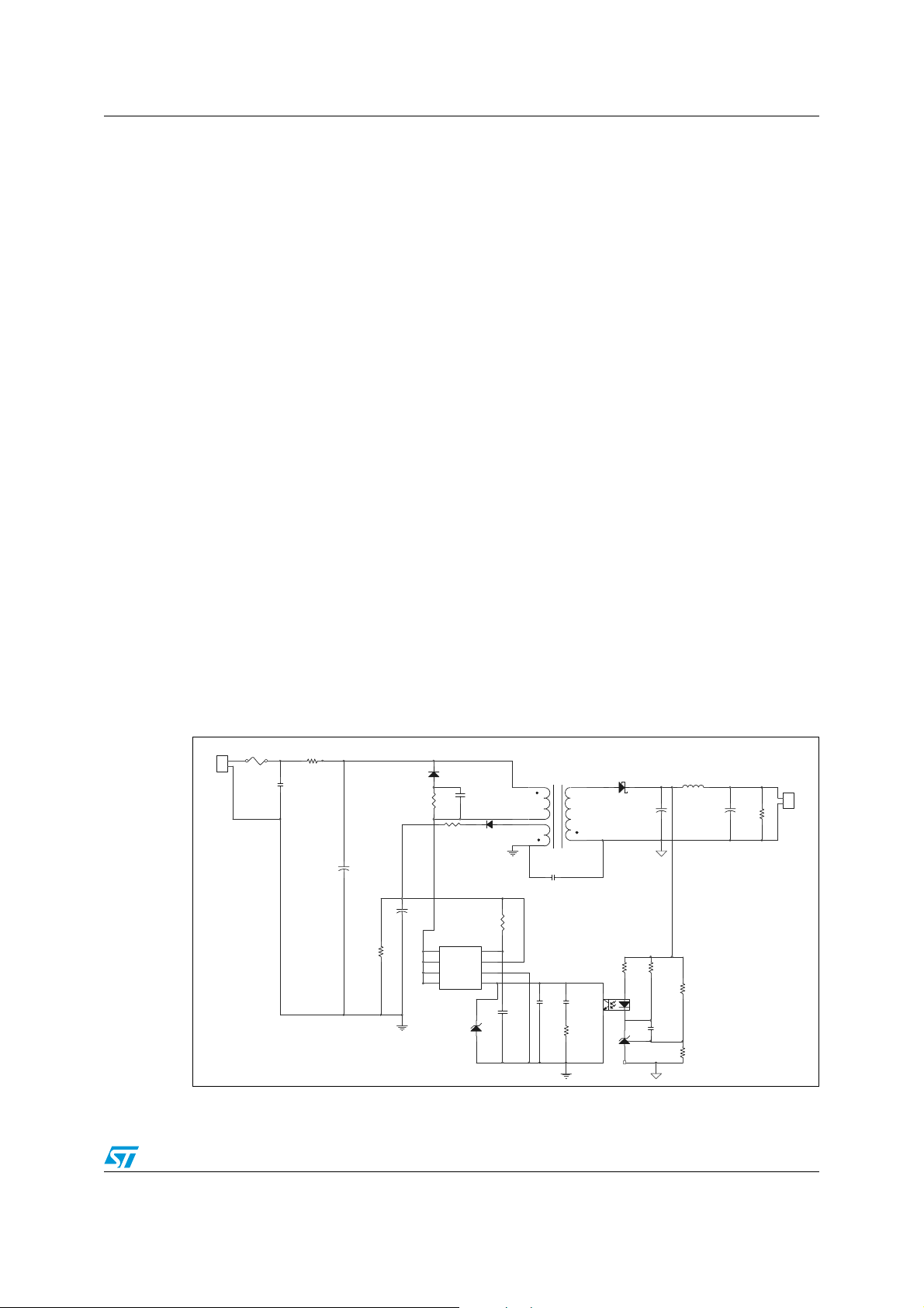
2 General circuit description
This demo board (see schematic in Figure 1) is a 110 to 375 VDC input discontinuous
flyback, working at 100 kHz. The output can deliver 12 V at 0.5 A continuous. This circuit
can be powered from the main bulk capacitors of an off-line power supply, power factor
correction output stage, or the AC line with the addition of a low current bridge rectifier. It
benefits from the EMI filter present in a typical power supply. The output uses a Schottky
diode for better efficiency. C7 is a low ESR capacitor which manages the ripple current. IC2
provides the reference and the feedback to tightly regulate the output. CS5, CS6, and RS3
form the feedback loop compensation to optimize stability during transients. The demoboard
can be tested with convection air. Depending on the final application, air flow might be
needed to keep the VIPer20ADIP-E under the thermal shutdown limit.
Figure 1. Schematic
CON
J1
2
1
F1
0.5 A Pico Fuse
R9
3.9
C12
220pF
1KV
D1
BYT11-600
C10
RS14
220pF
82K
1KV
RS4
DS3
1.6
LL4148
C2
4.7uF
400V
C3
120uF
16V
IC1
RS10
nu
8
7
6
drain
drain
drain
VIPer20ADIP-E
source
1
osc
2
vdd
3
45
compdrain
D4
NU
Cramer Coil CSM 1608-027
4
128T
3
2
14T
1
RS2
4.99K
CS4
3.9nF
T1
c9
2.2n
Y cap
CS5
33n
DS2
6
STPS1H100A
16T
7
CS6
.47u
RS3
5.1k
C7
680uF
16V
R6
150
12
43
IC3
H11A817A
IC2
TL431
R
A C
L2
10uH
R8
1.2k
R7
5.23k
CS11
47n
RS5
1.37k
C8
330uF
16V
J2
1
2
R11
CON
2.7k
3/8
Page 4

General circuit description AN1246
Table 1. Electrical specification from measured results
Parameter Results
Input voltage range J1 110 to 375 V
DC
Output J2 12 V from 0 to 0.5 A
Load regulation (0 to 0.5 A) from setpoint +/-25 mV or +/-0.2%
Line regulation (at max load) +/-1 mV
Efficiency 84% at 120 V
and 79% at 375 V
DC
Output ripple voltage 35 mV MAX
Input power at no load 0.65 W MAX
Transient response, 50% load step +/-60 mV typical
Figure 2. PC board top legend bottom foil and surface mount components
DC
Table 2. Component list
Quantity Reference Description Value
1 C2 F4.7 µF 400 V
1 C3 120 µF 16 V (low ESR)
1 CS4 3.9 nF 50 V
1 CS5 33 nF 50 V
1 CS6 47 µF 25 V
1 C7 680 µF 16 V (low ESR)
1 C8 330 µF 16 V (low ESR)
1 C9 Y1 Rated safety cap 2.2 nF
1 C10 220 pF 1 KV
1 CS11 47 µF 50 V
1 C12 220 pF 1 KV
1 D1 BYT11-600
4/8
(1)
600 V 1 A Ultrafast
Page 5

AN1246 General circuit description
Table 2. Component list (continued)
Quantity Reference Description Value
1 DS2 STPS1H100A
1 DS3 LL4148
1 F1 fuse 0.5 A pico
1 IC1 VIPer20ADIP-E
1 IC2 TL431
1 IC3 H11A817A (optocoupler)
1 J1 Connector terminal
1 J2 Connector terminal
1 L2 Coilcraft PCH-27-103 10 µH
1 RS2 4.99 KΩ 1% 1/8 W
1 RS3 5.1 KΩ 1/8 W
1 RS4 1.6 Ω 1/8 W
1 RS5 1.37 Ω 1% 1/8 W
1 R6 150 Ω 1/4 W
1 R7 5.23 KΩ 1% 1/4 W
(1)
100 V 1 A Schottky
(1)
(1)
1 R8 1.2 KΩ 1/4 W
1 R9 3.9 Ω 1/4 W
1 R11 2.7 KΩ 1/4 W
1 RS14 82 KΩ 1/4 W
1 T1 Cramer Coil CSM 1608-027
1. Parts available from STMicroelectronics. “S” in legend denotes a surface mount part.
Table 3. Transformer specification
Parameter Value
Primary inductance 1.65 mH
Core C40 EE16
Figure 3. Cross section of the transformer
5/8
Page 6

Connecting the demo board AN1246
3 Connecting the demo board
This demo board has two connectors. Connect a DC voltage source capable of delivering up
to 400 volts DC to connector J1. Be sure to connect the positive source to the + terminal of
J1 and the negative to the terminal before turning on the input power. The minimum voltage
to operate this demo board is 110 V
. Connect an electronic load or resistive load to J2.
DC
4 Layout considerations
Some simple rules to improve performance and minimize noise should be followed:
1. Minimize power loops. The switched power current paths inner loop area must be as
small as possible. This can be accomplished by careful layout of the printed circuit
board and the use of surface mount components. This avoids radiated and conducted
EMI noise, and improves the efficiency by eliminating parasitic inductance, thus
reducing or eliminating the need for snubbers and EMI filtering.
2. Use separate tracks for low level signal and power traces carrying fast switching pulses.
This can be seen on the VIPer20ADIP-E pin 3 on the printed circuit lay out. When
signal paths share the same trace as a power path, instabilities may result. The
compensation components, CS6, RS3, and CS4 are on a separate trace connected
directly to the source of the device.
5 Burst mode
When the output current is too low, the burst mode operation takes over automatically. This
results in missing cycles as shown on the following scope waveform (Figure 4). V
V
DC IOUT
As can be seen, there is one pulse out of ten pulses to reduce power consumption. The
output ripple is negligible.
is at no load.
is 375
in
6/8
Page 7

AN1246 Revision history
Figure 4. Burst mode waveform
6 Revision history
Table 4. Document revision history
Date Revision Changes
04-Jan-2004 3 Minor text changes
18-Oct-2007 4
– Document reformatted no content change
– VIPer20A replaced by VIPer20A-E
– VIPer20ADIP replaced by VIPer20ADIP-E
7/8
Page 8

AN1246
Please Read Carefully:
Information in this document is provided solely in connection with ST products. STMicroelectronics NV and its subsidiaries (“ST”) reserve the
right to make changes, corrections, modifications or improvements, to this document, and the products and services described herein at any
time, without notice.
All ST products are sold pursuant to ST’s terms and conditions of sale.
Purchasers are solely responsible for the choice, selection and use of the ST products and services described herein, and ST assumes no
liability whatsoever relating to the choice, selection or use of the ST products and services described herein.
No license, express or implied, by estoppel or otherwise, to any intellectual property rights is granted under this document. If any part of this
document refers to any third party products or services it shall not be deemed a license grant by ST for the use of such third party products
or services, or any intellectual property contained therein or considered as a warranty covering the use in any manner whatsoever of such
third party products or services or any intellectual property contained therein.
UNLESS OTHERWISE SET FORTH IN ST’S TERMS AND CONDITIONS OF SALE ST DISCLAIMS ANY EXPRESS OR IMPLIED
WARRANTY WITH RESPECT TO THE USE AND/OR SALE OF ST PRODUCTS INCLUDING WITHOUT LIMITATION IMPLIED
WARRANTIES OF MERCHANTABILITY, FITNESS FOR A PARTICULAR PURPOSE (AND THEIR EQUIVALENTS UNDER THE LAWS
OF ANY JURISDICTION), OR INFRINGEMENT OF ANY PATENT, COPYRIGHT OR OTHER INTELLECTUAL PROPERTY RIGHT.
UNLESS EXPRESSLY APPROVED IN WRITING BY AN AUTHORIZED ST REPRESENTATIVE, ST PRODUCTS ARE NOT
RECOMMENDED, AUTHORIZED OR WARRANTED FOR USE IN MILITARY, AIR CRAFT, SPACE, LIFE SAVING, OR LIFE SUSTAINING
APPLICATIONS, NOR IN PRODUCTS OR SYSTEMS WHERE FAILURE OR MALFUNCTION MAY RESULT IN PERSONAL INJURY,
DEATH, OR SEVERE PROPERTY OR ENVIRONMENTAL DAMAGE. ST PRODUCTS WHICH ARE NOT SPECIFIED AS "AUTOMOTIVE
GRADE" MAY ONLY BE USED IN AUTOMOTIVE APPLICATIONS AT USER’S OWN RISK.
Resale of ST products with provisions different from the statements and/or technical features set forth in this document shall immediately void
any warranty granted by ST for the ST product or service described herein and shall not create or extend in any manner whatsoever, any
liability of ST.
ST and the ST logo are trademarks or registered trademarks of ST in various countries.
Information in this document supersedes and replaces all information previously supplied.
The ST logo is a registered trademark of STMicroelectronics. All other names are the property of their respective owners.
© 2007 STMicroelectronics - All rights reserved
STMicroelectronics group of companies
Australia - Belgium - Brazil - Canada - China - Czech Republic - Finland - France - Germany - Hong Kong - India - Israel - Italy - Japan -
Malaysia - Malta - Morocco - Singapore - Spain - Sweden - Switzerland - United Kingdom - United States of America
www.st.com
8/8
 Loading...