

Page 1

AN1233
Application note
LDMOS packages
Introduction
LDMOS technology recently implemented at ST is an important step forward, combining
technological and environmental progress. In the basic LDMOS structure (Figure 1), a pepitaxial layer is grown on an p-type substrate to form a larger drain region. An important
consequence of this structure is that both the n+ source and the drain region are on the die
surface, with the laterally diffused low resistance p+ sinker connecting the source region to
the p+ substrate and source terminal. Wire-bonded connections which normally connect the
source and the external circuitry (DMOS configuration) are no longer required, thus greatly
reducing negative feedback due to the self-capacitance and inductance of the wires. This
leads to higher gain at high frequencies. A further advantage of this structure is that an
electrical insulator required to isolate the drain with DMOS transistors is no longer needed.
Not only are electrical and thermal performances of the package improved, but beryllium
oxide, a toxic compound, is also eliminated from the package. LDMOS package
development offers higher dissipated power, cost reduction, and lower environmental
impact.
July 2007 Rev 3 1/6
www.st.com
Page 2
LDMOS package structure AN1233
1 LDMOS package structure
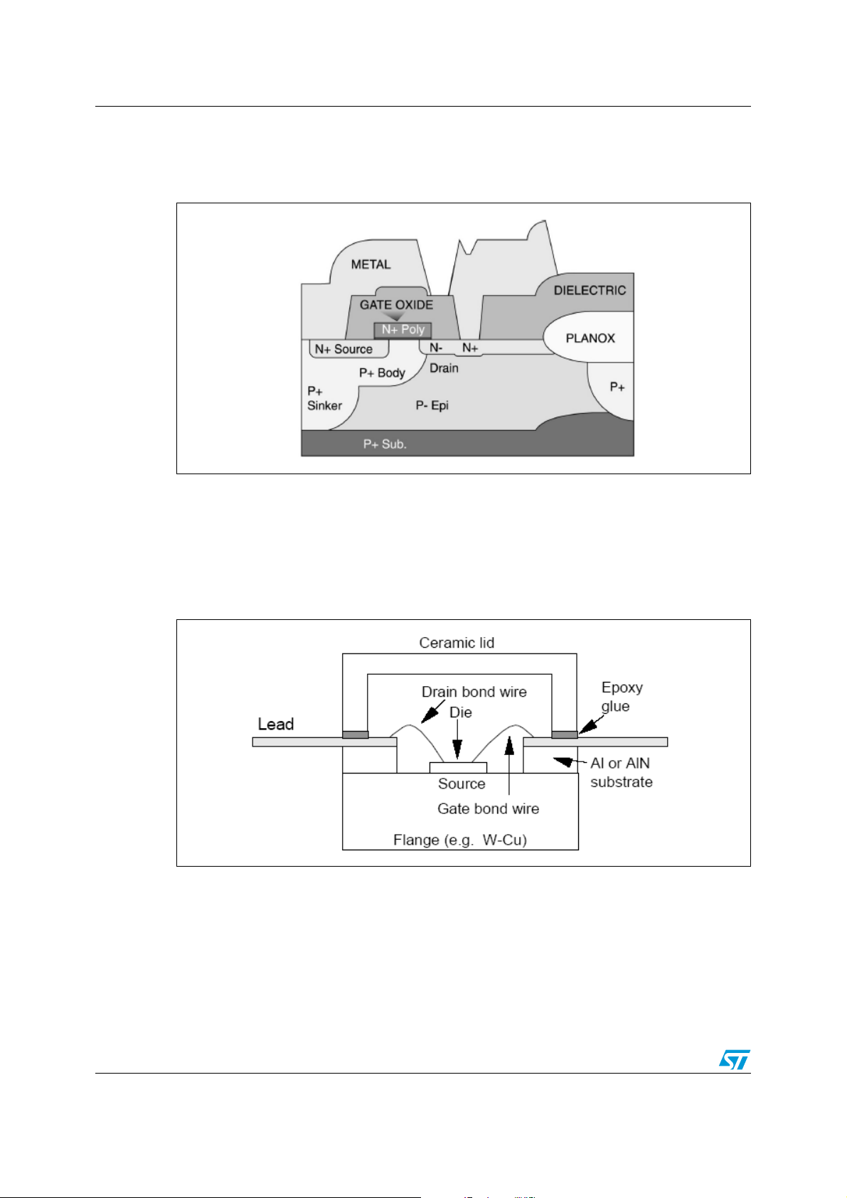
Figure 1. LDMOS cross section
In such a structure there is no need to electrically isolate the die from the flange as for
bipolar die, by using a Beryllium Oxide (BeO) interface (Figure 1 and Figure 2). LDMOS
package development eliminates any substances which could affect and/or deteriorate the
environment. Because BeO is toxic, it is no longer used. The LDMOS die is soldered directly
to the flange (for example, the tungsten-copper alloy flange) which results in better electrical
and thermal performances.
Figure 2. LDMOS package structure
2/6
Page 3

AN1233 Mounting techniques and characteristics
2 Mounting techniques and characteristics
Surface mount packages were developed to reduce assembly cost and space allocation on
printed circuit board (PCB). Today, ST microelectronics offers three types of packages for its
L-DMOS product: Flange, Flangeless and SMD (Figure 3). All three package types have
their own mounting techniques and characteristics.
Figure 3. Package styles
2.1 Flange package (e.g. M243 package)
Heatsink flatness on the mounting area must be better than 0.02 mm. The mounting area
roughness must be less than 0.5 µm. Flux solution is not needed. Because the package is
non hermetically sealed, damage could occure. The PCB must be thoroughly washed clear
of flux solution before mounting the RF transistor. Then a thin layer of thermal paste must be
applied to the flange; however, an excessive thickness of thermal paste increases the
thermal resistance and caution must be used. Screws with a flat washer must be used in
order to apply pressure evenly on the joints. Each screw must be slightly tightened (finger
tight: 0.05 Nm) and then the screws must be tightened to the specified torque. A typical
torque value for M243 package is 0.65 Nm.
Reflow soldering is the recommended mounting technique even though clamping can also
be used. The backside of the package must be directly soldered to the heatsink. (See
Figure 4 for the flangeless package).
3/6
Page 4

Mounting techniques and characteristics AN1233
Figure 4. Flangeless package mounting
2.2 Flangeless package (e.g. M250 package)
Reflow soldering is the recommended mounting technique even though the clamping
method can also be used. The backside of the package must be directly soldered to the
heatsink (see Figure 4).
2.3 SMD package (e.g. SO-8 ceramic)
Reflow soldering is the recommended mounting technique. Clamping can also be used.
Dissipated power (heat) is mainly transferred by conduction from the device to the heatsink
through the printed circuit board.
Thermal resistance from the junction to the ambient must be reduced to a minimum value,
hence all interfaces between the package and the ambient must be taken carefully into
consideration (see Figure 5). Metallized ground plate and leads contribute to the heat flow. It
is recommended to mount the device on a large grounded metallized area on the printed
circuit board. Since the PCB is a poor thermal conductor (FR4, Duroid, etc.), it is also
recommended to use thermal vias (plated through holes) to improve heat conduction.
Figure 5. SMD package mounting
4/6
Page 5

AN1233 Lowering the thermal resistance between junction and ambient
3 Lowering the thermal resistance between junction
and ambient
In order to decrease the thermal resistance between the junction and the ambient, the
following actions may be considered:
1. Increase the number of plated through holes.
2. Increase the holes diameter. However, it must be kept in mind that if the diameter is too
large, solder leaks out and forms solder balls beneath the PCB. This increases the
thermal resistance between PCB and heatsink (0.5 mm < Hole diameter < 1.0 mm).
3. Decrease spacing between plated through holes.
4. Decrease thickness of the printed circuit board.
5. Use of a thin layer of thermal paste between PCB and heatsink.
6. Screw the PCB to the heatsink as close as possible to the package. The screws also
help heat to flow to the heatsink (see Figure 5).
4 Revision history
Table 1. Revision history
Date Revision Changes
05-Oct-2006 2 Minor text changes
30-Jul-2007 3 The document has been reformatted
5/6
Page 6

AN1233
Please Read Carefully:
Information in this document is provided solely in connection with ST products. STMicroelectronics NV and its subsidiaries (“ST”) reserve the
right to make changes, corrections, modifications or improvements, to this document, and the products and services described herein at any
time, without notice.
All ST products are sold pursuant to ST’s terms and conditions of sale.
Purchasers are solely responsible for the choice, selection and use of the ST products and services described herein, and ST assumes no
liability whatsoever relating to the choice, selection or use of the ST products and services described herein.
No license, express or implied, by estoppel or otherwise, to any intellectual property rights is granted under this document. If any part of this
document refers to any third party products or services it shall not be deemed a license grant by ST for the use of such third party products
or services, or any intellectual property contained therein or considered as a warranty covering the use in any manner whatsoever of such
third party products or services or any intellectual property contained therein.
UNLESS OTHERWISE SET FORTH IN ST’S TERMS AND CONDITIONS OF SALE ST DISCLAIMS ANY EXPRESS OR IMPLIED
WARRANTY WITH RESPECT TO THE USE AND/OR SALE OF ST PRODUCTS INCLUDING WITHOUT LIMITATION IMPLIED
WARRANTIES OF MERCHANTABILITY, FITNESS FOR A PARTICULAR PURPOSE (AND THEIR EQUIVALENTS UNDER THE LAWS
OF ANY JURISDICTION), OR INFRINGEMENT OF ANY PATENT, COPYRIGHT OR OTHER INTELLECTUAL PROPERTY RIGHT.
UNLESS EXPRESSLY APPROVED IN WRITING BY AN AUTHORIZED ST REPRESENTATIVE, ST PRODUCTS ARE NOT
RECOMMENDED, AUTHORIZED OR WARRANTED FOR USE IN MILITARY, AIR CRAFT, SPACE, LIFE SAVING, OR LIFE SUSTAINING
APPLICATIONS, NOR IN PRODUCTS OR SYSTEMS WHERE FAILURE OR MALFUNCTION MAY RESULT IN PERSONAL INJURY,
DEATH, OR SEVERE PROPERTY OR ENVIRONMENTAL DAMAGE. ST PRODUCTS WHICH ARE NOT SPECIFIED AS "AUTOMOTIVE
GRADE" MAY ONLY BE USED IN AUTOMOTIVE APPLICATIONS AT USER’S OWN RISK.
Resale of ST products with provisions different from the statements and/or technical features set forth in this document shall immediately void
any warranty granted by ST for the ST product or service described herein and shall not create or extend in any manner whatsoever, any
liability of ST.
ST and the ST logo are trademarks or registered trademarks of ST in various countries.
Information in this document supersedes and replaces all information previously supplied.
The ST logo is a registered trademark of STMicroelectronics. All other names are the property of their respective owners.
© 2007 STMicroelectronics - All rights reserved
STMicroelectronics group of companies
Australia - Belgium - Brazil - Canada - China - Czech Republic - Finland - France - Germany - Hong Kong - India - Israel - Italy - Japan -
Malaysia - Malta - Morocco - Singapore - Spain - Sweden - Switzerland - United Kingdom - United States of America
www.st.com
6/6
 Loading...