

Page 1
AN1232
Application note
Ruggedness improvement
of RF DMOS devices
Introduction
RF amplifiers often experience impedance mismatch between output and load. Such an
impedance mismatch generates a reflected wave towards the RF power transistor, making a
much more stringent working environment for the transistor. Working conditions grow critical
when the load is disconnected from the output of the RF power transistor, since, in this case,
the reflected wave amplitude becomes comparable to the incident one.
RF transistors are able to withstand severe impedance mismatch conditions particularly
essential for applications such as plasma generators or nuclear magnetic resonators which
operate under rough conditions. DMOS devices used in such applications appeared to lack
the necessary ruggedness when operating under severe RF load mismatch conditions. This
weakness was believed to be intrinsic.
Based on the need to improve the ruggedness of RF power DMOS, an investigation was
carried out and a theoretical model simulating the failure mode mechanism was developed.
Finally, relevant corrective actions were undertaken.
July 2007 Rev 13 1/6
www.st.com
Page 2
Proposed model AN1232
1 Proposed model
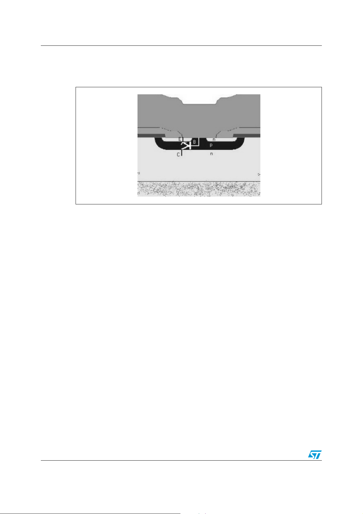
Figure 1. Npn Bipolar parasitic transistor
Under impedance mismatch conditions the RF power transistor is subjected to a reflected
wave with an amplitude that cannot be controlled and, in the worse case, with a voltage
value that can exceed the BV
clamp for this wave. Under such conditions the device is subjected to an electric current
whose amplitude is proportional to the power of the incident wave. Simultaneously, the
DMOS experiences a temperature rise proportional to the duration, voltage swing (BV
and amplitude of the above current. In the DMOS cross section, shown in Figure 1, the
presence of an npn bipolar parasitic transistor, in which the base and emitter are shorted by
means of the DMOS source metallization, are clearly noticeable.
of the device itself. Hence, the DMOS works as a voltage
dss
dss
)
Under static conditions the parasitic transistor is inhibited by the short circuit, but under
dynamic conditions, when the reverse breakdown current flows through the device, the short
circuit condition itself is modified. In fact, this current crosses the base-emitter junction
through the base resistance which is increased by the depletion layer due to the reverse
voltage. This results in a variation in V
be
We can assume that:
Equation 1
V
If I
(base distributed current) and Rbe (base distributed resistance) are large enough, the
dis
potential on the emitter side opposed to the short circuit is sufficient to turn on the bipolar
transistor, thus concentrating the current and destroying the device.
A simplified model was developed (see Figure 2) to simulate the mismatch condition on the
drain of the DMOS by means of the inductance L.
2/6
be
.
RbeI
•=
dis
Page 3

AN1232 Proposed model
Figure 2. Mismatch condition model
During the turnoff period the device is in breakdown condition and subjected to the current
induced by the inductance, thus the device dissipates power. Of course, depending on the
turnoff duration, we have to distinguish between the turn-on of the parasitic transistor and
the thermal derating, with relevant operations out of the reverse safe operating area of the
DMOS. In fact, during such operations it is possible that the device exceeds the maximum
allowed junction temperature (200 °C). In the case of load mismatch, however, the value of
the inductance is far from causing a thermal overstress. Therefore, a turn-on due to R
be
is
far more likely to happen.
Another occurrence is when the voltage, due to the reflected wave, is applied on the drain of
the DMOS at zero current. In this case the capacitance of the body-drain junction is
involved. This capacitance suddenly changes value due to the changed potential, hence
making a current whose value is given by:
Equation 2
dV
I
dis
-------
C
•=
bd
dt
this together with Equation 1 gives:
Equation 3
dV
RbeC
V
be
bd
-------
••=
dt
Therefore, one can see that even a zero current switching condition can cause the turn-on of
the parasitic transistor.
3/6
Page 4

Actions AN1232
2 Actions
In order to validate the model several tests were performed. The failure current was
measured during a UIS (Unclamped Inductive Switching) test. In particular the failure
current density was also tested. Results are listed in Ta bl e 1 .
In a typical DMOS structure the body acts as the base of the parasitic transistor while the
source behaves as the emitter. The R
using the existing diffusion processes it is not possible to change the body doping value in
order to reduce either the DC gain (h
DMOS threshold voltage. The only way to work on the parasitic transistor, without changing
the characteristics of the DMOS, is to add a further doping level called deep-body doping.
By doing so the R
pinched is dramatically reduced to 100 ohm/square and the DC gain (hfe)
s
of the parasitic transistor becomes close to one. This extra doping is implanted following the
body doping process and prior to the body diffusion process. The Dmos structure is
therefore modified as shown in Figure 3.
Figure 3. Deep body doping
pinched values are typically in the KWs range. By
s
) or the Rbe. This would have a dramatic impact on the
fe
Since the deep body process is separated from the main body process (a further masking
level and implant are required), typical DMOS parameters are unaffected. Optimum values
for UIS and in VSWR can be obtained by using this structure and varying the deep body
implant doses. Results from the test performed on the SD2921 device are listed in Ta bl e 1 .
Table 1. UIS and VSWR output mismatch vs deep body dose
Deep body dose UIS Failure (A) VSWR
None 10 5:1
1e15 26 15:1
2e15 39 20:1
3e15 45 30:1
4/6
Page 5

AN1232 Conclusion
3 Conclusion
We have demonstrated that DMOS ruggedness, under varying load mismatches, is
dramatically improved with a single implant process through photoresist without modifying
the DMOS layout. Also, RF power performances remain unaffected. From now on, deep
body doping process will be applied to all products in the production phase.
VSWR, a characteristic ruggedness parameter for RF power transistors, is linked to the
standard ruggedness parameters of the DMOS. Therefore, a UIS test, easily implemented
and commonly applied in EWS (Electrical Wafer Sort), can give useful information on the
ruggedness of RF power devices.
4 Revision history
Table 2. Revision history
Date Revision Changes
21-Jun-2004 12 Minor text changes
30-Jul-2007 13 The document has been reformatted
5/6
Page 6

AN1232
Please Read Carefully:
Information in this document is provided solely in connection with ST products. STMicroelectronics NV and its subsidiaries (“ST”) reserve the
right to make changes, corrections, modifications or improvements, to this document, and the products and services described herein at any
time, without notice.
All ST products are sold pursuant to ST’s terms and conditions of sale.
Purchasers are solely responsible for the choice, selection and use of the ST products and services described herein, and ST assumes no
liability whatsoever relating to the choice, selection or use of the ST products and services described herein.
No license, express or implied, by estoppel or otherwise, to any intellectual property rights is granted under this document. If any part of this
document refers to any third party products or services it shall not be deemed a license grant by ST for the use of such third party products
or services, or any intellectual property contained therein or considered as a warranty covering the use in any manner whatsoever of such
third party products or services or any intellectual property contained therein.
UNLESS OTHERWISE SET FORTH IN ST’S TERMS AND CONDITIONS OF SALE ST DISCLAIMS ANY EXPRESS OR IMPLIED
WARRANTY WITH RESPECT TO THE USE AND/OR SALE OF ST PRODUCTS INCLUDING WITHOUT LIMITATION IMPLIED
WARRANTIES OF MERCHANTABILITY, FITNESS FOR A PARTICULAR PURPOSE (AND THEIR EQUIVALENTS UNDER THE LAWS
OF ANY JURISDICTION), OR INFRINGEMENT OF ANY PATENT, COPYRIGHT OR OTHER INTELLECTUAL PROPERTY RIGHT.
UNLESS EXPRESSLY APPROVED IN WRITING BY AN AUTHORIZED ST REPRESENTATIVE, ST PRODUCTS ARE NOT
RECOMMENDED, AUTHORIZED OR WARRANTED FOR USE IN MILITARY, AIR CRAFT, SPACE, LIFE SAVING, OR LIFE SUSTAINING
APPLICATIONS, NOR IN PRODUCTS OR SYSTEMS WHERE FAILURE OR MALFUNCTION MAY RESULT IN PERSONAL INJURY,
DEATH, OR SEVERE PROPERTY OR ENVIRONMENTAL DAMAGE. ST PRODUCTS WHICH ARE NOT SPECIFIED AS "AUTOMOTIVE
GRADE" MAY ONLY BE USED IN AUTOMOTIVE APPLICATIONS AT USER’S OWN RISK.
Resale of ST products with provisions different from the statements and/or technical features set forth in this document shall immediately void
any warranty granted by ST for the ST product or service described herein and shall not create or extend in any manner whatsoever, any
liability of ST.
ST and the ST logo are trademarks or registered trademarks of ST in various countries.
Information in this document supersedes and replaces all information previously supplied.
The ST logo is a registered trademark of STMicroelectronics. All other names are the property of their respective owners.
© 2007 STMicroelectronics - All rights reserved
STMicroelectronics group of companies
Australia - Belgium - Brazil - Canada - China - Czech Republic - Finland - France - Germany - Hong Kong - India - Israel - Italy - Japan -
Malaysia - Malta - Morocco - Singapore - Spain - Sweden - Switzerland - United Kingdom - United States of America
www.st.com
6/6
 Loading...