

Page 1
AN1230
APPLICATION NOTE
LNB SUPPLY AND CONTROL VOLTAGE REGULATOR
(PARALLEL INTERFACE)
F. Lentini - G. Benenati
1. ABSTRACT
LNBP is the integrated solution for supplying/interfacing satellite LNB modules. It gives good
performances in a simple and economical way, with a minimum use of external components. It is
comprised of functions that realize LNB supplying/interfacing in accordance to the international
standards.
2. INTRODUCTION.
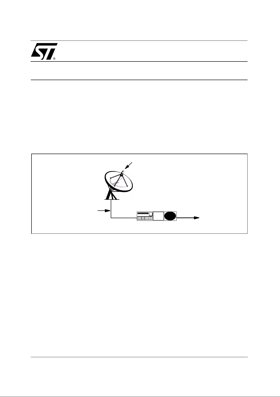
Figure 1: Basic Satellite Installation
LNB
Parabola
Coaxial
Cable
Satellite
To TV Set
Receiver
A typical satellite receiver system is formed by these blocks (reported in figure 1):
1. The parabola is the antenna of the system and focus es the sate llite s ignal to the LNB ;
2. The LNB (low noise block ) is placed on the focus of the parabola an d converts the incoming
signal in the 10GHz range to a lower frequency signal (in the 1-2GHz range) called "first
conversion signal". Th is a llows th e sig nal to be c arried b y an in expens ive c oaxial cable t owards
the receiver. Additionally, it improves the first conversion signal level by a built-in low noise
amplifier. A universal LNB can change the type of polarization (horizontal or vertical) or operative
band by command signals sent by the receiver;
3. The coaxial cable joins the LNB to the receiver and carries out 3 functions:
a) to transfer the first conversion signal from the LNB to the receiver;
b) to transfer the command signal s from t he receiver to th e LNB to change polarization or signal
band;
c) to carry the DC voltage to supply the LNB.
4. The receiver converts the first conversion signal into control signals for the TV system. The
receiver provides for that provides for two important features:
July 2000
1/17
Page 2
AN1230 - APPLICATION NOTE
a) to supply the LNB block;
b) to generate all the signals/voltages that LNB needs to operate correctly.
5. The supply/interface block is placed inside the receiver . It must perform the following functions:
a) be ready to accept future digital standards with an external modulation
input and fast oscillator
start-up;
b) implement the loop-through function in slave condition for single dish, multiple receiver
system;
c) accept the paralleling of 2 or more receivers and, in this condition. av oid the flow of reverse
current from the output to the GND;
d) give accurate, thermal compensated outputs with the possibility to compensate the DC
voltage drop caused by long coaxial cables;
e) be reliable;
f) provide overload (better if dynamic) and thermal protection with diagnostic;
g) avoid every type of trimming;
h) provide the possibility to be driven by a microcontroller or a simple digital logic to implement all
these functions;
i) Finally, it must be cheap and get a small area in the board.
All these functions are hard to be implemented with discrete components, but are greatly made easier by
using an integrated device, like LNBP, that has been specially designed for this purpose.
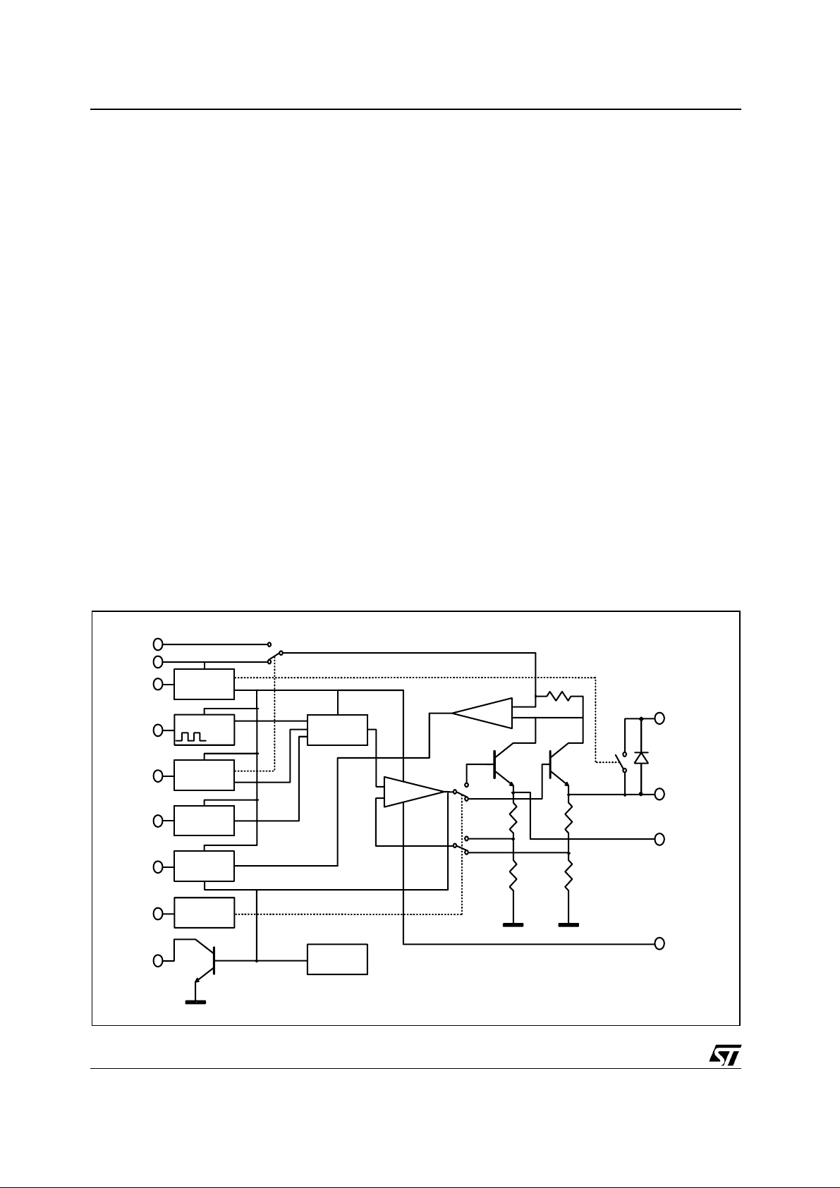
3. FUNCTIONAL BLOCKS.
LNBP comprises the following operative blocks (see figure 2):
Figure 2: Internal Block Diagram
Vcc1
Vc c 2
EN
ENT
VSE L
LLC
CE XT
OS EL
OL F
PRE RE G.
OSCI LLATO R
22KHz
OUT PUT VOLT
SELECTION
LINE LENGHT
COMPE NSAT ION
CURRENT LIMIT
OUT PUT POR T
SELECTION
REFERENCE
ERR.AMP.
THERMAL PROT.
CURR.AMP.
MI
LNBA
LNBB
EXTM
2/17
Page 3
AN1230 - APPLICATION NOTE
1. The oscillator is act ivated by putting t he ENT pin (En able Tone) = H and is factory trimmed at
22KHz ± 2KHz, avoiding the need to use external trimming. The rise and fall edges are
controlled to be in the 5 to 15µs range, 10µs typ., to avoid RF pollution towards the receiver. The
Duty Cycle is 50% typ. It modulates the DC output with a ± 0.3V amplitude and 0V average. The
presence of this signal usually gives the LNB information about the band to be received.
2. The OSEL (OUTP U T POR T SELECTION) selects the two outputs of the LNB (LNBA and LNBB),
in order to drive a dual-dish system, depending o n its present state. When O SEL i s L, the L NBA
port is selected. When OSEL is H, the LNBB port is selected. The LNBA and LNBB outputs
supply either 13V or 18V. If VSEL is low (VSEL = L) 13V is selected, otherwise, if VSEL is high
(VSEL = H) 18V is sel ected. This kind of feature chan ges the LNBP polarization type. The LNB
switches horizontal or vertical polarization depending on the supply voltage it gets from the
receiver.
3. In order to keep the power dissipation of the device low, the input selector automatically selects
Vcc1, that is the lowest input voltage, when 13 V out is selected (i.e. VSEL is L). If 18V out is
selected (i.e. VSEL is H), Vcc2 input is selected. So power dissipation at Iout=500mA is:
Pd=(22-18)*0.5=2W (with Vcc2=22V and Vout=18V) or (15-13)*0.5=1W (with Vcc1=15V and
Vout=13V). Without input selection we should have Pd=(22-13)*0.5=4.5W, which is much higher.
Moreover, an internal switch selects the MI (MASTER INPUT) to be transferred to the LNBA
when the EN pin is low. This case occurs when two receivers are connected in series and the
slave receiver (the nearest to the antenna) is disabled. The master receiver supplies the LNB by
means of the MI input of the slave receiver .
4. The line length compensation f unction is us eful when the antenna is connected to t he rec eiver
by a long coaxial cable that adds a considerabl e DC voltage drop. When the LCC pin is H, the
output voltage selected is increased by about 1V.
5. The reference drives all the internal blocks that require a high precision thermal compensated
voltage source.
6. The LNBP has two different protection features, and both turn off the outp uts. The first one a cts
in overload conditions (i.e. for output current ≥ 500mA), and the s econd f or overheating (i.e. for
Tamb ≥ 150°C).
a) The overload protection case occurs when output current request is ≥ 500mA. In this condition
the device limits the output current at 500mA for a time Ton dep ending on the Cext value.
When Ton has elapsed, output goes low for a time of Toff=15*Ton. This keeps the power
dissipated by the device low in overload conditions, and avoids to ov ersize the heatsink in
such a condition.
b) In the thermal protection case the output is disabled until the chip temperature has fallen. After
that the LNBP restarts working properly. The LNBA bypass switch is not protected, so the MI
input must be driven by a current limited voltage source.
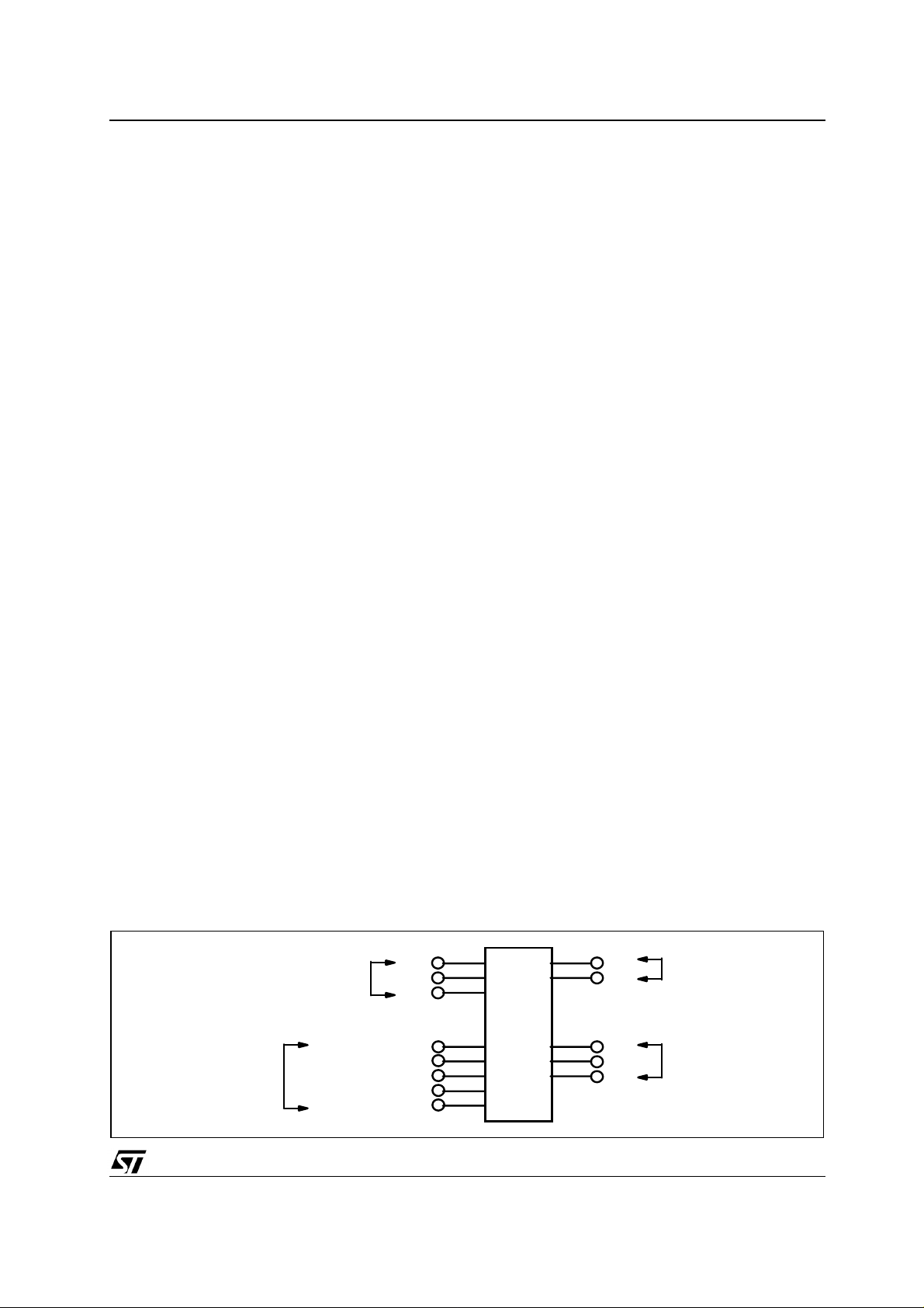
Figure 3: LNBP Pin Grouping
INPUTS
CONTROL
SIGNAL
OSEL (L=LNBA, H=LNBB)
MI
Vcc2
Vcc1
EN (ACTIVE H)
LLC (ACTIVE H)
ENT (ACTIVE H)
VSEL (L=13V, H=18 V)
LNBP20CR
LNBA
LNBB
EXTM
CEXT
OLF
OUTPUTS
3/17
Page 4
AN1230 - APPLICATION NOTE
In figure 3 the LNBP pins are grouped by functions. The 5 control signals are logic inputs that control the
IC function, and it is recommended that the VIH not exceed 7V .
Cext controls the res tore timing of the overload protection. If an overload protection is p resent, output
goes low for a time imposed by the Cext value. At the same time the OLF pin, an open collector output,
goes low.
In figure 4 and figure 5 the behav ior o f Ton and Toff times vs. Cext is respectively shown. When Toff has
elapsed, the output retu rns ac tive f or a time Ton=Toff/1 5. The n, OLF returns a hig h im ped anc e ou tpu t. If
the overload is still present the cycle is repeated. This behavior greatly reduces the dissipation in the
device. In fact, in short circuit conditions with Vcc2=25 V, considering Iout internally limited at 650mA and
Toff=15*Ton we obtain: Pd average=V in*Iout*Ton/(Ton+Toff)=2 5*0. 65*1/(1+15)=1.02W, that is lower than
the power dissipated in normal conditions.
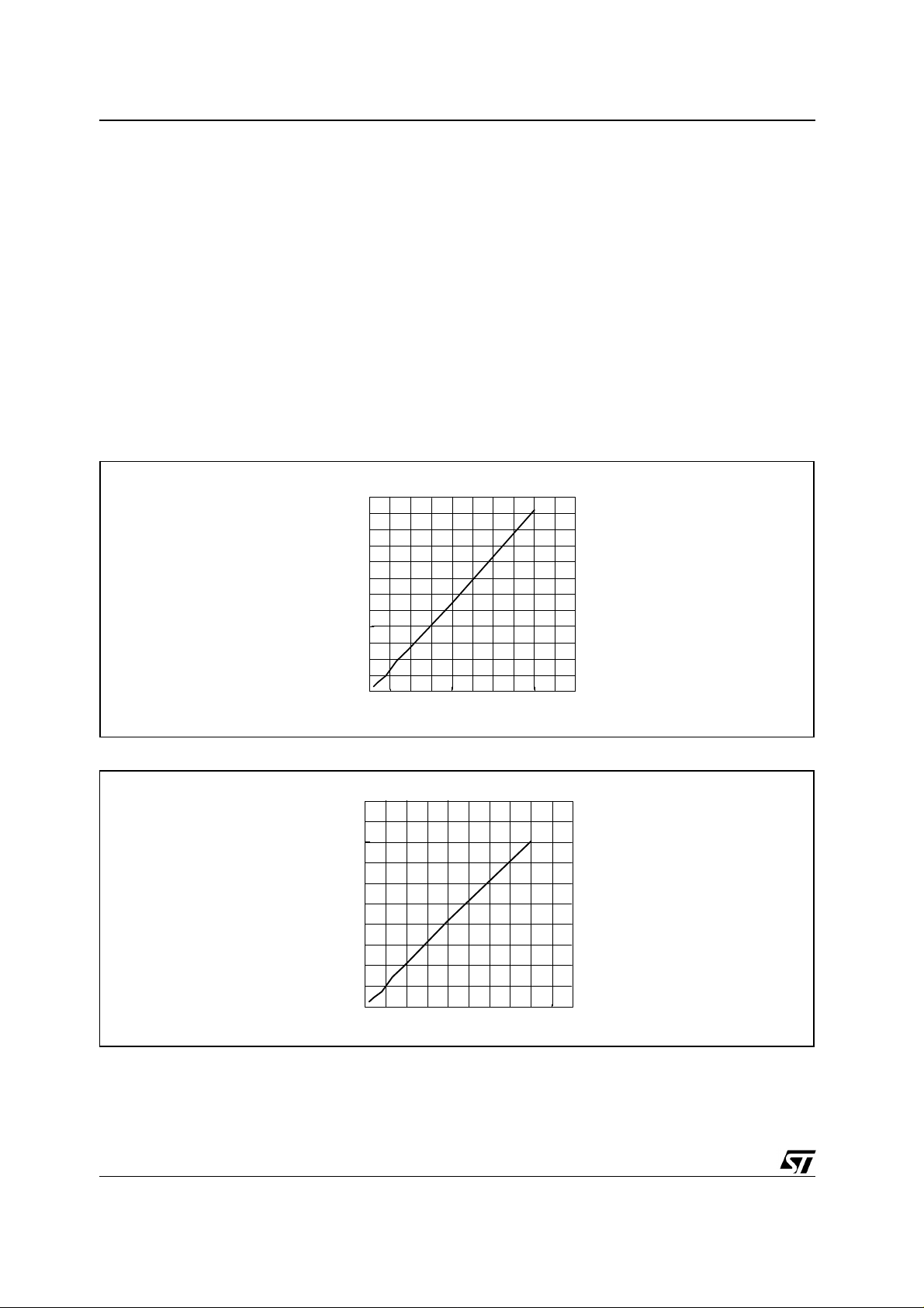
Figure 4: Overload Protection On Time versus C
Ton time vs. Cext
300
250
200
150
ton (ms)
100
50
0
0 5 10 15 20 25
CAPACIT OR Cext ( µF )
Figure 5: Overload Protection Off Time versus C
T off time vs. Cext
5,000
4,000
3,000
ext
ext
toff (ms)
2,000
1,000
0
0 5 10 15 20 25
CAPACI T OR Cext ( µF )
The Cext must be properly chosen. It is related to the Iout and Cout (total capacitor connected to the
LNBA or LNBB output) values. Large Cout values at start-up give high current peak for a long time, and
consequently, an overload condition for a time that could be great er than the Ton imposed by Cext. So
the output will be forced low, completely discharge and will not start. For proper use it is neces sary that
4/17
Page 5
AN1230 - APPLICATION NOTE
Cout/Cext ≤ 20. The OLF also gives information about the thermal protection status. If the thermal
protection is triggered, the output is disabled and the OLF goes low. When the chip temperature has
fallen, the output returns active and the OLF returns to its 3-state condition.
By sensing the O N/OFF ratio of the OLF signal, a microcontroller can discrimina te if an overload or a
thermal protection is present.
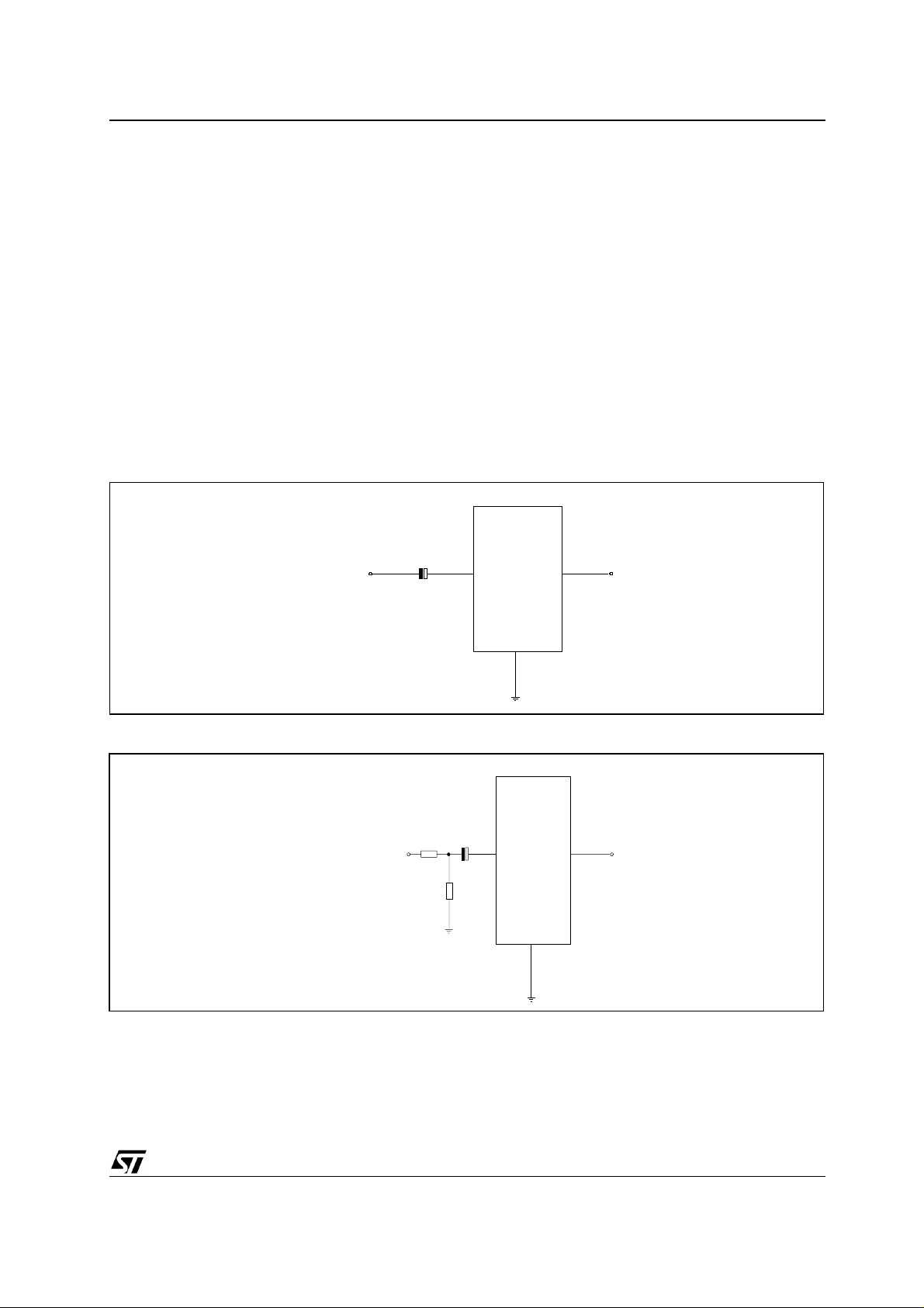
EXTM modulates the Vout by a capacitor connected in series (see figure 6). In this case:
Vout a.c.=Vin a .c.*Vout d.c./3 where, respectively, Vout a.c. and Vin a.c. are alternate components of
Vout and Vin, and Vout d.c. is the direct com ponent of Vout. For example, if an a.c. signal of 600mV p.p.
must be imposed to the 13V d.c. out, the formula is as follows:
Vin a.c.= 3*Vout a.c./Vout d.c.=3*600/13 ª140 mV p.p. If we dispose a 0-5V square wave signal to
modulate output voltage, it is necessary to lower this signal amplitude. In accordance to figure 7 we have:
R1=R2*(V1/Vin-1).
Figure 6: How t o Us e EX T M In pu t
External
Modulation
Input
Vin
Cin = 10µF
EXTM
LNBP
Figure 7: How to Adjust the External Modulation Level
External
Modulation
Input
Cin = 10µF
R1
V1
R2
Vin
LNBA
or
LNBB
EXTM
LNBP
LNBA
or
LNBB
Vout
Vout
R2 must be i n the 50Ohm rang e to minimize the effects of the EX TM input resistance variat ions. In our
example we obtain:
R1=50*(5/0.14-1)=1.7kOhm.
As a side effect, the EXTM modifies the Vout by a resistor connected between this input and the GND.
Figure 8 and 9 report the Vout value vs. R.
5/17
Page 6
AN1230 - APPLICATION NOTE
Figure 8: Vout Value vs. Resistance on the EXTM pin at VSEL = L
Vout value vs. Resistance
15.00
14.50
Vcc1= Vcc2 = 24V
14.00
13.50
13.00
12.50
OUTPUT VO LTAGE (V)
12.00
10K 4.7K
∞
2.2K
Resistance (Ohm)
Ta=+25°C
1K1.5K 680 470 330 220 150 100 47 0
Figure 9: Vout Value vs. Resistance on the EXTM pin at VSEL = H
Vout value vs. Resistance
20.50
20.00
Vcc1= Vcc2 = 24V
19.50
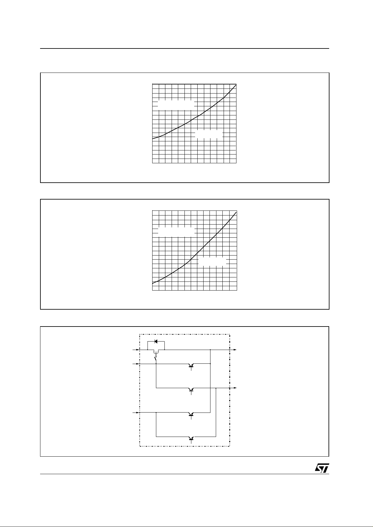
Figure 10: LNBP Output Stages
MI
Vcc2
22V TO 25V
Vcc1
15V TO 25V
19.00
18.50
18.00
OUTPUT VOLTAGE (V)
17.50
10K 4.7K2.2K 1K1.5K 680 470 330 220 150 100 47 0
∞
Ta=+25°C
Resistance (Ohm)
D
SW1
TR1
S
G
TR2
TR3
LNBA
13V OR 18V
LNBB
13V OR 18V
TR4
6/17
TR5
Page 7

AN1230 - APPLICATION NOTE
4. OPERATING MODE.
LNBP has 3 power inputs (Vcc1, Vcc2 and MI) and two outputs (LNBA, LNBB) internally connected
in accordance to the scheme reported in figure 10. By analyzing this scheme we can make out
the following results:
1. TR1 is an N-channel Power MOSFET with its source connected to the LNBA. It is driven by SW1,
that joins the gate to Vcc2. The drop between MI and LNB A is due to the Ron of TR1, but in
some conditions it is increased by inadequate driving. In fact we have:
Vdrop=Vdrain-Vsource=VMI-(Vcc2-Vgs)=Vgs-(Vcc2-VMI).
We can see that the drop can be minimized increasing the (Vcc2-VM I) value. For example, if
Vcc2 increases, the effect of inadequate driving is cancelled.
Vgs depends on the T R1 and Iout characteristics. Figure 11 gives the Vgs vs. Iout plot, with
Vcc2-VMI as the paramet er. Therefore, given Iout,Vcc2 and VMI w e can c alculate t he Vdrop. If
Vcc2=22V, MI=21V and Iout=500mA the formula is as follows: Vdrop=Vgs-1V. In figure 11 it
results that Vgs=3.1V at ILOAD=500mA and Vcc2-VMI=1V and in such conditions
Vdrop=3.1V-1V=2.1V.
If we increase Vcc2 at 26V we obtain: Vdrop=5.65V-5V=0.65V, which is much lower.
Figure 11: Loop-Through Switch Gate Voltage
Vgs vs. Iout
5.5
6
Figure 10
V cc2 -V MI = 5 V
5
4.5
Vgs (V)
3.5
2.5
V cc2 -V MI = 4 V
4
V cc2 -V MI = 3 V
3
Vcc2 - VMI = 1
2
0 100 200 300 400 500 600 700
Iout (mA)
÷
2V
2. In some cases it happens that two or more receivers share the s ame coaxial cable making their
output hard paralleled, so the same voltage is present at the outputs of the receivers. If a
receiver is not disconnected at the mains, it will flow a current from the LNBA to the MI by means
of the parasitic D-S TR1 diode. Moreover, the TR2 (or TR4) B
could be exceeded, so a
Vb-e
reverse current could flow from the LNBA to Vcc2 (or Vcc1) or from the LNBB to Vcc2 (or Vcc1),
with possible destruction of the relative transistor. To overcome this drawback it is enough to add
one or two diodes, depen ding on how many outputs are used, in series at the LNBA or LNBB
pins (see figure 12). In this case we have to consider th e voltage drop across the diode that is
load and temperature depende nt. These e ffects can be minimized by using Schott ky di odes and
activating the LLC function.
In alternative we can add one, two or three diodes - it depends if one, two or three inputs are used - in
series at input oins M1, Vcc1 and Vcc2 (see figure 13). In this case diodes do not causea change at Vout,
but only a worsening of voltage drop, that can be minimized by us ing Shottky diodes. Diodes used in
figures 12 and 13 must withstand a continuous current of a lmost 1A and a breakdown voltage of 30V
(suggested type is BYV10-30).
7/17
Page 8

AN1230 - APPLICATION NOTE
Figure 12: Reverse Current Protection Using Diodes on the Outputs
MI
Vcc2
Vcc1
LNBP
LNBA
LNBB
LNBA’
LNBB’
Figure 13: Reverse Current Protection Using Diodes on the Inputs
MI’
Vcc2’
Vcc1’
MI
Vcc2
Vcc1
LNBA
LNBP
LNBB
3. In alternative we can add one, two or three dio des, depending on h ow many inputs are used, in
series at the MI, Vcc1 and Vcc2 input pins (see figure 13). In this case diodes do not cause a
change at Vout, but only worsen the voltage drop, which can be minimized by using Schottky
diodes. Diodes used in figures 12 and 13 must withstand a continuos current of almost 1A and a
breakdown voltage of 30V (suggested type is BYV10-30).
5. APPLICATION HINTS.
1. LNBP has an LLC pin to compens ate the voltage drop across the cable. This pin ad ds a discrete
1V value at the selected output voltage when it is active. It is also possible to obtain a continuous
variation of the LNBA or LNBB voltage by using EXTM input.
2. If only a single 22V source is su itable, at the cost of higher power losses in the device and higher
heatsink surface, it is possible to power the Vcc1 and Vcc2 pins by the same 22V source without
affecting any other circuit performance. In order t o reduce power dissipation in the device, it can
be useful to insert an adequate resistor in series to the V cc1 pin (see figure14). This resistor
must be dimensioned considering that the minimum voltage on the Vcc1 pin must be ≥ 16 V, with
a supply current I
SUPPLY
= 500 mA.
This means: R ≤ (22-16) / 500 *10 -3 ≅ 12 Ohm.
Power dissipated in this resistor is:
Pd = R*Iout
2
= 12* (500*10 -3)2 = 3W.
It is recommended to bypass the Vcc1 and Vcc2 pins by 2.2µF electrolytic capacitors.
3W is the power dissipated saved by the device.
3. If Vcc2 is not inserted (i.e. the receiver is not connected to the mains) the TR1 can not bypass MI
to the LNBA, because the gate is not driven (see figure 10). It is possible to overcome this
drawback by using the scheme reported in figure 15.
8/17
Page 9

Figure 14: How to Get Vcc1 Using a Drop Resistor
AN1230 - APPLICATION NOTE
VIN
MI
VCC2
LNBP
VCC1
LNBA
LNBB
Figure 15: A Lo op-Throu gh Switch Th at Work s Wit ho ut Vc c 2
MI
VCC2
LNBP
VCC1
6. SINGLE SUPPLY APPLICATION.
In some applications (TV receivers, PC cards, et c.) a 12 V power s uppl y is availa ble. It is po ssible to use
this voltage to supply the LNBP. Figure 16 reports the schema tic of the application proposed. It uses an
MC34063 to step-up the 12V input at a value of 16V or 23V, depe nding on the Vsel status. If Vsel is H
(i.e. the LNBP gives 18V at out LNBA), a 23V voltage is available at point A. If Vsel is L (i.e. the LNBP
gives 13V at out LNBA), a 16V vol tage is a vailable at poin t A. Th is keeps the power dissipated by LNBP
low and gives good efficiency because the LNBP is supplied with a minimum drop. Diode D2 protects the
LNBP by reverse current. If the LNBP is disabled (i.e. En is L), the 23V voltage is selected at point A,
regardless of the Vsel status. The changing voltage at point A is actuated by HC03, which is an
open-drain quad 2-input nand gate.
Figure 16: Single Supply Application Using MC34063A Plus LNBPxx
BYV10-40
R3
47K
R4
2.7K
HC03
R5
1.2K
+
C3
330uF
HC03
R6
10KR710K
HC03
A
C4
.22uF
4.7uF
C6
+
+Vin
12V
+
C1
100uF
R1
0R15
0.5W
150uH
R2
100R
1W
7
6
4
2
MC34063
8
1
5
3
C2
1nF
1N4007
Vcc1
LNBA
Vcc2
Cext
LNBP
VSel
MI
En
C5
10nF
BYV10-40
LNBA
13/18
V
MI
VSel
En
+5V
9/17
Page 10

AN1230 - APPLICATION NOTE
7. DiSEqC* SPECIFICATION.
Figure 17: Im p e dance Match i ng f or DiSEqC
R1
LNBP
ENT
OUT
LNBA
or
LNBB
15Ω
BUS
L1
270µH
DiSEqC
IN
The DiSEqC standard was born to implement the most complex system required, for example, by
multiple-satellite installations, where multiple LNB placed in the parabola must communicate with the
receiver in a two-way mode. This standard is compatible with 13/18V and 22kHz tone and is easily
implemented by a microcontroller. It requires hardware specifications that are faithfully satisfied by LNBP.
In particular, the bus impedan ce can be matched using the scheme reported in figure 17.
8. THERMAL MANAGEMENT.
Figure 18: Thermal Resistance versus On-Board Copper Heatsink Area
48
45
42
39
36
33
30
27
LNBP has a built-in dynamic protection system that considerably lowers the power dissipation in short or
overload conditions. Therefore, the operative condition is the worst condition for power dissipation. LNBP
is available in 3 packages: PowerSO-10, PowerSO-20 and MULTIWATT15. The last package can be
assembled on a heatsink with:
Rth heatsink ≤ (Tj-Tamb)/Pd -R Thjc -R Thcs, where:
Tj=junction temperature (can be fixed at 150°C max);
Pd=dissipated power=Σ (Vin-Vout)*Iout;
R Thjc = junction-case thermal resistance ~2°C/W;
10/17
Page 11

AN1230 - APPLICATION NOTE
R Thcs =case-heatsink thermal resistance ~1÷1.5°C/W.
For SMD packages we must obtain the right R Thtot. This can be achieved soldering the metallic case of
the package on an ad equate c opp er s urface tha t acts like a heatsink. I n t he figure 18 the typical R T hto t
= R Th heatsink + R Thjc + R Thcs vs. copper surface is sho wn, for a board with 1 or 2 layers. In the 2
layers case, a convenient number of ways (~9/cmsq) must be provided. For best results these ways must
be inserted below the device and near it. Doubling the surface we obtain a 3°C/W of R reduction.
Figure 19: Electrical Schematic Board of PowerS O-20™
IN MI
D1
VCC1
VCC2
EXTM
+5V
C2
2.2µF
+
C8 10µF
R3
470Ohm
D2
BYV10-40
+
D3
BYV10-40
C3
2.2µF
DL3
RED
C4
220nF
1
2
3
4
5
+
C5
220nF
15
13
16
7
6
5
17
OLF
2
3
EXTM
ENT
BYV10-40
18
MI
VCC1
LNBA
LNBP20PD
VCC2
LNBB
LLC
OSEL
EN
VSEL
CEXT
GND
OLF
1101120
4
19
14
C1
10nF
C6
10nF
+
TPA
TPB
C7
4.7µF
DL1
GREEN
R1
2.2K
DL2
GREEN
R2
2.2K
OUT
LNBA
OUT
LNBB
Figure 20: Electrical Schematic Demoboard of M ULTIWATT15™
IN MI
D1
13
BYV10-40
18
MI
LNBA
LNBB
CEXT
C7
4.7µF
GND
10
3
C5
10nF
15
C8
10nF
8
+
GND-S GND-F
VCC1
VCC2
EXTM
+5V
BNC
C2
2.2µF
+
C6 10µF
470Ohm
D2
BYV10-40
+
D1
BYV10-40
C3
2.2µF
R3
C4
220nF
1
2
3
4
5
DL3
RED
1
VCC1
LNBP20CR
2
VCC2
+
11
EXTM
5
ENT
7
OSEL
9
ENT
4
VSEL
12
LLC
OLF
Overload
Tip
Probe
Out
Tip
Probe
Out
DL1
GREEN
R1
2.2K
DL2
GREEN
R2
2.2K
OUT
LNBA-S
OUT
LNBA-F
OUT
LNBB-S
OUT
LNBB
11/17
Page 12

AN1230 - APPLICATION NOTE
Figure 21: PowerSO-20 Demoboard
Figure 22: MULTIWAT T15 De m o board
12/17
Page 13

AN1230 - APPLICATION NOTE
The two demoboards of the LNBP of the PowerSO-20 and MUL TIWATT packages are shown below. The
different layer drawings are shown in figure 19 and 20. The first one is based on the PowerSO-20 package and the second on the MULTIW ATT packages.
10. SCHEMATIC CIRCUIT DESCRIPTION.
10.1 POWER SO-20™ Package.
Two comb connectors (8 pin s each) are used for the input and output voltage and for a ll control signals
(Vsel, EN, Osel, LLC, ENT). It is poss ible to force at high levels all the control signals through a 5 pin
dip-switch. If the control signals come from outside the board, the dip-switches must be in the OFF
position. An oscillosc ope probe c an be connected t o the TPA and TPB test points to monitor the 22 KHz
signal.
10.2 MULTIWATT™ Package.
The MULTIWATT electric schematics is shown in figure 20. In the board some plugs are provided f or the
input of the following signals: Vcc1,Vcc2, MI, +5V and GND (force and sens e). Also, LNBA and LNBB
(force and sense) are connected by plugs. The load is connec ted between the output co nnecto r LNBA-F
(or LNBB-F) and GND-F. Between the LNBA-S (or LNBB-S) and GND-S two voltmeters can be
connected to monitor the output voltage. Besides, two plugs connected with the two outputs permit the
insertion of the oscilloscope probes to monitor the 22kHz tone. The EXTM input can be connected to the
relative BNC connector. It is, moreo ver, possible to force at high level the following inputs:
ENT, Vsel
, and
LLC
by five switches. It is moreover possible to force suc h inputs even through the five
EN, Osel,
poles connector. In this case all the sw itches m ust be in off position.
11. CONCLUSION
This paper gives practical information to develop numerous applications usin g th is solution for sup plying
satellite LNB. The use of the existing LNBP Dem oboard allows the developm ent of the final product. On
the next pages there are numerous examples of typical application schematics based on LNBP.
Typical Application Schematics are shown below.
Figure 23: Two Antenna Ports Receiver
17V 24V
1
2
3
15
14
MI
10
C1
C4 C6C5
4.7µF
8
C3
+
2x
0.1µF
2x
47nF
TUNER
ANT CONNECTO RS
JA
JB
AUX DATA
MCU+V
R1
47K
C2
10uF
+
11
EXTM
13
OLF
4
VSEL
9
ENT
5
EN
7
OSEL
12
LLC
LNBP20CR
VCC1
VCC2
LNBA
LNBB
CEXT
GND
Vcc
I/Os
I/Os
MCU
LNB SUPPLY A ND CONTROL VOLTAGE
REGULAT OR (DOUBLE DISH)
13/17
Page 14

AN1230 - APPLICATION NOTE
Figure 24: Single Antenna Receiver with Master Receiver Port
MCU+V
AUX DATA
R1
47K
C2
10uF
+
11
EXTM
13
OLF
4
VSEL
9
ENT
5
EN
7
OSEL
12
LLC
LNBP20CR
VCC1
VCC2
LNBA
LNBB
MI
CEXT
GND
1
2
3
15
14
10
4.7µF
8
I/OsVcc
LNB SUPPLY AND CONTROL VOLTAGE
REGULAT OR (SINGLE LNB)
Figure 25: Using Serial Bus to Save MPU I/Os
MCU+V
R1
47K
AUX DATA
1
STR
2
D
3
CLK
15
OE
4094
Q1
Q2
Q3
Q4
Q5
Q6
Q7
Q8
QS
QS
10uF
4
5
6
7
14
13
12
11
9
10
C2
11
EXTM
13
OLF
4
VSEL
9
ENT
5
EN
7
OSEL
12
LLC
LNBP20CR
VCC1
VCC2
LNBA
LNBB
MI
CEXT
GND
17V 24V
C1
C3
+
2x 0.1µF
MCU
17V 24V
1
2
3
15
14
10
C1
4.7µF
+
8
C5
C4
47nF
C3
2x 0.1µF
C4 C6C5
2x 47nF
SERIAL
BUS
TUNER
I/Os
TUNER
ANT
MASTER
ANT
CONNECTORS
JA
JB
14/17
MCU+V
I/Os Vcc
MCU
LNB SUPPLY AND CONTROL VOLTAGE
REGULATOR (DOUBLE LNB)
Page 15

Typical Schematics cont’d
Figure 26: Two Antenna Ports Receiver
AN1230 - APPLICATION NOTE
17V 24V
1
VCC1
2
VCC2
3
LNBA
Low Cost Solution Using
PowerSO-10
MCU+V
4
VSEL
7
ENT
5
EN
9
OSEL
LNBP10SP
LNBB
CEXT
GND
10
8
4.7µF
6
C1
C3
+
2x 0.1µF
I/OsVcc
MCU
LNB SUPPLY AN D CONTROL VOLTAGE
REGULATOR (DOUBLE LNB)
Figure 27: Connecting To gether Vc c1 and Vcc2
ANT
CONNECTORS
JA
JB
TUNER
C4 C6C5
2x 47nF
I/Os
MCU+V
24V
ANT
CONNECTORS
1
VCC1
2
VCC2
3
LNBA
10
4
VSEL
7
ENT
5
EN
9
OSEL
I/OsVcc
LNBB
CEXT
GND
LNBP10SP
8
4.7µF
6
C1
TUNER
C4
+
0.1µF
C6C5
2x 47nF
I/Os
JA
JB
MCU
LNB SUPPLY AND CONTROL VOLTAGE
REGULATOR (DOUBLE LNB)
15/17
Page 16

AN1230 - APPLICATION NOTE
Figure 28: Single Antenna Receiver with Master Port
24V
C4 C5
47nF
AUX DATA
Low Cost Solution
Using PowerSO-10
MCU+V
C2
+
10µF
9
EXTM
VSEL
4
7
ENT
5
EN
LNBP13SP
VCC1
VCC2
LNBA
MI
CEXT
GND
1
2
3
10
8
4.7µF
6
17V
C1
+
2x 0.1µF
C3
I/OsVcc
MCU
LNB SUPPLY AND CONTROL VOLTAGE
REGULATOR (SINGLE LNB)
Figure 29: Single Antenna Receiver Overload Diagnostic
ANT
MASTER
TUNER
I/Os
AUX DATA
Low Cost Solution
Using PowerSO-10
MCU+V
R1
47K
Vcc I/Os
17V 24V
C2
+
10µF
10
4
7
5
9
EXTM
OLF
VSEL
ENT
EN
LNBP15SP
VCC1
VCC2
LNBA
CEXT
GND
1
2
3
8
C14.7µF
+
6
C3
2x 0.1µF
C4 C5
47nF
MCU
LNB SUPPLY AND CON TR O L VO LTAGE
REGULATOR (SINGLE LNB)
ANT
TUNER
I/Os
16/17
Page 17

AN1230 - APPLICATION NOTE
Information furnished is believed to be accurate and reliable. However, STMicroelectronics assumes no responsibility for
the consequences of use of such information nor for any infringement of patents or other rights of third parties which may
result from its use. No license is granted by implication or otherwise under any patent or patent rights of
STMicroelectron ics. Specification ment ioned in this publication a re subject to change without no tice. This publication
supersedes and replace s all informat ion previously supp lied. STM icroel ectron ics produ cts are not autho rized for use as
critical components in life support devices or systems without express written approval of STMicroelectronics.
The ST logo is a registered trademark of STMicroelectronics
© 2000 STMicroelectronics - Printed in Italy - All rights reserved
Australia - Brazil - China - Finland - France - Germany - Hong Kong - India - Italy - Japan - Malaysia - Malta - Morocco -
Singapore - Spain - Sweden - Switzerland - United Kingdom - U.S.A.
STMicroelectronics GROUP OF COMPANIES
http://www.st.com
17/17
 Loading...