

Page 1
AN1228
Application note
How to relate LMOS device parameters to RF
performance
Introduction
This second installment of a two-part paper series on LDMOS technology (see
Understanding LDMOS Device Fundamentals, AN1226) will explain LDMOS circuit-level
performance through MOS intrinsic device characteristics. Understanding current laterally
diffused Metal-Oxide-Semiconductor (LDMOS) technology is necessary to optimally use
these devices in high-power RF circuitry. RF circuit designers must come to an
understanding of the relationship between circuit performance and device characteristics
beyond first-order approximations. These higher-order device relationships can offer insight
into many common device parameters and their interdependencies and, more importantly,
enable the design engineer to monitor the semiconductor manufacturing process more
effectively.
In general, for LDMOS devices and MOS field-effect transistors (MOSFETs) the channel is
of primary importance. The channel is the inversion layer created within the body of the
device that electrically connects the source and drain, as described in the first part of this
series. The channel dimensions and its doping determine the forward transconductance
(g
) and contribute to the body-related capacitances that ultimately influence RF power gain
fs
and frequency response. The body-doping profile is critical for device ruggedness and
reliability. Since the introduction of LDMOS devices for high-voltage commercial RF
applications, device dimensions have evolved from supermicron to submicron in only a few
short years.
This progress is indicative of future LDMOS generations and it should be noted that the
reduction in device size below one micron has not necessarily followed traditional scaling
laws.
Specification sheets for RF MOSFETs include many parameters that will be explained in the
context of circuit design and performance criteria. The order in which these device
parameters are presented here is not indicative of relative importance.
July 2007 Rev 3 1/6
www.st.com
Page 2
Breakdown voltage AN1228
1 Breakdown voltage
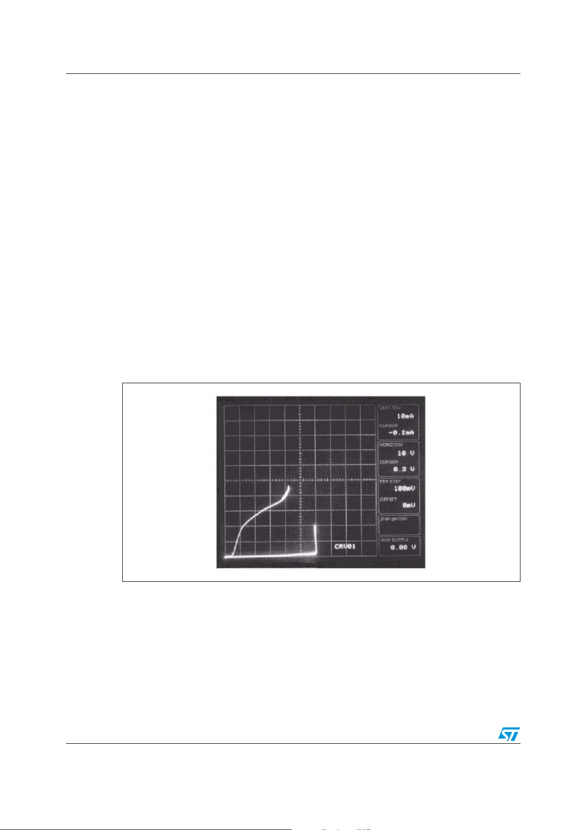
The saturated-drain-source breakdown voltage (BV
) of a MOSFET device is specified at
DSS
a particular value of current with the drain biased and the gate, as well as the source,
shorted. BV
tracer displays for LDMOS breakdown. A BV
can take many forms as represented in Figure 1 which shows the curve
DSS
curve can have a soft breakdown with
DSS
multiple breaks in the curve which is indicative of non-uniformities in the stress within the
inter-digitated cell structure.
Figure 1 shows a BV
curve with characteristics that are typical of a device exhibiting
DSS
punch-through due to an improper body-doping profile. There are four significant areas on
this curve - the low, mid, high and breakdown drain-voltage regions which reflect leakage,
punch-through, space-charge-limited current and avalanche current respectively. Figure 1
also shows a curve with a very sharp break where the current suddenly increases. There
are two significant regions on this curve - pre-breakdown and post-breakdown. Prior to
breakdown, leakage current exists that could be from many sources, such as the normal ptype, n-type (pn) junction leakage due to recombination and generation of carriers in the
quasi-neutral region of the junction. The breakdown-voltage regime is the avalanching of
carriers due to the electric field being greater than the critical electric field (approximately
5
1x10
V/cm). Under these conditions an electron can be accelerated by the electric field.
Due to elastic and inelastic scattering this electron acceleration can generate more than one
carrier and thus a multiplication scheme transpires.
Figure 1. Typical breakdown curves of a LDMOS transistor
Operating near BV
is a reliability risk since the device sustains high-stress conditions.
DSS
Under these conditions the high-energy carriers can alter the device characteristics by
creating, filling and emptying interface traps. For an LDMOS device, if this avalanche
condition exists under or near the gate, the hot carriers can penetrate the gate oxide as well
as alter the on- and off-state characteristics. Typical problems due to this avalanching
include threshold-voltage drift and increased gate leakage. While evaluating devices for this
parameter, large variations are indicative of inconsistencies in device fabrication. For RF
circuit design a general rule of thumb states that the BV
operating voltage in order to support variations in RF voltage.
2/6
should be 2 to 2.5 times the
DSS
Page 3

AN1228 Breakdown voltage
The saturated gate-source current (IGSS) is the leakage current generated when the gate is
biased at a specified voltage while maintaining all other terminals at ground. IGSS leakage
is due to many factors that are related to the integrity of gate oxide and surrounding regions.
Ideally this value would be zero for voltage levels that are less than the voltage required to
reach the dielectric strength of the gate oxide. However, in practice this condition is not
achieved due to the omnipresence of impurities that exist in all wafer fabs and the vagaries
of the oxide growth with the temperature profiles used. IGSS can be used to evaluate the
reliability of this integral component of the MOSFET. An increase of this parameter with a
particular device stress can be used to extrapolate the mean time failure (MTTF) of the gate
oxide. Overstressing the gate either periodically with RF or statically with DC can also cause
an increase in this parameter and thus degrades device performance with respect to RF
power gain. Other considerations for the gate oxide include careful electrostatic-discharge
(ESD) precautions since the gate oxide is easily damaged.
I
is the current produced when the drain is biased at a specific voltage while maintaining
DSS
source and gate contacts at ground. I
has many component contributions. Normal pn
DSS
junction leakage is not a reliability problem as long as it is maintained at a specified value
and does not continue to increase indefinitely. Other sources of I
include minority carrier
DSS
injection from the source due to carriers overcoming the energy barrier resulting from
surface band bending and also from subcritical avalanching caused by high electric fields
due to a non-ideal body as well as the Laterally-Diffused-Drain (LDD) doping profile.
The reverse transfer capacitance C
is the feedback capacitance from the device drain to
gd
the gate that limits MOS device high-frequency gain. This capacitance is a function of many
factors including the gate area, the gate-drain metallurgical overlap as well as the dynamics
of the drain-source depletion spread as a function of drain bias. The three regions of the
capacitance-voltage (CV) characteristics in Figure 2 are indicative of device formation.
Figure 2. Reverse transfer capacitance vs. supply voltage
For LDMOS devices the zero-volt capacitance is mainly due to the gate-oxide capacitance
(C
). The initial decrease in Cgd as bias is applied due to the formation of a depletion
ox
capacitance, dictated by the doping profile that is in series with C
. It is important that the
ox
slope of this initial decrease is large and approaches its final value at some voltage near the
saturated drain-source voltage (V
capacitance (C
) is the capacitance formed between the gate and the ground plane. The
gs
) due to linearity considerations. The gate-source
DS(sat)
LDMOS source, body, epitaxial layer and substrate form the referenced ground plane. The
charge formed by application of a voltage to the gate is dependent on the area of the gate,
3/6
Page 4

Defining ruggedness AN1228
the doping of the body and the metallurgical gate-source overlap. This capacitance is critical
since it is the largest component of the input capacitance and constrains device switching
speed which is comparable to limiting the maximum frequency of operation. C
is the
ds
capacitance formed between the drain and ground plane where the referenced ground
plane is formed by the LDMOS source, body, epitaxial layer and substrate. The charge
formed by application of a voltage to the drain is dependent on the area of the LDD and the
heavily doped drain, the concentration of the epitaxial layer and, to a lesser extent, the body
doping. This capacitance is critical since it is the largest component of the output
capacitance and influences device efficiency.
Device datasheets identify these primary capacitances in the form of C
Capacitance C
combination of C
Capacitance C
(g
) identifies the differential drain current for a differential gate voltage.
fs
is simply the gate-drain capacitance, Cgd, whereas C
rss
and Cgd.
gs
is the parallel combination of Cds and Cgd. The forward transconductance
oss
There are three major regions of the function g
mid-range values g
V
voltages are applied, gfs compresses. For Class AB operation the peak device current
gs
should remain below the g
is usually measured in the g
expands until a linear gfs region is reached. Beyond this region, as high
fs
compression region for maximum linearity. The gfs specification
fs
linear region as shown on device datasheets.
fs
2 Defining ruggedness
The ruggedness or the load-mismatch tolerance of LDMOS technology can be defined in
two ways. The first is that after being subjected to extreme load conditions there is not any
degradation in device performance or output power. A more stringent criterion would be that
there is not any degradation in the device parameters such as a shift in threshold voltage, an
increase in leakage current or a subtle increase in R
can be an indication of long-term reliability problems.
The overall ruggedness of a device when tested in extreme load conditions is related to the
amount of localized thermal stress, the ability to sustain high levels of drain-source current
in BV
near the gate structure.
maximum current capability and the intensity of avalanching occurring under or
DSS
, C
rss
iss
versus Vgs. As Vgs increases from low to
fs
. Changes in these parameters
ds(on)
, and C
iss
oss
is the parallel
.
4/6
Page 5

AN1228 Conclusion
3 Conclusion
The sagacious engineer will take heed of the previously defined parameters and their
relationship to circuit performance and reliability. These parameters can be very helpful
when identifying problems early in the design stage. Other parameters, such as substrate
current, may be even more sensitive but are not always accessible to the design engineer.
The implications of the instability of these parameters are manifold and can ultimately be
expressed from the sub-atomic device physics regime to the circuit performance. This paper
has focused on aspects that the design engineer would consider tractable. By better
understanding the relationship of these basic MOSFET parameters to circuit performance,
designers can more accurately create effective amplifiers and other active circuits.
4 Revision history
Table 1. Revision history
Date Revision Changes
21-Jun-2004 2 Minor text changed
31-Jul-2007 3 The document has been reformatted
5/6
Page 6

AN1228
Please Read Carefully:
Information in this document is provided solely in connection with ST products. STMicroelectronics NV and its subsidiaries (“ST”) reserve the
right to make changes, corrections, modifications or improvements, to this document, and the products and services described herein at any
time, without notice.
All ST products are sold pursuant to ST’s terms and conditions of sale.
Purchasers are solely responsible for the choice, selection and use of the ST products and services described herein, and ST assumes no
liability whatsoever relating to the choice, selection or use of the ST products and services described herein.
No license, express or implied, by estoppel or otherwise, to any intellectual property rights is granted under this document. If any part of this
document refers to any third party products or services it shall not be deemed a license grant by ST for the use of such third party products
or services, or any intellectual property contained therein or considered as a warranty covering the use in any manner whatsoever of such
third party products or services or any intellectual property contained therein.
UNLESS OTHERWISE SET FORTH IN ST’S TERMS AND CONDITIONS OF SALE ST DISCLAIMS ANY EXPRESS OR IMPLIED
WARRANTY WITH RESPECT TO THE USE AND/OR SALE OF ST PRODUCTS INCLUDING WITHOUT LIMITATION IMPLIED
WARRANTIES OF MERCHANTABILITY, FITNESS FOR A PARTICULAR PURPOSE (AND THEIR EQUIVALENTS UNDER THE LAWS
OF ANY JURISDICTION), OR INFRINGEMENT OF ANY PATENT, COPYRIGHT OR OTHER INTELLECTUAL PROPERTY RIGHT.
UNLESS EXPRESSLY APPROVED IN WRITING BY AN AUTHORIZED ST REPRESENTATIVE, ST PRODUCTS ARE NOT
RECOMMENDED, AUTHORIZED OR WARRANTED FOR USE IN MILITARY, AIR CRAFT, SPACE, LIFE SAVING, OR LIFE SUSTAINING
APPLICATIONS, NOR IN PRODUCTS OR SYSTEMS WHERE FAILURE OR MALFUNCTION MAY RESULT IN PERSONAL INJURY,
DEATH, OR SEVERE PROPERTY OR ENVIRONMENTAL DAMAGE. ST PRODUCTS WHICH ARE NOT SPECIFIED AS "AUTOMOTIVE
GRADE" MAY ONLY BE USED IN AUTOMOTIVE APPLICATIONS AT USER’S OWN RISK.
Resale of ST products with provisions different from the statements and/or technical features set forth in this document shall immediately void
any warranty granted by ST for the ST product or service described herein and shall not create or extend in any manner whatsoever, any
liability of ST.
ST and the ST logo are trademarks or registered trademarks of ST in various countries.
Information in this document supersedes and replaces all information previously supplied.
The ST logo is a registered trademark of STMicroelectronics. All other names are the property of their respective owners.
© 2007 STMicroelectronics - All rights reserved
STMicroelectronics group of companies
Australia - Belgium - Brazil - Canada - China - Czech Republic - Finland - France - Germany - Hong Kong - India - Israel - Italy - Japan -
Malaysia - Malta - Morocco - Singapore - Spain - Sweden - Switzerland - United Kingdom - United States of America
www.st.com
6/6
 Loading...