

Page 1
AN1215
APPLICATION NOTE
HOW TO HANDLE SHORT CIRCUIT CONDITIONS
WITH ST’s ADVANCED PWM CONTROLLERS
by Claudio Adragna & Giuseppe Gattavari
Purpose of this note is to provide some advice on how to manage a short circuit condition for a switching
converter controlled by ST's advanced PWM controllers L5991 and L5993.
After a quick review of merits and limits of the current limitation functionali ty embedded in these IC's, a
simple circuit will be given that allows to fulfill designer's typical requirements on what the converter is
supposed to do in case of overload or short circuit.
Current limitation schemes: merits and limits
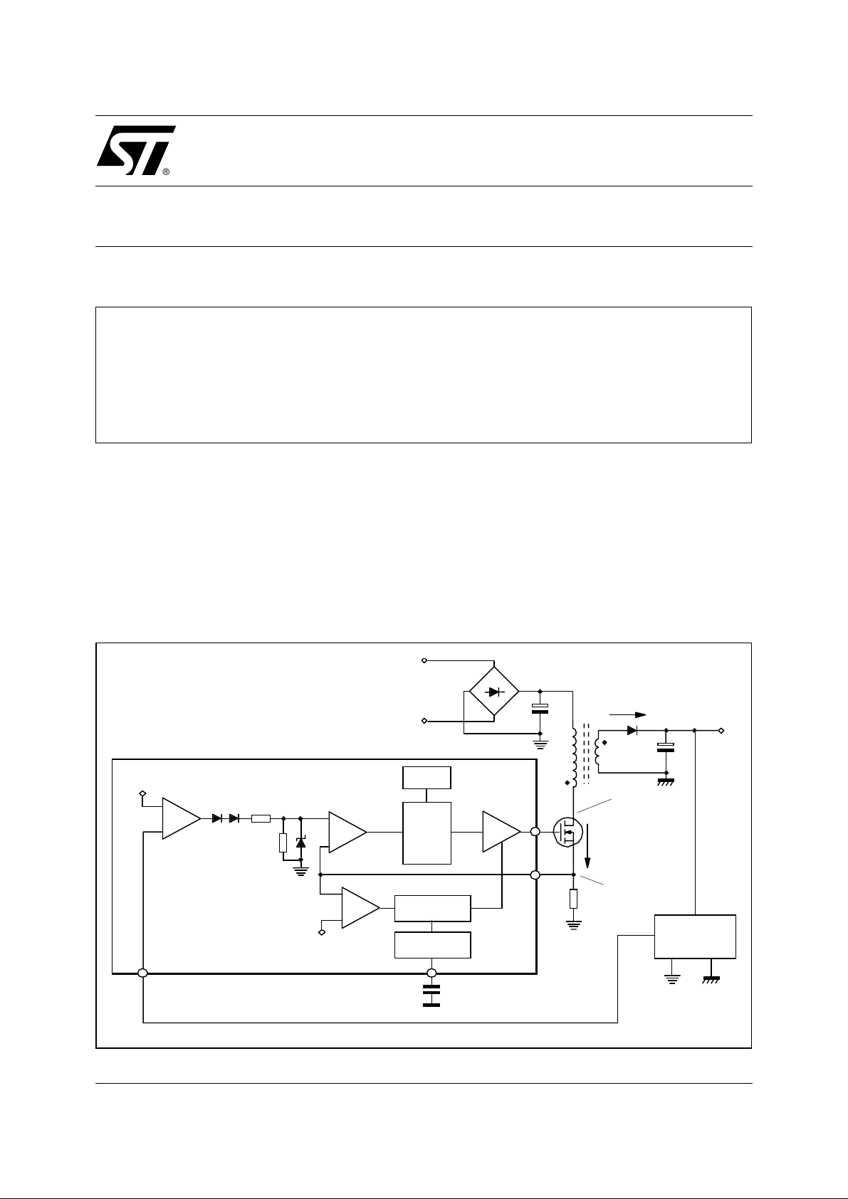
ST's advanced PWM controllers L5991 and L5993 [1] [2] include a two-level overcurrent protection: the "pulseby-pulse" (or "cycle-by-cycle") current limitation and the so-called "hiccup mode" operation.
Pulse-by-pulse current limi tation ideally limits the peak primary current at 1/R
(see figure 1) when the converter
s
is overloaded or there is a l oad sho rt circuit. Even neglecting non- idealities, which worsen the scenari o and must
be accounted for in a safe design, pulse-by-pulse curr ent limi tation just prevents the system from losing control
of the peak primary current. Nothing more.
Figure 1. PWM control and current limiting in L5991 and L5993.
Vin
Is
Lp
Vdrain
Ip
Vcs
Rs
Vout
ISOLATED
FEEDBACK
2.5 V
ERROR
AMPLIFIER
+
-
ADVANCED PWM
CONTROLLER
(L5991, L5993)
2R
R
PWM
COMPARATOR
-
1V
+
+
-
1.2V
Vac
CLOCK
S
R
Q
LATCH
HICCUP
SOFT-START
DRIVER
December 1999
Css
1/7
Page 2
AN1215 APPLICATION NOTE
g
g
g
g
The output current is not limited and may cause PCB traces burning. Converter's power throughput declines
only slightly. Furthermore, power losses get concentrated on some specific parts, e.g. the output rectifier(s),
which may overheat and go towards destruction if not rated for this extreme condition and if heatsinking capability is not generously provided.
When pulse-by-pulse current limitation cannot maintain the peak primary current under control, hiccup mode
protection takes over and halts the resulting current runaway. This happens when the switch ON-time needed
to control the peak primary current is lower than the minimum value T
a result of its internal delays. In L5991 and L5993 T
can be estimated as high as 200 ns, typical value.
ONmin
More details on this "runaway condition" can be found in the appendix.
With reference again to figure 1, in case of current runaway the voltage on the current sense pin will go over 1V.
As it reaches 1.2V a comparator triggers this special functionality [1], [2].
Unlike pulse-by-puls e limitati on, hicc up mode operation keeps outp ut current and power thr oughput very low. It
would be desirable, then, to rely on hiccup operation to conveniently handle a load short circuit. However, it is
quite common that even a dead short at the converter's output cannot activate hiccup protection.
Referring to the appendix for a detailed analysis, high input voltage, high regulated output voltage and high
switching frequency favour current r unaway and, therefore, hiccup operation to be tripped further to a load short
circuit. In many applications, such as AC-DC adapters or PC's silver boxes, where the output voltage is not so
high and the switching frequency is quite low (below 100 kHz) it is extremely likely that the runaway condition
will never be met and the hiccup protection will never be activated. Furthermore, in these applications the load
is usually connected through long cables, then the total short circuit resistance is not low and the T
to control peak current needs not be so short.
that the controller can generate as
ONmin
needed
ON
In other applications, such as monitor SMPS, the runaway condition is likely to be met for the highest output
voltages, especially at high input voltage and if they are synchronized at high frequency.
Actually, hiccup protection serves two different purposes. The first one is related to the capacity of the L5991
and L5993 to be operated at a very high frequency (up to and beyond 500 kHz): to guarantee a safe handling
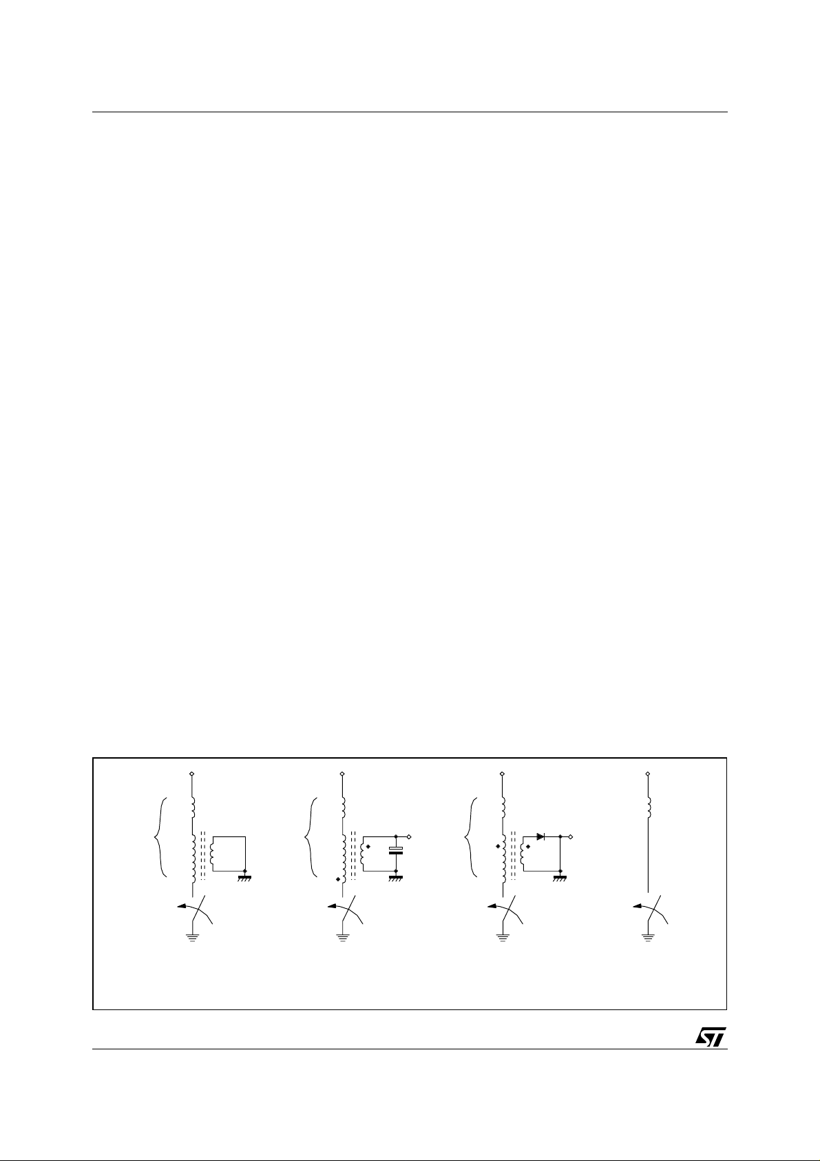
of a load short circuit under all conditions of operating frequency, hiccup protection must be added to pulse-bypulse limitation. The second purpos e is to cover some fault conditions that pulse-by-puls e limitation cannot handle. These are basically:
1. short circuit of the secondary winding (regardless of the topology);
2. secondary catch diode short circuit (in flyback converters);
3. secondary freewheeling diode short circuit (in forward converters).
Figure 2. Fault conditions that activate hiccup mode operation.
Vin
LK
L
P
L
M
L
Vin
LK
L
P
L
M
L
Vin
LK
L
P
L
M
L
Vin
L
LK
Secondary windin
short circuit
(any topolo
y)
Secondary diode
short circuit
(flyback topolo
Freewheeling diode
short circuit
y)
(forward topolo
y)
Equivalent circuit
2/7
Page 3
AN1215 APPLICATION NOTE
µ
µ
All of these conditions reflect a short cir cuit to the transformer's primar y side while the swit ch is ON. The primary
current rate of rise is then limited only by the leaka ge inductance of the transfor mer, which is few percent of the
primary magnetizing inductance (see fig. 4). This means that the current slope will be 30-50 times higher than
in normal operation, thus pulse-by-pulse limitation has no chance to control the current.
Overcoming pulse-by-pulse issues
With the aim of reducing power consumption during an overload or a load short circuit, it is possible to select
one of the following two basic strategies:
1. Making the converter enter hiccup mode operation as a fault is detected and letting it go back into normal operation automatically as the fault is removed (autorestart).
2. Shutting down the converter as a fault is detected and keeping it off until it is disconnected from the
mains. Only after a power-off / power-on cycle the converter is enabled to restart.
Both of these strategies can be easily implemented with ST's advanced family of PWM controllers, thanks to
the numerous functions available. Figure 3 shows how this can be done with the same basic circuit comprising
only four cheap external parts.
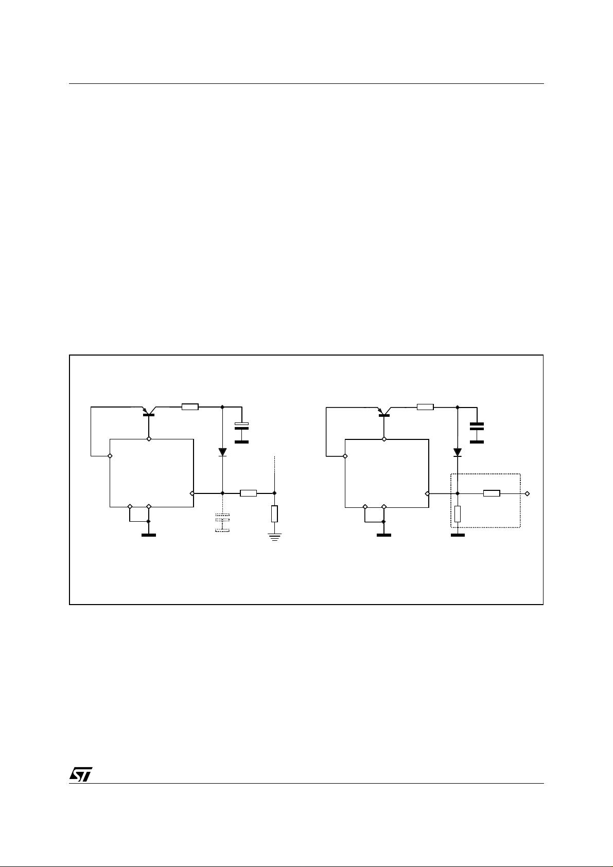
Figure 3. Different strategi es for l ow di ss i pation durin g loa d short circuit
Ω
COMP
6
VFB SGND
BC327
Vref
L5991
L5993
5
3.6 k
4
12
13
Autoresta rt
ISEN
1N4148
1.5 k
10
Ω
BC327
F
COMP
6
Vref
4
L5991
L5993
12
5
Rs
VFB SGND
Shutdown
27 k
14
Ω
DIS
1N4148
R6 330 k
R5
Ω
47 k
0.47
F
Ω
OVP
When in current limitation because of an overload or a load s hort circuit, the output v oltage drops below its regulated value and the output of the error amplifier (pin 6, C OMP) saturates hi gh (≥ 6V) in the attempt of recovering
voltage regulation. This is used for turning on the small-signal PNP (its base is tied at 5V) and getting a current
available for triggering a protection funct ionality . However, a delay of several ms is needed to prevent the function from being activated at start-up or as a result of a load surge. This is simply done with an RC cell. Finally a
diode is needed to decouple the circuit from the others connected to the same pin, during normal operation.
Hiccup is activated by pulling the current sense pin (ISEN, 13) above 1.2V. Error amplifier source capability with
high saturation voltage is about 1 mA, thus the resistor between the current sense resistor and ISEN pin is increased from 1 to 1.5 kΩ. The 3.6 kΩ collector resistor and the 10µF capac itor form a delay cell of about 15 ms.
3/7
Page 4

AN1215 APPLICATION NOTE
Fi
This circuit has been impl emented in a 45W, wide ra nge
mains AC-DC Adapter with the L5991 [3] and the results
are shown in fig. 4.
Shutdown will be activated by injecting the curr ent deli vered by the PNP into pin 14 (DIS) so that the voltage at
gure 4. Input power vs. input voltage during
hiccup mode operation
Pin [W]
7
6
the pin exceeds 2.5V. The resistor divider R5-R6 refers
to the circuit described in [3] and is part of the latched
OVP circuit. In case of a different value of R5, the collector resistor and the delay capacitor will be changed consequently.
Besides increasing safety, the advantage of each of
these techniques is that heatsinking of the power parts
needs to be designed neglecting anomalous operating
conditions (overload or short cir cuit), with a considerabl e
saving of size and cost.
5
4
3
2
1
50 100 150 200 250 300 350 400
L5991-based 45W AC-DC Adapter
Dead short at output
Vin [V]
Conclusions
Pulse-by-pulse and hiccup mode current limitation are the ways ST's advanced PWM controllers L5991 and
L5993 handle overload and shor t ci rcuit c onditions . It has been sho wn that these tw o func tions c over two differ ent fault categories: pulse-by-pulse does not allow the power throughput to rise out of control in case of a load
failure whereas hiccup usually protects against short circuits inside the converter itself (transformer, diodes)
where pulse-by-pulse is not effective.
Unlike hiccup, which dramatically reduces power throughput, pulse-by-pulse limitation little does about that,
thus forcing designers to oversize heatsinking of the critical parts for the sake of safety.
A simple and ver satil e c ircuit has been presented that helps over c ome thi s probl em and can be used to achi eve
two common protection schemes, autorestart and shutdown, resulting in very low power dissipation.
As an appendix, a calcu lation method that helps evaluate whether a l oad shor t ci rcuit ca n activate hiccup mode
protection or not in a given application, is provided.
REFERENCES
[1] "L5991/A Primary Controller with Standby" Datasheet
[2] "L5993 Constant Power Controller" Datasheet
[3] "45W AC-DC Adapter with Standby Function" (AN1134)
4/7
Page 5

AN1215 APPLICATION NOTE
APPENDIX
Will hiccup mode be activated or not ?
Basically, hiccup mode will be activated if the control is not able to guarantee a steady-state operation for the
converter under a given short circuit condition.
Like in normal operation, under overload or short c ircuit conditio ns a steady- state operation requires volt·second
balance across the storage element of magnetic energy: the transformer in a flyback converter and the output
inductor in a forward. Otherwise, c urrent runaway will occ ur: energy rise insi de the magnetics dur ing MOSFET's
ON-time exceeds ener gy decay during OFF-time, thus current will raise with no c ontrol saturating the magnetics
and leading to converter destruction.
The condition for the current runaway to occur (runaway condition) will be derived for both flyback and forward
topology. Please refer to the end of the appendix for symbol explanation.
Flyback topology.
The balance condition (assuming the system is working in continuous current conduction,
which is extremely likely under overload condition and absolutely certain in short circuit) is:
–()⋅=
(A1).
Solving eqn. (A1) for T
⋅
VinT
ON
yields the switch ON-time. This is applicable during both normal operat ion and pulse-
ON
V
RTswTON
by-pulse current limitation:
V
R
ON
--------------------- -
VinV
T
It is worthwhile reminding that the reflected voltage V
nVoV
V
R
Whereas in normal operation V
V
drops and so does VR. Their value will be dependent on t he total resis tance of the sec ondary circuit, including
o
is regulated and, therefore, VR is constant, in case of overload or short circuit
o
⋅=
T
+
R
R
is given by:
+()⋅=
F
(A2).
sw
(A3).
diode, secondary winding wire, PCB tracks, and the short circuit resistance. Obviously, the more severe the
overload, the lower the total resistance, and the lower V
Eqn. A2 shows that, as the overload gets closer to a short circuit, T
sulting from (A2) is l ower than T
, the shortest switch ON-time that the control ler can gener ate (200 ns typ.
ONmin
.
o
ON
gets shorter and shorter. If the time re-
in the L5991 and L5993), then the contr oll er wi ll not be a ble to maintain the vo lt·second balance and the current
will begin to rise with no control.
Combining equations (A2) and (A3), the runaway condition, that is the condition for hiccup operation to be invoked, is:
nV
----------------------------------------------- -
V
in
+()⋅
oVF
nVoV
+()⋅+
F
≤⋅
T
swTONmin
(A4)
It is possible to estimate the left side of eqn. A4 assuming V
will be greater than zero thus T
will be in this way underestimated.
ON
= 0 (ideal short circuit). In real-world condition Vo
o
Ideally, eqn. (A4) becomes:
⋅
nV
in
F
⋅+
nV
T
swTONmin
F
≤⋅
(A5)
5/7
-----------------------------
V
Page 6

AN1215 APPLICATION NOTE
In this equation it is reasonable to assume VF = 1V for a Schottky diode and VF = 1.5 V for a p-n type.
The inspection of (A5) shows that the conditions that favour current runaway are a high input voltage Vin, a high
switching frequency (i. e. a shorter T
breakdown issues (typically around 100V), the higher V
Forward topology.
The balance condition (continuous c urren t conducti on is i n use ev en in normal oper ation) for
the output inductor is:
V
in
------- -
n
ON
Solving eqn. (A6) for T
yields the switch ON-time:
Considering equation (A7), the runaway condition for a forward converter is:
Ideally, with V
= 0, this equation becomes:
o
where it can be assumed again V
Like in flyback topology, the conditions that favour current runaway are a high input voltage, a high switching
frequency and a high regul ated output v oltage. H owever, comparing equations A5 and A9 under the sam e conditions of n, V
, Vin and Tsw, it is possible to note that forward converter is less prone than flyback to current
F
runaway. This is reinforced b y the fact, not v isibl e in the abov e equations, that in a forward co nver ter the output
inductor resistance will always be part of the short-circuit current loop.
) and a high regulated output voltage: in fact, being VR fixed by MOSFET
sw
, the lower n.
o
–
–
V
F
= 1V for a Schottky diode and VF = 1.5 V for a p-n type.
F
⋅
V
T
o
ON
=
T
n
n
ON
+
V
V
o
------------------- -
V
in
⋅
nV
F
-------------- -
V
in
⋅⋅
F
T
+()
V
oVF
+
V
oVF
------------------- -
V
T
swTONmin
T
in
≤⋅⋅
swTONmin
≤⋅
T
(A7).
sw
(A9)
–()⋅=
swTON
(A8)
(A6)
Symbol list
Symbol Description
V
in
V
o
T
ON
T
ONmin
V
R
T
sw
n Transformer's primary-to-secondary turn ratio.
V
F
6/7
Converter's DC input voltage.
Converter's output voltage.
Power switch ON-time.
Minimum switch ON-time manageable by the PWM controller IC.
In flyback, secondary voltage reflected back to the primary during secondary rectifier conduction.
Switching period, equal to the reciprocal of the converter's switching frequency.
Forward drop across secondary rectifiers (catch and freewheeling diode)
Page 7

AN1215 APPLICATION NOTE
Information furnished is believed to be accurate and reliable. However, STMicroelectronics assumes no responsibility for the consequences
of use of such information nor for any infringement of patents or other rights of third parties which may result from its use. No license is granted
by implic ation or otherwise under any patent or patent r i ght s of STMi croelectr oni cs. Specifications menti oned in thi s publication are s ubj ect
to change without notice. This publication supersedes and replaces all information previously supplied. STMicroelectronics products are not
authorized for use as cri tical components in li f e support dev i ces or systems without express writ t en approval of STMicroel ectronics.
The ST logo is a registered trademark of STMicroelectronics
1999 STMi croelectronics - All Ri ghts Rese rved
Australi a - Brazil - China - Finland - Fr ance - Germany - Hong Kong - India - Italy - Japan - Malaysia - Mal ta - Morocco - Singapore - Spain
STMicroelectronics GROUP OF COMPANIES
- Sweden - Sw itzerland - United Kingdom - U. S .A .
http://www.s t. com
7/7
 Loading...