

AN1214
APPLICATION NOTE
DESIGN TIPS FOR L6561 POWER FACTOR CORRECTOR
IN WIDE RANGE
by Cliff Ortmeyer & Claudio Adragna
This application note will describe some basic steps to optimize the design of the L6561 PFC for wide
range voltage input (105V- 300V) while also having a broad output power range (65W - 105W). Initial
design steps are covered in application note AN966. This is to serve as a supplement to that application note and also give an example of a wide range demo board optimized for the US market (110V 277V). A deeper look at the control of the L6561 can also be found i n applica tion note AN1089 “Control
loop modeling of L6561-based TM PFC”.
Introduction
Designing a PFC circuit with a singula r input voltage and a singul ar output power is a task that is rather straight
forward and gives a very good set of component values when the design equations are used. The task becomes
a little more difficult when a wide range PFC is needed and the specifications are tight. This is common in applications such as lighting w here ther e is a deman d for good power factor ( >.99) and THD less than 10% in the
full range of nominal operating conditions. The problem occurs since the design must be done for the worst
case conditions which are a low input voltage and maximum output power. As we w ill s ee, this will diminis h the
performance of the PFC circuit when the input voltage is high and the output power is low. What must be done
in this case i s to lo ok clo sely a t the lim its of the L6561 and exter nal co mponents and to optimiz e or compr omi se
where needed.
Design Tips
Multiplier Operation
. Once the initi al design is done and measurements have been made, the next step is to look
at the operating parameters of the L6561 to see that it is worki ng within its ful l capabi lities with out going ove r its
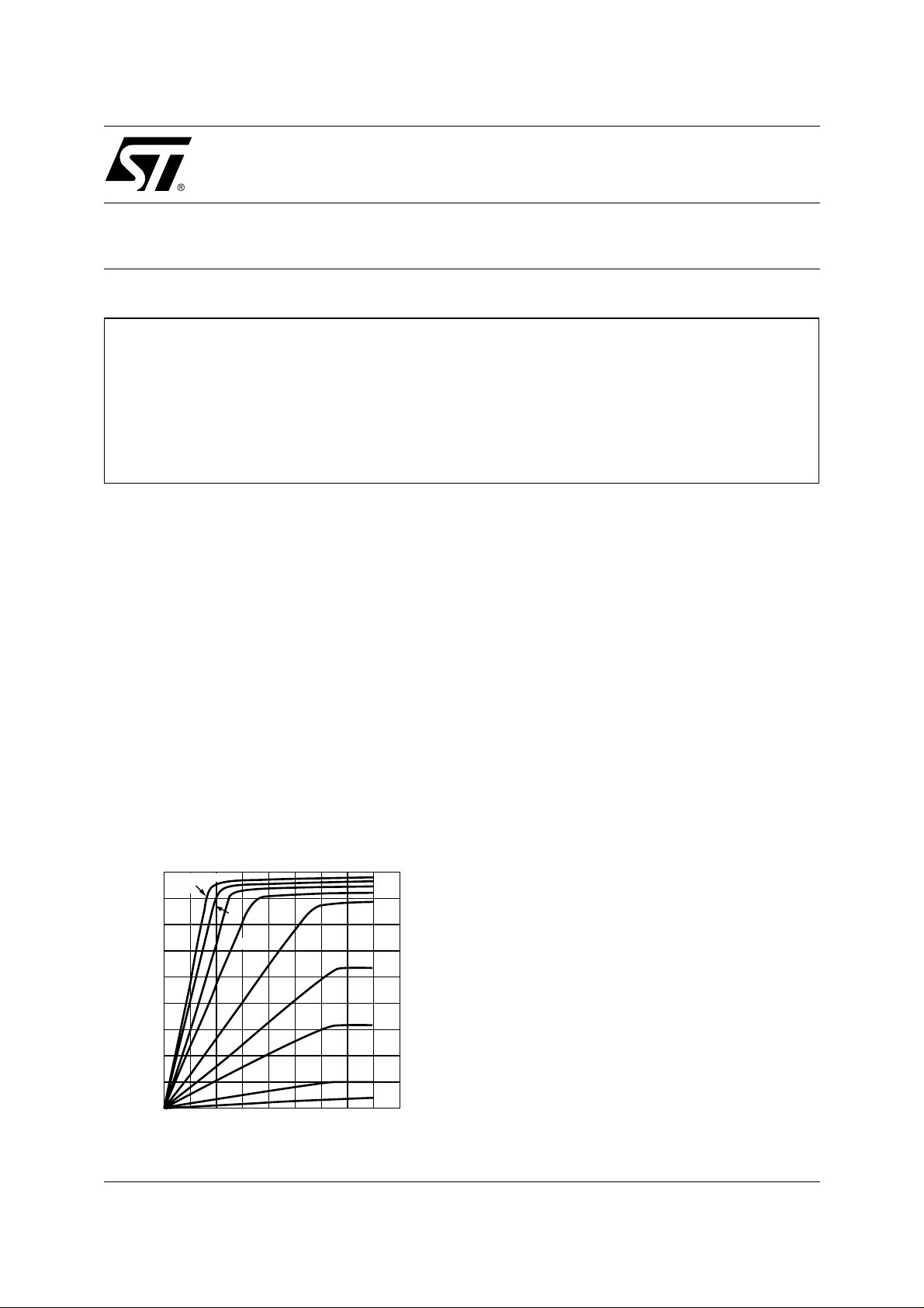
linear operating range. A copy of the table we will be referring to is shown in Fig. 1.
Figure 1. Multiplier Characteristics
(pin4)
V
CS
upper voltage
(V)
clamp
1.6
1.4
1.2
1.0
0.8
0.6
0.4
0.2
0
0 0.5 1.0 1.5 2.0 2.5 3.0 3.5 4.0 4.5
December 2000
5.0
4.5
4.0
V
MULT
D97IN555A
(pin3) (V)
V
COMP
3.5
3.2
3.0
2.8
2.6
(pin2)
(V)
For optimal operation the device should stay in the
linear operation of the multiplier. As can be seen,
there are three pins that should be measured in the
worst case conditions. The first is with the lowest input voltage (low line) and the highest output power.
The second is at t he hig hest i nput v oltage ( high line)
and the lowest output power. The first pin to be
measured is the Vcomp (pin2). This is the output of
the error amplifier (Figure 2) and will determine
which curve will be referenced when measuring the
other two parameters - Vcs and Vmult. Once this is
established, the peak voltage of the multiplier input
(pin 3) should be measured and noted. Next measure the peak voltage of the current sense resistor
(Vcs - pin 4). Looking at the graph in Figure 1, determine which curve to use from the Vcomp v oltage.
1/6
AN1214 APPLICATION NOTE
Next, note where the Vcs and Vmult are on the curve to make sure that they are in the linear operating region.
If operation in the linear region is not met, adjust the variable that allows linear operation to be met. If however
the device is operating in the linear region but is not allowing the full range of the multiplier to be used, then
increasing one of the variables (the mul tiplier voltage for exam ple) can help to maximize the full operating r ange
of the multiplier.
Figure 2. Multiplier Block Diagram.
Rs
23
X
4
-
CURR.CMP
+
E/A
1.7V
D97IN675
Zero crossing dead time
. Once the multiplier operating parameters have been met, the input voltage as well as
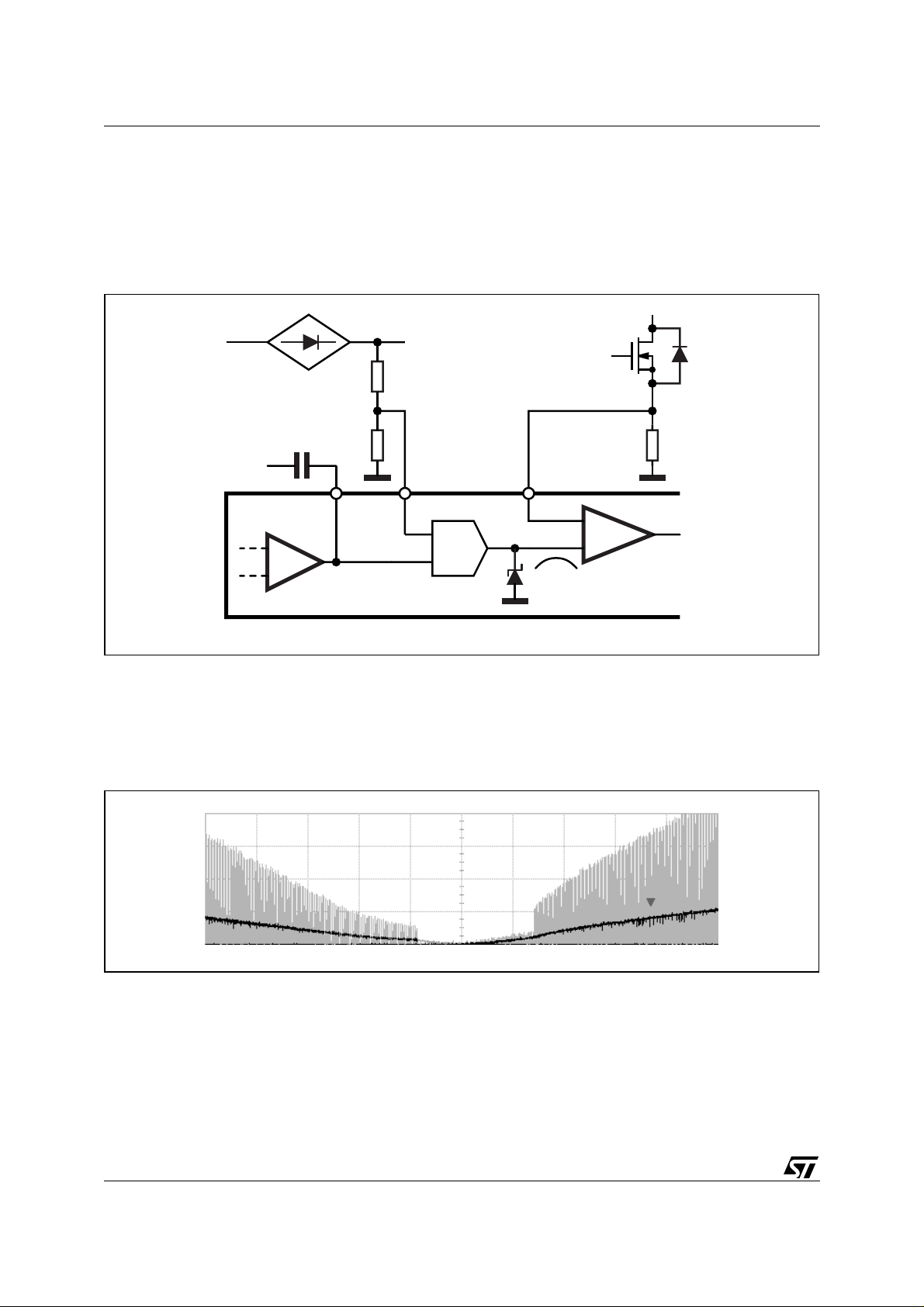
the input current should be looked at together. One problem to look for is a distortion of the current waveform
especially at high line and low load. An example can be seen in figure 3.
Figure 3. Current Shape at Zero Crossing with High Capacitance FET and slow Turn-on Diode.
The main reason for this effect is that near zero-crossings the energy stored in the inductor is very low, not
enough to charge up the drain node total capacitance (basically, the FET’s drain-to-source capacitance C
oss
and the inductor’s parasitic intrawinding capac itance) to turn the boost diode on. The turn-on speed of the boost
diode adds to the problem as well. As a result, energy is exchanged betw een reactiv e components an d there is
no input-to-output transfer. This can be seen in figure 3.
To minimize Coss, the Rds
of the FET sh ould be max imized within the limits of acc eptable conducti on l oss-
(ON)
es, and its voltage rating s hould be the mini mum that sti ll provid es adequate br eakdown capability. In fact, both
2/6

AN1214 APPLICATION NOTE
a low Rds
and a high voltage imply a higher C
(ON)
oss
.
Inductor parasitic capacitance can be reduced by minimizing the number of winding layers. Adding a layer of
tape between winding layers can reduce the capacitance cons iderably. The use of a slotted bobbin is al so very
effective.
Also optimizing the diode can offer a positive contribution. A minimum junction capacitance will be somewhat
beneficial, even though this is a minor contribution to the total drain capacitance.
A major improvement c an be offered by a diode with a well contr olled die resi stivi ty (such as Turbosw itch series)
which has a low er peak forward voltage, so that it actually turns on j ust a few volts above the PFC output voltage.
An example of the improvement given by optimizing the FET and the diode is shown in figure 4.
Figure 4. Current Shape at Zero Crossing with Lower Capacitance FET and Turboswitch Diode
Input capacitance (EMI fi ltering).
Another source of error can be du e to the input fil ter. Si nce the vol tage output
from the rectifier bridge is used as the reference for the current to follow, any distortions in this waveform will
translate into distortions of the current waveform, hence lower power factor or greater THD. One cause of this
can be due to too large of a high frequency filter capacitor being used after the bridge. A high value capacitor
can filter the r ectified voltage and cause the v oltage to devi ate fr om a recti f ied s inusoid and even n ot reach zero
at light load. This can be seen in figure 5.
Figure 5. Non-discontinuous Voltage Error
The obvious way of improving this is to lower the high frequency capacitor value. Care must be taken not to
lower the capacitance such that the effectiveness of the EMI filter (in front of the diode bridge) is not degraded
so as to not pass regulatory requirements. So, by lowering that capacitance, the HF filter capacitor in front of
the diode bridge may need to be increased.
Switching frequency.
One other method of using the full dynamic range of the L6561 is to reduce the minimum
switching frequency of the FET. By using the lowest possible switching frequency of the L6561, a wider range
3/6

AN1214 APPLICATION NOTE
of switching frequencies are available to be used. This helps minimize the effects of the internal propagation
delay as well as the offset of the current sense comparator. In this way the current will track the voltage waveform better, in particular near the zero-crossings. This, however, must be weighed against the size increase of
the inductor because a lower switching frequency implies a larger inductance value.
When determining the lowest fr equency, it must be noted that switching below 15kHz is not r ecommended since
this may interfere with the internal starter.
A special construction technique of the inductor can offer the optimum compromise: one that allows the use of
a low inductance value so as to min imize inductor s ize and, at the s ame time, have a lower switching frequenc y
near zero-crossings. The price to pay for that is an additional step in the inductor manufacturing flow.
It is the so-called “step-gap core” technique: the centre leg of one half of the ferrite core is ground so that the
air gap thickness has a step change, as shown in fig. 6.
At low inductor current the small thinner part of the air gap dictates a high inductance value (L1). As current
increases above a certain value (I
tance will drop to a value (L2<L1) determined by the thicker part of the air gap (l
introduced so that, for a given switching frequency at the top of the rectified sinusoid - where current is high (that is, for a given L=L2), the switching frequency near the zero-crossings - where current is low - will not go
as high as with a linear inductor.
Figure 6. Step-gap ferrite grinding and its effect on inductance value
), the thinner part of the air gap will progressively saturate and the induc-
L1
). A non-linear ity is delibe rately
g
b
"step-gap"
h
g
l
L
L1
core half
L2
L2
IL1I
The appropriate height h and breadth b of the ferrite step (both of them determine L1 and IL1) for a given application will be found empirically.
L
I
4/6

AN1214 APPLICATION NOTE
Wide Range Example Circuit
An example circuit was designed with a varying voltage input of 110V to 277V and an output power of 65W to
105W. The techniques in this paper (except the step-gap core) were used to help bring the power factor and
THD into acceptable levels. The example schematic and associated EMI filter are shown below along with the
measured results.
Figure 7. Example Schematic
FUSE 4A/250V
Vac
(105V to 305V)
NTC
(*) R3 = 2 x 120KΩ
R6 = 1Ω/2
R7 = 2 x 499KΩ, 1%
R9 = 2 x 620KΩ
BRIDGE
4 x 1N4007
+
-
D1 STTA106
68K
5
L6561
6
T
C3 1µF
21
7
4
R7 (*)
R5 MOS
STP6NB50
10
R6 (*)
0.5
1W
D99IN1098
C7
10nF
R2
100
C6
12nF
R1
8
3
R3 (*)
D3 1N4150
240K
C1
R9 (*)
33nF
1.24M
630V
R10
10K
TRANSFORMER
T: core THOMSON-CSF B1ET2910A (ETD 29 x 16 x 10mm) OR EQUIVALENT (OREGA 473201A8)
primary 90T of Litz wire 10 x 0.2mm
secondary 7T of #27 AWG (0.15mm)
gap 1.25mm for a total primary inductance of 0.8mH
D2
1N5248B
C2
22µF
25V
998K
R8
5.6K
1%
R11
1M
R12
1M
+
Vo=450V
Po=105W
C5
47µF
250V
C5'
47µF
250V
-
Figure 8. Emi Filter
T1 T2
LINE PFC
EARTH
Table 1. Example Schematic Results
Vin
)
[V
AC
105 449 136 0.998 4.7 66.4 61.0 91.9
120 449 136 0.998 5.3 65.8 61.0 92.7
277 449 136 0.995 9.7 65.0 61.0 93.9
300 449 136 0.993 11.0 65.0 61.0 93.9
105 449 237 0.999 4.0 115.8 106.5 92.0
120 449 237 0.999 4.0 114.7 106.5 92.9
Vout
[V]
Iout
[mA]
C
x
C
y
D97IN680
PF
THD
[%]
Pin
[W]
Pout
[W]
Efficiency
[%]
277 449 237 0.997 7.7 111.0 106.5 96.0
300 449 237 0.994 11.2 111.0 106.5 96.0
5/6

AN1214 APPLICATION NOTE
Information furnished is believed to be accurate and reliable. However, STMicroelectronics assumes no responsibility for the consequences
of use of such information nor for any infringement of patents or other rights of third parties which may result from its use. No license is granted
by implic ation or otherwise under any patent or patent r i ght s of STMi croelectr oni cs. Specifications menti oned in thi s publication are s ubj ect
to change without notice. This publication supersedes and replaces all information previously supplied. STMicroelectronics products are not
authorized for use as cri tical components in li f e support dev i ces or systems without express writ t en approval of STMicroel ectronics.
The ST logo is a registered trademark of STMicroelectronics
2000 STMi croelectronics - All Ri ghts Rese rved
Australi a - Brazil - China - Finland - Fr ance - Germany - Hong Kong - India - Italy - Japan - Malaysia - Mal ta - Morocco - Singapore - Spain
STMicroelectronics GROUP OF COMPANIES
- Sweden - Sw itzerland - United Kingdom - U. S .A .
http://www.s t. com
6/6
 Loading...