Page 1

AN1213
APPLICATION NOTE
TDE1707 NOISE IMMUNITY, SH ORT CIRCUIT AN D REVERSE
OUTPUT PROTECTION CHARACTERISATION
by Matteo Uccelli
The TDE1707 is a power switch ( I.P.S) especially dedicated to proximity detectors. For the characteristics
of the I.P.S. please refer to the data sheet and AN485.
Since the device oper ates in Industrial environment, it i s very important a good noi se immunity. The overload
(up to short circuit) and the output reverse connection hardiness are also key point for a device used in this
applications.
EMC testing.
This Evaluation section describes the noise immunity results. For reference, the test has been done as comparison between the TDE1707-B , improved version and the previous one (Old version).
All of the statements regarding burst immunity refer to measurements done in ESALI (European System Application Lab Industrial).
The application laboratory is provided with an appropriate testing bench realised basing on directives contained
in IEC 801/4 normative.
The correlated instrumentation consists of :
- Key Tek ( Thermo Voltek ), CE MASTER EMC immunity test system : surge and burst generator.
- Tektronix TM502 : current probe
- GOULD Data SYS 944 MHz - 500 Ms/sec : digital storage oscilloscope
- Laboratory Power Supply PS-2403 : power supply
The behaviour of the dev ice was m onitored with a current probe on the load, which seems to have less influence
on the measurements. Anyway it is important to pay attention because even when using a current probe it is
really easy to couple additional noise, and of course the result consists in the achievement of lower immunity
levels than the right ones: the fast transients should be coupled only thanks to the capacitive coupling clamp.
For the same reason caution is mandatory regarding the power supply: this one should not be directly affected
from the burst generator . Additional coupling becomes easier and easier as the burst voltage increases: parasitic antennas becomes more efficient.
Table 1. IEC 801/4, limiting values of burst impulses
severity test voltage on signal line
42kV
31kV
20.5kV
1 0.25kV
Testing configuration:
Old ( TDE 1707) and new ( TDE 1707 Rev. B ) silicon have been tested and compared regarding fast transient
( burst ) immunity. This testing was performed on several layouts taking care to operate in the same test conditions.
December 1999
1/7
Page 2

AN1213 APPLICATION NOTE
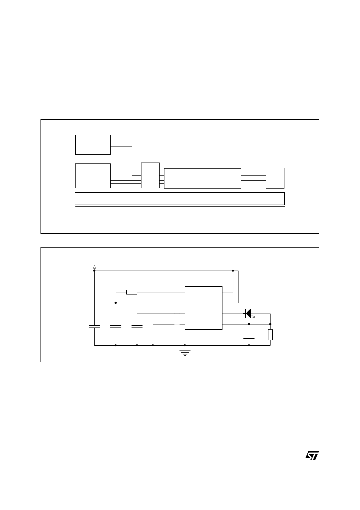
The input pin was connected to Vreg tanks to a 4,7 kOhm resistor (R1), the device was supplying a 220 Ohm
resistor (R2)
The cable to the load was a flat , parallel wires,2 m long cable. Tests were performed with a power supply voltage varying between 18 and 30 V. Capacitors C4, C2 and C3 were smd ceramic capacitors, C1 was a ceramic
no-smd capacitor (smd capacitor for C1 gives no benefits). On Vcc (C4) a 100nF was used , while on Vreg
(C2) a 10nF was adopted, this for all of the tests.
Figure 1. Bench exemplification
Auxiliary
Equipment
Burst
Generator
Ground reference plan
Load
Capacitive coupling clamp
Insulation Support
Signal and
supply
lines
EUT
Figure 2. Application schematic
+V
U1
5
6
3
4
TDE1707
In
Vrg
CAP
GND
Vss
LSO
LD
HSO
7
8
D1
1
2
LED
R2
C3
x
220
C4
100nF
R1
4.7 k
C2
10nF
C1
x
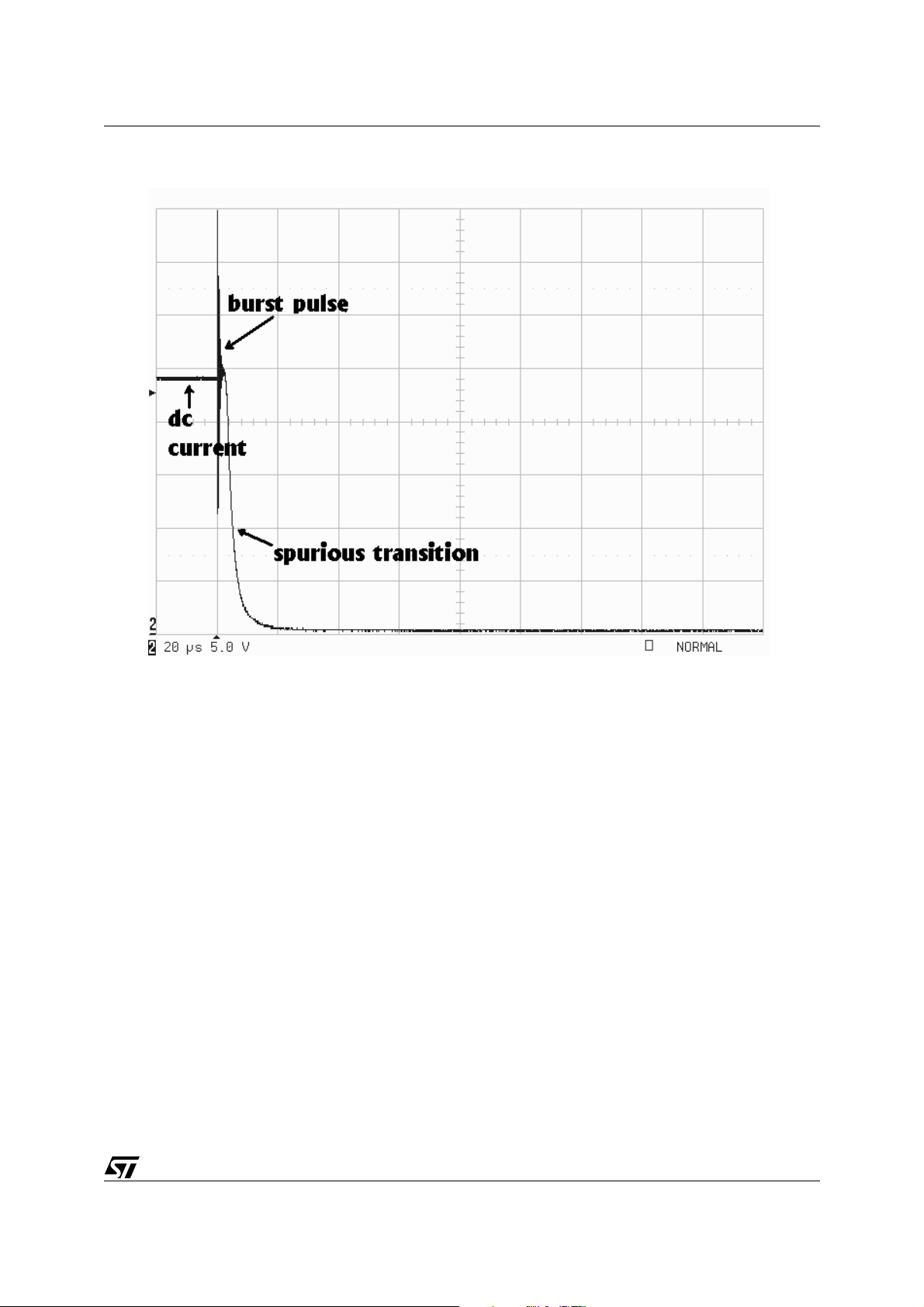
Typically a burst exceeding the tolerance level causes the output transistor to switch off even if the input has
not changed its high state.
2/7
Page 3

AN1213 APPLICATION NOTE
Figure 3. Spurious transition of the output transistor due to burst pulse
TDE 1707 ( old silicon ):
the value of the delay capacitor (C1) does not influence the immunity level of the
device. The device behaves exactly the same whatever it is the value of the capacitor. Without any other capacitor than the two on Vcc ( C4 ) and on Vreg ( C2 ) the device shows an immunity level of +300 / -800. The
immunity can improve if it is adopted a capac itor on the output ( C3 ). This capacitor has the same effec t whenever it is connected between ground and output or Vcc and output. With C3=1 nF the immunity level is +1400
/ -2500 V, C3=10 nF bring to an immunity level higher than +2500 /-2500.
TDE 1707 Rev. B ( new silicon ):
placing the delay capacitor (C1) result s in loweri ng the fast transi ent immunity , which is anyway higher than the one acquired in the same conditions with the old silicon. In fact without
capacitor on pin 3 the device is working correctly even with +2500 / -2500 V of burst voltage. This value is
strongly reduced w hen a delay capac itor is adopted: with C1 = 470 pF, i mmunity drops to +600 / -1500 V. The
same for higher values of C1 ( ex: 3.3nF ). Even with TDE1707 rev.B it is very useful to filter the output and 1
nF between ground and output (C 3) or between Vcc and output it is sufficient to gain the correct operating of
the device with a burst amplitude of +2500 / -2500.
Layout:
anyway it must be underlined the importance of the layout . To gain the highest levels of immunity it is
important to provide an accurate layout for the ground. Star connecti on is recommended for the ground connections of the capacitors on Vcc and Vreg.
3/7
Page 4

AN1213 APPLICATION NOTE
Figure 4. Zoom of th e Lay o ut
Table 2. Immunity levels for old and new silicon corresponding to C out value
Cout (nF) TDE1707 TDE1707 Rev. B
No capacitor -800 / +300V -1500 / +600V
1nF -2500 / +1400V >(-2500 / +2500V)
10nF >(-2500 / +2500V) >(-2500 / +2500V)
Short circuit and reverse output connection behaviour:
The following evaluation refers to the TDE 1707 rev. B operating with a supply voltage varying between 18 and
30 V, pure resistive load (from 0 to 15 k ohm ), ceramic capacitor on Vcc ( 110 nF ) and Vreg (10 nF )
The TDE 1707 cannot withstand short circuit condition without a delay capacitor connected to pin 3.
When the device is switched on from a cold state there is a zone corresponding to which the protection has no
effect on the output transistor: pin 3 goes low but the output transistor does not switch off as it should. This zone
becomes shorter and shorter with rising temperature and finally it is no longer present: when the device is
switched on warm , the protection is fully working. This period of time in which the protection has no effect is
long enough to have destroying effect on the device if the voltage supply is higher than 24 V. It is possible to
see figure 5 this behaviour ( ch. 1 : Vcc, ch. 3: pin 3, ch. 4: I out ).
It is not possible to filter this effect directly on Vcc and Vreg , at least not for reasonable values of electrolytic
capacitors paralleled to the ceramic ones. It is just sufficient to add a very small capacitor (68pF ) on pin 3 to
have no longer this effect and to avoid the problem.
4/7
Page 5

AN1213 APPLICATION NOTE
Figure 5. Short circuit pro t ect io n f ail ur e at tur n on ( no capacitor on pin 3, device cold)
Figure 6. Shor t circu it protection ful ly wo rk i ng (68p F on pin 3, device co ld )
5/7
Page 6

AN1213 APPLICATION NOTE
In case of reversal connection of the output (output of the device tied to supply ground and device ground to
load - tested loads: from 0 to 15 k Ohm) it is required a greater capacitor than in pure short circuit case (220
pF) in order to safely run the device.
Table 3.
Worst case:
Short circuit Reverse output connection
Minimal C delay value:
68pF 220pF
Conclusions:
Table 2 well highlights the impr oveme nt, in terms of noi se immunity, of the actual sili con versio n. Moreover , using the appropriate filters (this means: output capacitor, delay capacitor...), it is possible to safely use the
TDE1707 in its typical env ir onment, and it results to be pr otec ted from poss ible i njuries due to inc idental wrong
connections.
6/7
Page 7

AN1213 APPLICATION NOTE
Information furnished is believed to be accurate and reliable. However, STMicroelectronics assumes no responsibility for the consequences
of use of such information nor for any infringement of patents or other rights of third parties which may result from its use. No license is granted
by implic ation or otherwise under any patent or patent r i ght s of STMi croelectr oni cs. Specifications menti oned in thi s publication are s ubj ect
to change without notice. This publication supersedes and replaces all information previously supplied. STMicroelectronics products are not
authorized for use as cri tical components in li f e support dev i ces or systems without express writ t en approval of STMicroel ectronics.
The ST logo is a registered trademark of STMicroelectronics
1999 STMi croelectronics - All Ri ghts Rese rved
Australi a - Brazil - Ca nada - China - France - Germ any - Italy - Japan - Ko rea - Malays ia - Malta - Mexico - Moro cco - The Netherlands -
Singap ore - Spain - Sw eden - Switzerland - Taiwan - Thail and - United Kingdom - U.S.A.
STMicroelectronics GROUP OF COMPANIES
http://www.s t. com
7/7
 Loading...