

Page 1

AN1132
®
APPLICATION NOTE
90W SMPS FOR MONITORS WITH STANDBY FUNCTION
by Claudio Adragna
Purpose of this note is to provide a brief summary of the specifications and the functionality of the application board implementing a 90W multioutput SMPS for monitors, based on t he L5991, current
mode PWM controller.
Evaluation results are also presented so as to underline the benefits offered by the L5991 in such a
new generation of SMPS that r equires a superior ef ficiency in standby conditions, aim ing at compliance with energy saving standards.
Design Specifications
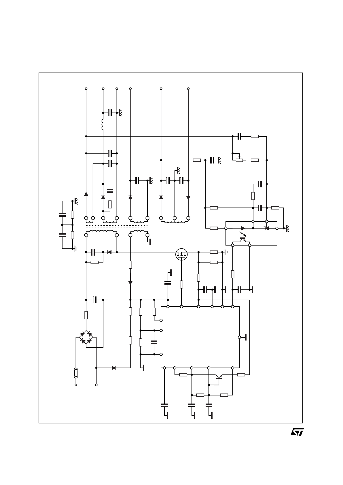
Table 1 summarises the electrical specification of the applic ation. The complete electrical schematic is
shown in fig. 1 and the bill of material is listed in Table 2.
Table 1. Design Specification
Input Voltage Range (Vin) 88 to 264 Vac
Mains Frequency (fL) 50/60 Hz
Maximum Output Power (P
Outputs
Switching Frequency in Normal Mode (f
Switching Frequency in Suspend / OFF mode (fSB) 18kHz
Target Efficiency (@ Pout =90W, Vin =88 ÷264 Vac) (η) > 80%
Maximum Input Power (@ Pout = 0.5 W, Vin =88 ÷ 264 Vac)
) 90W
out
Horizontal Deflection
Video Amplifier
Vertical Deflection
Heater
) 40kHz
osc
V
I
out
Full load ripple = 1%
V
I
out
Full load ripple = 1%
V
I
out
Full load ripple = 1%
V
I
Full load ripple = 2%
= 200V
out
= 0.325A
= 80V
out
= 0.125A
= ±15V
out
= 0.33A
= 6.3V
out
= 0.8A
out
2W
≤
The selected topology is flyback. The operation mode (@ Pout = 90W ) is CCM (Continuous Conduction
Mode) at low mains voltage, DCM (Discontinuous Conduction Mode) at high mains voltage. This design
choice relieves the stress on the power components at low mains voltage, compared with a full DCM solution.
The application will benefit from the features of the L5991 PWM controller in order to minimise the power
drawn from the mains under light load conditions: low start-up and quiescent currents, and Standby
function.
September 2000
1/12
Page 2
AN1132 APPLICATION NOTE
Figure 1. Electrical Schematic.
200V
D07 BYT11-800
18
1
C01 4700pF 4KV C02
R31 4.7M R32 4.7M
65W
H1 1µH
D08 STTA106
17
C10
47nF
250V
3W
47K
R21
80V
10W
C14
C13
16
C15
22µF 100V
250V
100µF
100V
220µF
R23 C12
D06
STTA106
6.3V
GND
D9 BYW100-100
151314
4
7
D05 1N4148
5W
C16
1000µF
R22 22
16V
8T1
5W
+15V
C17
C18
470µF 25V
470µF 25V
D10 BYW100-100
111210
R12 22
C04 47µF
5W
-15V
47
R24
D11 BYW100-100
MF01
STP7NB60FI
R13 1K
C05
C19
R25R26
R15
R14
100pF
47µF 25V
2.7K
71
0.47
0.47
R16 100
VR1
C20
100K
C08
R27 470K
2
3.3nF
R30
R29
330K
1nF
C22
C21
330pF
4
6
R28
3
OP1
TPS5904
D99IN1070B
4.7K
2/12
RP1
F01
R01
KBU4G
C03 220µF
VAC
88 to 264
400V
D01
R03 56K
R02 56K
1N4148
R08 330KR07 47K
R09 22
C23 10nF
C09 56nF
8
10
13
12
91415
IC1
L5991
2
7
4
3
R34
4.7K
12K
R20
C06
C07 0.1µF
11
Q3
R19
6800pF
6
16
BC337
10K
5
R33
9.1K
Page 3

Table 2. Compone nt List of the circ uit of fig. 1.
Symbol Value Note
R1 NOT USED (shorted)
R2, R3 56k
R7 47k
R8, R29 330k
R9, R12, R22 22
R13 1k
R14, R15 0.47
R16 100
R19 10k
R20 12k
R21 47k
R24 47
R26 2.7k
R27 470k
R28 4.7k
R31, R32 4.7M
R33 9.1k
VR1 100k
C1, C2 4.7nF 1kV
C3 220µF 400V, electrolytic, Panasonic TSUP or Roederstein EYS
C4, C19 47µF 25 V, electrolytic
C5 100pF plastic film
C6 6.8nF ceramic multilayer
C7 100nF plastic film
C8 3.3nF plastic film
C9 56nF plastic film
C10 47nF 250V, polypropylene o polystyrene film (Siemens-Matsushita)
C13 220µF 100 V electrolytic, Roederstein EKE or equivalent
C14 100µF 250 V, electrolytic, Roederstein EKS or equivalent
C15 22µF 100 V, electrolytic, Roederstein EKE or equivalent
C16 1000µF 16V, electrolytic, Panasonic FA or equivalent
C17, C18 470µF 25 V, electrolytic, Panasonic HFZ or equivalent
C21 330pF ceramic or plastic film
C22 1nF ceramic or plastic film
C23 10nF plastic film
D1, D5 1N4148
D6, D8 STTA106 ST, TurboSwitch
D7 BYT11-800 ST, Ultrafast
D9, D10, D11 BYW100-100 ST, Ultrafast
IC1 L5991 ST
T1 ETD4407 ITACOIL, see Table 3
OP1 TPS5904 TI
MF1 STP7NB60FI ST
RP1 KBU4G GI, or equivalent 4A rectifier bridge
Q3 BC337
F1 5A fuse
H1 1µH axial inductor
M1, M2, M3 connectors
Notes
: - if not otherwise specified, all resistors are 1/4 W, 1%
- the MOSFET is provided with a 9.5 °C/W heatsink
- components indicated in the PCB and not quoted in table 2 are not assembled
Ω
Ω
Ω
Ω
Ω
Ω
metallic film
Ω
Ω
Ω
Ω
3W
Ω
Ω
Ω
Ω
Ω
Ω
Ω
multiturns, Bourns 3296W or equivalent
AN1132 APPLICATION NOTE
3/12
Page 4

AN1132 APPLICATION NOTE
Table 3. Transformer Specification (Part Number ETD4407, supplied by ITACOIL).
Core Philips ETD44, 3C85 Material
Bobbin Horizontal mounting, 18 pins
Air gap
Leakage inductance < 10µH
Winding Wire S-F Turns Notes
Pri1 4xAWG29 2-4 19
Sec1 AWG25 17-18 48
Windings
Spec & Build
Sec2 AWG25 15-16 32
Sec3 AWG25 13-14 3 Evenly spaced
Sec4 AWG25 11-12 6 Bifiliar with Sec5
Sec5 AWG26 10-11 6 Bifiliar with Sec4
Pri2 4xAWG29 1-2 19
Aux AWG29 8-7 8 Evenly spaced
Figure 2. PCB layout: Component side and bottom layer (top view); 1:1.33 scale
1 mm for an inductance 1-4 of 380 µH
≅
4/12
Page 5

AN1132 APPLICATION NOTE
Application Board Functionality
The outstanding feature of this application board is the so-called Standby Function, directly available
from the L5991. When th e power dem anded by the load is roughly included between 40 and 90 W (Normal mode) the switching frequency of the converter is set at 40 kHz. When the monitor enters in lowconsumption mode (Suspend or OFF mode), th e power demanded by the load will be much lower, few
Watts. The L5991 will automatically recognise this new operating condition and change the oscillator frequency to 18 kHz. The capacitor C6, along with t he parallel of R19 and R20, set s f
and R20.
If the user would like to fine tune the power level that causes the switching frequency to be moved from
to fSB (P
f
osc
), he or she can add a fixed DC offset (typically in the range 0-200 mV) on the current
inSB
sense pin (13, ISEN). This can be accomplished by means of R17, currently not used. The offset will be
the partition of the reference voltage (pin 4, VREF) through R17 and R13.
To change the power level that causes the switching frequency to be moved from f
ratio f
/ fSB should be changed.
osc
R10 and R11 allow to provide an additional DC offset on the current sense which depends on the supply
input voltage. This can be used for compensating L5991’s delay to output. In the present case the delay
is not compensated (R10 and R11 are not assembled) and the effect is a slight dependence of P
and P
on the mains voltage (see table 7). This is reinforced by the slope compensation circuit (Q3
inNW
and R33), which adds a little offset (variable with the duty cycle) on the current sense pin.
Additionally, the board includes some protection functions tipically required, not only in monitor applica-
tions, such as overvoltage (OVP) and overcurrent protection (OCP).
OCP is inherent in the functionality of the L5991: the controller provides both pulse-by-pulse and "hic-
cup" mode current limitation (see Application Information in the datasheet), which fully protect the converter in case of overload or short circuit.
The OVP, in this specific case, is realised by sensing the supply voltage of the L5991 (generated by the
auxiliary winding) through the divider R7-R8 and feeding this partition into pin 14 (DIS). The divider ratio
is such that the OVP is tripped when the supply voltage exceeds 20V. This protection is particularly effective in case of feedback disconnection.
At maximum load and minimum mains voltage t he converter operates at about 55% duty cycle (this is
why slope compensation is required) but no limitation is imposed on its maximum value: L5991’s pin3
(DC) is shorted to pin 4 (VREF). If desired, it is possible to s et t he maximum dut y cycle by adding the divider R34-R35. Please refer to Application Information in L5991 datasheet for calculation of the voltage
divider.
The application board is supplied with a start-up circuit simply made of a dropping r esistor (R2+R3) that
draws current from upstream the bridge rectifier.
; fSB is set by C6
osc
to f
osc
(P
inNW
SB
), the
inSB
Figure 3. Low-consumption start-up circuit (not currently implemented)
88 to 264
VAC
D04 1N4148
4
L5991
12
8
11
R04
2.2M
R05 33K
D02
20V
Q01
STK2N50
Q02
BC337
R06
10K
7
8
5/12
Page 6

AN1132 APPLICATION NOTE
This circuit, really inexpensive, dissipates about 300 mW @ 264 Vac. The typical wake-up time is 2.8 s
at 88 Vac and 0.8 s at 264 Vac. Should the wake-up time become an issue, a more expensive solution
would be adopted. The PCB is also able to accommodate an active start-up circuit that, under the same
conditions, dissipates less than 10 mW and provides 0.7 s and 0.2 s wake-up times respectively. The
schematic is shown in fig. 3 (R2 and R3 will be removed).
A further improvement of light load efficiency can be achieved by replacing the RCD c lamp (C10, R21)
with a Transil. The suggested part is a 1 .5KE150A. This slightly worsens efficiency at full load but allows
to save about 200 mW, currently dissipated on R21, at light load.
Application board evaluation: getting started
The AC voltage, from an AC source ranging from 88 VRMS to 264 VRMS, will be applied to connector
M1 (close to the top left-hand corner). The 200VDC and 80VDC outputs are located in connector M2
(top right-hand corner) while ±15VDC and 6.3VDC outputs are available at connector M3, near the bottom right-hand corner.
Like in any offline circuit, extreme caution must be used when working with the application
board because it contains dangerous and lethal potentials. The application must be tested with
an isola tion transformer conne cted between the AC mains and t he input of the board to avoid
any risk of electrical shock.
Application board evaluation: results
In the following tables the results of some bench evaluations are summarised. Some waveforms under
different load and line conditions, as well as system’s transient response are also shown for user’s reference and to illustrate the operation of the standby function.
Table 4. Full load measurements
VAC [V] 88 110 160 220 264
Pin [W] 105.4 103.5 101.5 100.6 100.3
Vout [V] 199.9 199.9 199.9 199.9 199.9
79.43 79.43 79.4 79.36 79.36
14.27 14.26 14.29 14.26 14.26
-14.41 -14.4 -14.36 -14.39 -14.38
6.65 6.65 6.65 6.65 6.65
Pout [W] 89.75 89.74 89.72 89.7 89.7
[%] 85.2 86.7 88.4 89.2 89.4
η
Load conditions: 200V: 630Ω; 80V: 600Ω; ±15V: 80Ω; 6.3V: 8
Table 5. Consumption from the mains in Suspend mode
VAC [V] 88 110 160 220 264
Pin [W] 6.9 7 7 7.1 7.2
Load conditions: 200V: open; 80V: open; ±15V: 0.5W; 6.3V: 8
Table 6. Consum ption from the mains in OFF mo de
VAC [V] 88 110 160 220 264
Pin [W] 1.3 1.4 1.5 1.6 1.8
Pin [W] (*) 1.2 1.2 1.3 1.4 1.5
Load conditions: 200V: open; 80V: open; +15V: 0.5W; 6.3V: open
(*) With the active start-up circuit of fig.3
Ω
Ω
(P
O
(P
=
=
O
0.5W)
5.5W)
6/12
Page 7

AN1132 APPLICATION NOTE
Table 7. Standby function: t ransition thres holds in terms of input power
VAC [V] 88 110 160 220 264
P
[W] 10 11 12.5 14 15
inSB
[W] 37 38 39 41 42
P
inNW
Note: there is no risk of premature current limitation or transformer saturation when the system operates at fSB up to
60W input power. To reduce P
Figure 4. Drain voltage at full load (left: Vin = 100 VDC, right: Vin = 300 VDC)
, increase f
inNW
or reduce fSB.
osc
Figure 5. Drain voltage in OFF mode (left: Vin = 100 VDC, right: Vin = 300 VDC)
Figure 6. Load transient (0-0.3A) on 200V output
Left
-1: 200V output
-A1: L5991 pin 16 (St-by)
Right
-1: L5991 E/A out (pin 6)
-A1: L5991 pin 16 (St-by)
7/12
Page 8

AN1132 APPLICATION NOTE
Figure 7. Load transient (0-0.3A) on 200V output
Left
-1: 5991 pin 16 (St-by)
-A1: L5991 pin 2 (RCT)
Right
-1: 5991 pin 16 (St-by)
-A1: L5991 pin 2 (RCT)
8/12
Page 9

AN1132 APPLICATION NOTE
APPENDIX
Low-consumption modes management
The application board is not provided with the circuits that handle the loads in a monitor SMPS during Suspend
and OFF modes. A s a r es ult, if the board is c onnected to a monitor unit "as is", the c ons um pt ion from the mai ns
will be significantly higher than the values shown in tables 5 and 6. In particular, it will not be possible to meet
the "less than 3W" s pecific ation requir ed by the c urrent ene rgy savi ng regulatio ns in OFF mode.
This happens because the monitor’s circuits, in particular those connected to the high voltage buses, are
still powered and have some mA residual consumption, despite they are not operating. The actual load
is then heavier than the one assumed in table 5 and 6, where the load conditions in OFF-mode are
simulated, provided some "power management" circuit takes care of their reduction.
A popular solution used for cutting down the residual loads and minimizing the power consumption in
OFF mode is to reduce 8 to 10 times the v oltage of all of the outputs, except the one that powers the µP
governing the entire monitor operation, power management included.
In this way the voltage produced by the SMPS will not be enough to power monitor’s circuits and their
consumption will drop to zero. Additionally, the reflected voltage during switch OFF-time will be much
lower, which will reduce switching and capacitive losses.
The above mentioned functionality can be achieved in a number of different ways. Figure A1 shows the
application board schematic modified with the addition of a circuit (pointed out by the shaded areas) that
does the job. A 5V linear regulator (L7805CP), which is supposed to supply the µP, has been added for
completeness. The operation of the circuit can be described as follows.
When the OFF signal is pulled high, Q5 is turned on, the base of Q4 is grounded and Q4 is turned on as
well. This connects the 80V winding and the 2.2µF capacitor, charged at 80V, to C17+C19 charged at
15V. Being the latter much bigger, the transient voltage change is negligible. The 4.7Ω resistor in series
to Q4’s emitter limits the current surge during the transient.
By turning Q5 on, the cathode of the TL431, typically at 11V in normal operation, is now forced to drop at
about 4V by the 3.3V zener and the decoupling diode. Considering 1V drop across the photodiode and
the drop on R26, which changes very little, the voltage on C17+C19 will be fixed at about 8.5V. The
volts-per-turn across the windings will drop from 80 / 32 = 2.5 V/turn to 8.5/32 = 0.265 V/turn, that is
nearly 10 times less. All of the outputs will be reduced by the same ratio (a higher value can be found
because of capacitors peak charging due to load absence). The TL431 is cut out: it sees the drop of the
200V output and would try to correct this by increasing its cathode voltage, which is not possible because this is fixed by the 3.3V zener.
The reduction of winding voltages concerns the primary s ide as well: the voltage generated by the aux iliary winding drops to some 1V and is no longer able to power the L5991. To maintain circuit operation, a
second auxiliary winding, stacked on the first one, has been added, with a turn number (40) such that in
OFF mode it develops a voltage sufficient to power the L5991.
However, during normal operation the voltage it develops will be much higher (close to 120V). This is
why Q6 has been added: during normal operation the first auxiliary winding develops more than 15V
thus the base-emitter junction of Q6 is reverse biased and Q6 is cut off, thus blocking the high voltage.
When entering OFF mode, Q6 is turned on (it does not work as a linear regulator) and let s the second
auxiliary winding supply the L5991.
As Q5 is turned off because normal operation is to be resumed, also Q4 will be turned off and the output
voltages will go back to their rated values after a transient similar to the initial power-up.
Table A1 shows the improvement offered by t he voltage reduction circuit. A load c ondition similar to or
slightly heavier than that of a real monitor (without any power management circuit) is assumed. The consumption from the mains is shown with and without the additional circuit included in fig. A1.
Table A1. Cons um ption from the mains in OFF mo de .
VAC [V]
Pin [W]
Pin [W]
Load conditions: 200V: 40 kΩ; 80V: 20 kΩ; +5V: 47Ω; other outputs open
(*) Without voltage reduction
(**) With voltage reduction
(*)
(**)
88 110 160 220 264
4.3 4.4 4.6 4.8 4.9
2 2.1 2.2 2.4 2.5
9/12
Page 10

AN1132 APPLICATION NOTE
Figure A1. Application board Electrical Schematic with OFF-mode management.
R12 22
-15V
5V
5W
0.5W
F
µ
16V
2.2
OFF-MODE
3.3k
L7805CP
Q5
VR1
1N4148
F
C19
µ
47
25V
3.3 V
D11 BYW100-100
1
2.7k
R26
7
STP7NB60FI
MF01
R15
0.47
R16 100
R14
R13 1k
0.47
C05
100pF
10k
BC393
R29
330K
100K
C22
1.2 nF
R27
470 k
R28
C21
4.7K
330 pF
2
4
3
6
OP1
TPS5904
Q4
16V
100V
15V
5W
+15V
1k
BC394
F
F
µ
µ
C17
C18
470
25V
470
1N4148
25V
111210
8
F
µ
C04
47
D10 BYW100-100
7
D05
R22 10
200V
D07 BYT11-800
18
R32 4.7MR31 4.7M
1
C01 4700pF 4KV C02
10W
F
µ
C14
250V
100
C15
F 100V
µ
H1 1µH
22
F
µ
C13
100V
220
4.7
BYW100-100
F
µ
C16
F
µ
100V
2.2
D08 STTA106
17
C10
250V
47 nF
R21
47K 3W
151314
16
4
D06
STTA106
1000
D9 BYW100-10 0
9
STTA106
F
µ
22
10
12k
Q6
BC393
5W
6.3V
GND
80V
65W
10/12
C08
F
µ
R01
400V
BD01
F01 AC 250V T3.15A
C03 220
KBU4G
D01 1N4148
VAC
88 to 264
R12 330K
R13 47K
R02 56K R03 56K
R09 22
C23 10nF
8
10
13
12
9
14
11
L5991
15
1
3
R34
4.7K
F
µ
C07
0.1
2
4
R20 12K
3.3 nF
6
5
7
C09
56nF
16
R19 10K
Q3
R33
9.1K
BC337
C06 6800pF
Page 11

F
AN1132 APPLICATION NOTE
Alternative Frequency Compensation Network
A method alternative to the one illustrated in the previous section for cutting down the residual loads is to
physically disconnect the loads by means of series switches. In that case the outputs are actually open.
With this approach, if t he application board is repeatedly subjected to quick power-off/power-on cycles
during OFF mode, it may not start-up. In fact, being the load of the 200V output open, after a power off
the output voltage decays very s lowly. If the board is powered on again when the output capacitor is s till
almost fully charged, the output voltage will rise quickly and overshoot the regulated value. The PWM
may be stopped so long - to allow the output voltage to decay to its correct value - that the L5991 loses
its supply and goes into undervolta ge lockout. Next, the L5991 is restarted by R2+R3, the sequence recurs and the system gets stuck in this on-off cycle.
To avoid this, it is recommended to use the other feedback configuration provided in the PCB, which
makes use of C20 and R30. As shown in figure A2, in that case C22 and R27 will be omitted and the
value of C21 will be changed. C20 provides an anticipatory effect that prevents the overshoot and the resulting vicious circle above described.
Figure A2. Alternative compensation network to be used with switch-opened loads. Parts added
or modified are in bold italics.
pin 6 of
L5991
C08
3.3 nF
R16 100
OP1
TPS5904
+15V
out
R24
47
R26
2.7k
7
6
3
C19
47
µ
F 25V
1
VR1
C21
100k
R28
4.7k
2
6.8 nF
4
R29
330k
+200V
out
8.2 n
250V
R30
1.8k
C20
11/12
Page 12

AN1132 APPLICATION NOTE
Information furnished is bel i eved to be accurat e and reliable. However, STMicroelectronics assumes no responsibility for the consequences
of use of such inform ation nor for any infringement of patents or other rights of third parties which may result from its use. No license is
granted by implication or otherw ise under any patent or patent rights of STMic roelectronics . Specification mentioned in this publi cation are
subject to c hange without notice. T hi s publication supersedes and replac es all information previously su ppl ie d. S TMicroelectroni cs products
are not authorized for use as critical components in life support devices or systems without express written approval of STMicroelectronics.
The ST logo is a registered trademark of STMicroelectronics
© 2000 STMicroelectronics – Printed in Italy – All Rights Reserved
STMicroel ec tr on i c s GRO U P OF COMPANIES
Australia - Brazil - China - Finland - France - Germany - Hong Kong - India - Italy - Japan - Malaysia - Malta - Morocco -
Singapore - Spain - Sweden - Switzerland - United Kingdom - U.S.A.
http://www.st.com
12/12
 Loading...